

Page 1
AVR75/85
Dolby Digital Audio/Video Receiver
TECHNICAL MANUAL
Harman Consumer Group
250 Crossways Park Drive
Woodbury, N.Y. 11797
1-800 422-8026 in the USA
A Harman International Company
Rev A 12/99
Page 2

Harman Kardon
Dolby Digital Audio/Video Receiver
AVR75/85
TABLE OF CONTENTS
ELECTROSTATICALLY SENSITIVE (ES) DEVISES ....4
LEAKAGE TEST ............................................................4
AVR75 & AVR85 FRONT PANEL CONTROLS.............5
AVR75 & AVR85 FRONT PANEL DISPLAY
INFORMATION ..........................................................7
AVR75 & AVR85 REMOTE CONTROL INFO ...............9
AVR75 & AVR85 REAR PANEL CONNECTIONS .......12
Service Bulletin #9705 for AVR85 .................................14
SERVICE AND ADJUSTMENT .....................................16
ALIGNMENT AND TEST POINTS.................................20
AVR75/85 BLOCK DIAGRAM........................................22
SPECIFICATIONS..........................................................23
AVR75 MECHANICAL EXPLODED VIEW
(120V AND 230V).....................................................32
AVR75 MECHANICAL PARTS LIST (120V & 230V) ...33
AVR85 MECHANICAL EXPLODED VIEW
(120V AND 230V).....................................................35
AVR85 MECHANICAL PARTS LIST (120V & 230V) ...36
AVR75/85 ELECTRICAL PARTS LISTS .......................38
GENERAL MISCELLANEOUS .................................38
PCB - PB04, Standby...............................................38
PCB - PC04, AC-3 Crossover ..................................38
PCB - PW04, Headphone ........................................39
PCB PU04, Front......................................................39
PCB - PL94, Aux In ..................................................40
PCB -PU54, Master Volume ....................................40
PCB - P724 ............................................................40
PCB - P734 ............................................................41
PCB - P744 ...........................................................41
PCB - P714, Voltage Amp .......................................41
PCB - PP04, Surround Amp ....................................42
PCB - PN54, Speaker Protect..................................42
PCB - P604 AC-3/DAC ............................................43
PCB - PU94, Power Switch......................................44
PCB - P704, Main.....................................................44
PCB - PS04, Audio Funtion .....................................46
PCB - P754, Speaker Terminal................................46
PCB - PS54, Audio Video ........................................46
PCB - PY04, Connect ..............................................47
PCB - PF04, Tone Control .......................................48
PCB - P104, Tuner ...................................................48
PCB - P104 Tuner (230v) Discrepency List ............49
PCB - PE04, Electronic Volume Control..................50
PCB - PL54, S-Video ...............................................51
PCB - PL04, Video Selector.....................................51
AVR78 & AVR85 PACKING EXPLODED VIEW...........52
VOLTAGE AMP PCB - P714.........................................53
AC3/DAC PCB - P604 ...................................................54
MAIN PCB -P704 ...........................................................55
AUDIO FUNCTION PCB - PS04,
AUDIO/VIDEO PCB - PS54,
ELECTRONIC VOLUME CONTROL PCB - PE04,
AC-3 CROSSOVER PCB - PC04..................................56
SPEAKER TERMINAL PCB - P754,
VIDEO SELECTOR PCB - PL04,
CONNECT PCB - PY04.................................................57
S-VIDEO PCB - PL54, 120V
TUNER PCB - P104, 120V
STANDBY PCB - PB04, 120V
SURROUND AMP PCB - PP04, 120V..........................58
S-VIDEO PCB - PL54, 230V
TUNER PCB - P104, 230V
STANDBY PCB - PB04, 230
SURROUND AMP PCB - PP04, 230V..........................59
FRONT PCB - PU04,
S-VIDEO PCB - PL54, AVR85 ONLY
MASTER VOLUME PCB - PU54,
SPEAKER PROTECT PCB - PN54,
TONE CONTROL PCB - PF04,
AUX IN PCB - PL94,
POWER SWITCH PCB - PU94,
HEADPHONE PCB - PW04...........................................60
INTEGRATED CIRCUIT DIAGRAMS ........................61-71
AVR75/85 WIRING DIAGRAM (120V & 230V).............72
AVR75 (120V) SCHEMATIC DIAGRAM 1 of 8
(FRONT PCB PU04,
MASTER VOLUME PCB PU54,
AUX IN PL94) ................................................................73
AVR75 (120V) SCHEMATIC DIAGRAM 2 of 8
(TUNER PCB P104) ......................................................74
AVR75 (120V) SCHEMATIC DIAGRAM 3 of 8
(AUDIO SELECTOR PCB PS04,
AUDIO/VIDEO PCB PS54) ............................................75
AVR75 (120V) SCHEMATIC DIAGRAM 4 of 8
(AC-3 CROSSOVER PCB PC04,
TONE CONTROL PCB PF04,
VIDEO SELECTOR PCB PL04,
S-VIDEO PCB PL54) .....................................................76
AVR75 (120V) SCHEMATIC DIAGRAM 5 of 8
(CONNECT PCB PY04).................................................77
2
Page 3

Harman Kardon
Dolby Digital Audio/Video Receiver
AVR75/85
AVR75 (120V) SCHEMATIC DIAGRAM 6 of 8
(VOLTAGE AMP PCB - P714,
MAIN PCB - P704,
SURROUND AMP PCB - PP04,
SPEAKER TERMINAL PCB - P754,
HEADPHONE PCB - PW04,
SPEAKER PROTECT PCB - PN54,
STANDBY PCB - PB04,
POWER SWITCH PCB - PU94) ....................................78
AVR75 (120V) SCHEMATIC DIAGRAM 7 of 8
(ELECTRONIC VOLUME PCB - PE04) ........................79
AVR75 (120V/230V) SCHEMATIC DIAGRAM 8 of 8
(AC-3/DSP PCB - P604)................................................80
AVR75 (230V) SCHEMATIC DIAGRAM 1 of 7
(FRONT PCB - PU04,
MASTER VOLUME PCB - PU54,
AUX IN - PL94) .............................................................81
AVR75 (230V) SCHEMATIC DIAGRAM 2 of 7
(TUNER PCB - P104) ....................................................82
AVR75 (230V) SCHEMATIC DIAGRAM 3 of 7
(AUDIO SELECTOR PCB - PS04,
AUDIO/VIDEO PCB - PS54)..........................................83
AVR75 (230V) SCHEMATIC DIAGRAM 4 of 7
(AC-3 CROSSOVER PCB - PC04,
TONE CONTROL PCB - PF04,
VIDEO SELECTOR PCB - PL04,
S-VIDEO PCB - PL54)...................................................84
AVR75 (230V) SCHEMATIC DIAGRAM 5 of 7
(CONNECT PCB PY04).................................................85
TONE CONTROL PCB - PF04,
VIDEO SELECTOR PCB - PL04,
S-VIDEO PCB - PL54)...................................................91
AVR85 (120V) SCHEMATIC DIAGRAM 5 of 8
(CONNECT PCB - PY04) ..............................................92
AVR85 (120V) SCHEMATIC DIAGRAM 6 of 8 (VOLTAGE
AMP PCB - P714, MAIN PCB - P704, SURROUND AMP
PCB - PP04, SPEAKER TERMINAL - P754,
HEADPHONE PCB - PW04, SPEAKER PROTECT PCB
- PN54, STANDBY PCB - PB04, POWER SWITCH PCB
- PU94) ..........................................................................93
AVR85 (120V) SCHEMATIC DIAGRAM 7 of 8
(ELECTRONIC VOLUME PCB - PE04) ........................94
AVR85 (120V & 230v) SCHEMATIC DIAGRAM 8 of 8
(AVR85 DSP BOARD - P604) .......................................95
AVR85 (230V) SCHEMATIC DIAGRAM 1 of 8 (FRONT
PCB - PU04, MASTER VOLUME PCB - PU54, AUX IN -
PL94) ..............................................................................96
AVR85 (230V) SCHEMATIC DIAGRAM 2 of 8
(TUNER PCB - P104) ....................................................97
AVR85 (230V) SCHEMATIC DIAGRAM 3 of 8
(AUDIO SELECTOR PCB - PS04,
AUDIO/VIDEO PCB PS54) ............................................98
AVR85 (230V) SCHEMATIC DIAGRAM 4 of 8
(AC-3 CROSSOVER PCB - PC04,
TONE CONTROL PCB - PF04,
VIDEO SELECTOR PCB - PL04,
S-VIDEO PCB PL54) .....................................................99
AVR75 (230V) SCHEMATIC DIAGRAM 6 of 7
(VOLTAGE AMP PCB - P714,
MAIN PCB - P704,
SURROUND AMP PCB - PP04,
SPEAKER TERMINAL - P754,
HEADPHONE PCB - PW04,
SPEAKER PROTECT PCB - PN54,
STANDBY PCB - PB04,
POWER SWITCH PCB - PU94) ...................................86
AVR75 (230V) SCHEMATIC DIAGRAM 7 of 7
ELECTRONIC VOLUME CONTROL PCB, PE04 ........87
AVR85 (120V) SCHEMATIC DIAGRAM 1 of 8
(FRONT PCB - PU04,
MASTER VOLUME PCB - PU54,
AUX IN - PL94) ..............................................................88
AVR85 (120V) SCHEMATIC DIAGRAM 2 of 8
(TUNER PCB - P104) ....................................................89
AVR85 (120V) SCHEMATIC DIAGRAM 3 of 8
(AUDIO SELECTOR PCB - PS04,
AUDIO/VIDEO PCB - PS54)..........................................90
AVR85 (120V) SCHEMATIC DIAGRAM 4 of 8
(AC-3 CROSSOVER PCB - PC04,
AVR85 (230V) SCHEMATIC DIAGRAM 5 of 8
(CONNECT PCB PY04)................................................100
AVR85 (230V) SCHEMATIC DIAGRAM 6 of 8
(VOLTAGE AMP PCB - P714,
MAIN PCB - P704,
SURROUND AMP PCB - PP04,
SPEAKER TERMINAL - P754,
HEADPHONE PCB - PW04,
SPEAKER PROTECT PCB - PN54,
STANDBY PCB - PB04,
POWER SWITCH PCB - PU94) ...................................101
AVR85 (230V) SCHEMATIC DIAGRAM 7 of 8
(ELECTRONIC VOLUME PCB PE04) ........................102
3
Page 4

Harman Kardon
Dolby Digital Audio/Video Receiver
ELECTROSTATICALLY SENSITIVE (ES) DEVICES
AVR75/85
Some semiconductor (solid state) devices can be damaged easily by
static electricity. Such components commonly are called Electrostatically
Sensitive (ES) Devices. Examples of typical ES devices are integrated
circuits and some field effect transistors and semiconductor “chip”
components. The following techniques should be used to help reduce
the incidence of component damage caused by static electricity.
1. Immediately before handing and semiconductor component or
semiconductor-equipped assembly, drain off any electrostatic charge on
your body by touching a known earth ground. Alternatively, obtain and
wear a commercially available discharging wrist strap device, which
should be removed for potential shock reasons prior to applying power to
the unit under test.
2. After removing an electrical assembly equipped with ES devices, place
the assembly on a conductive surface such as aluminum foil, to prevent
electrostatic charge buildup or exposure of the assembly.
3. Use only a grounded-tip soldering iron to solder or unsolder ES
devices.
LEAKAGE TEST (FOR SERVICE ENGINEERS IN THE U.S.A.)
4. Use only a anti-static solder removal device. Some solder removal
devices not classified as “anti-static” can generate electrical charges
sufficient to damage ES devices.
5. Do not use freon-propelled chemicals. These can generate electrical
change sufficient to damage ES devices.
6. Do not remove a replacement ES device from its protective package
until immediately before you are ready to install it. (Most replacement ES
devices are packaged with leads electrically shorted together by
conductive foam, aluminum foil or comparable conductive material.)
7. Immediately before removing the protective material from the leads of
a replacement ES device, touch the protective material to the chassis or
circuit assembly into which the device will be installed.
CAUTION: Be sure no power is applied to the chassis or circuit, and
observe all other safety precautions.
8. Minimize bodily motions when handling unpackaged replacement ES
devices. (Otherwise harmless motion such as the brushing together or
your clothes fabric or the lifting of your foot from a carpeted floor can
generate static electricity sufficient to damage an ES device.)
Before returning the unit to the user, preform the following safety checks:
1. Inspect all lead dress to make certain that leads are not pinched or that hardware is not lodged between parts in the unit.
2. Be sure that any protective devices such as nonmetallic control knobs, insulating fishpapers, cabinet backs, adjustment and compartment covers or
shields, isolation resistor-capacity networks, mechanical insulators, etc. which were removed for servicing are properly reinstalled.
3. Be sure that no shock hazard exists; check for leakage
current using Simpson Model 229 Leakage Tester, standard
equipment item No. 21641, RCA Model WT540A or use
alternate method as follows: Plug the power cord directly into
a 120-volt AC receptacle (do not use an Isolation
Transformer for this test). Using two clip leads, connect a
1500 Ohm, 10-watt resistor parallel by a 0.15m F capacitor, in
series with all exposed metal cabinet parts and a known
earth ground, such as a water pipe or conduit. Use a VTVM
or VOM with 1000 Ohms per volt, or higher sensitivity to
measure the AC voltage drop across the resister. (See
Diagram.) Move the resistor connection to each exposed
metal part having a return path to the chassis (antenna,
metal, cabinet, screw heads, knobs and control shafts,
escutcheon, etc.) and measure the AC voltage drop across
the resistor. (This test should be performed with the power
switch in both the On and Off positions.)
A reading of 0.35 volt RMS or more is excessive and
indicates a potential shock hazard which must be corrected
before returning the unit to the owner.
4
Page 5
Harman Kardon
Dolby Digital Audio/Video Receiver
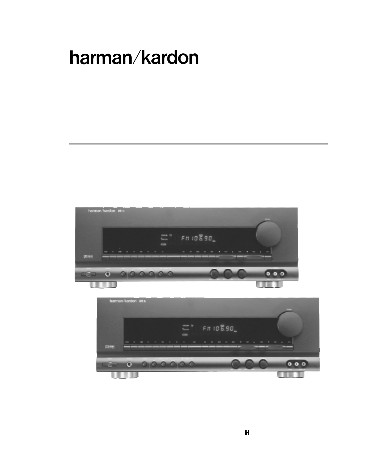
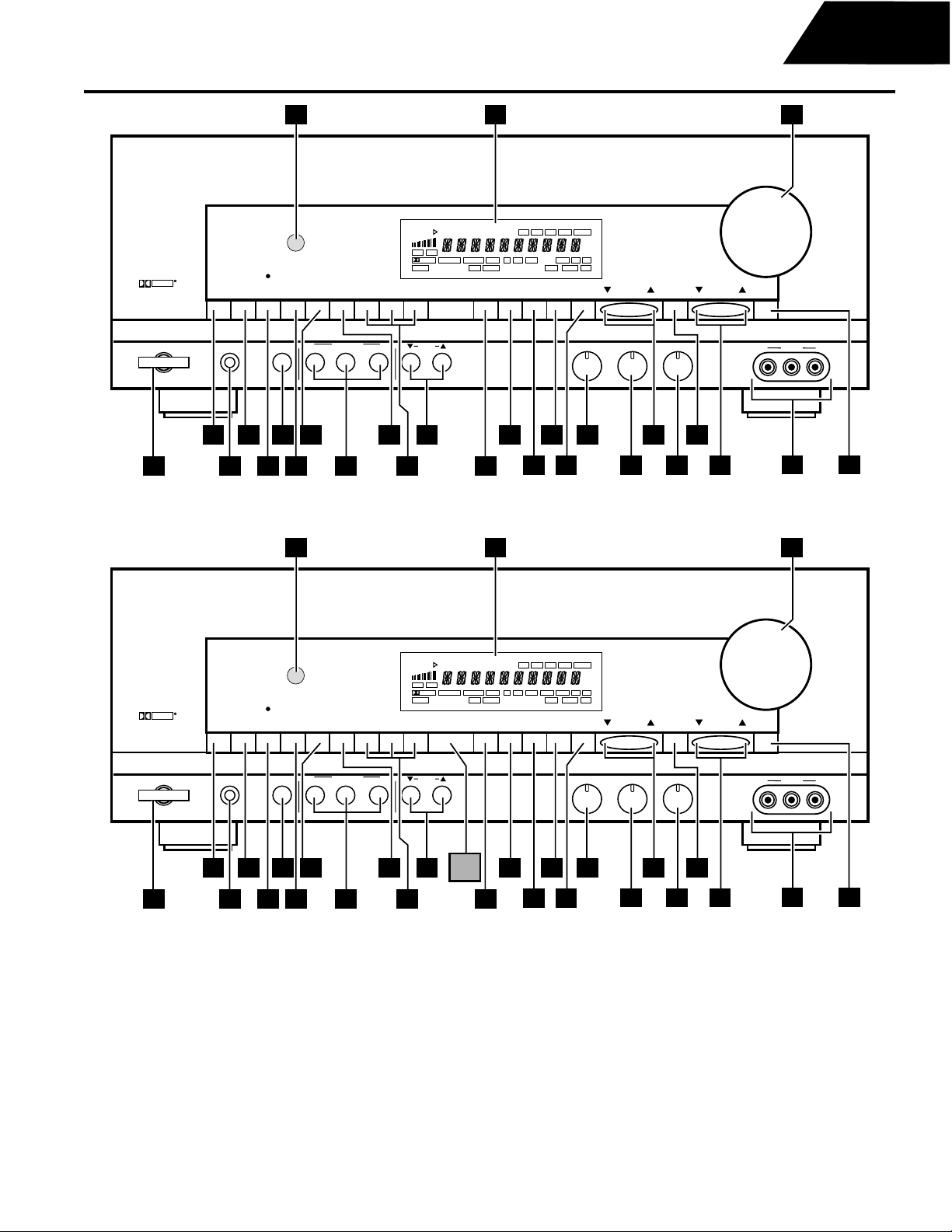
AVR75 & AVR85 FRONT PANEL CONTROLS
28 27 26
AVR75/85
harman/kardon
DOLBY
DIGITAL
Power
AM/FMCDCD
Phones
AVR 75
T-1/MON
Night
T-2TVTV
RF
DVDV1V1V2V2
Digital Input
Coax
OPT
VISUAL
TV DVD V1 V2
AC-3 PCM
DIGITAL PRO LOGIC 3 STEREO
STEREO
Mode
HALL
MOVIE RF OPT
MATRIX
OSD
TEST
V3
ATT
COAX NIGHT LFE ATT
MEMO
2 4 6 8 10 12 14 16 18 20 22
135791113
15 17
28 27 26
harman/kardon
AVR 85
MEMO
AUTO
SLEEP P-SCAN DISP
Volume
TUNED
STEREO
dB
kHz
MHz
CLR
MODE
P-SET
P-SCN
Treble
Bass
Min
Min
Max
L
Max
19 21 23
Balance
TUNE
MUTE
VIDEO 3
R
Video
L - Audio - R
24 25
Volume
VISUAL
TV DVD V1 V2
AC-3 PCM
DIGITAL PRO LOGIC 3 STEREO
STEREO
DOLBY
DIGITAL
Power
AM/FM
2 4 6 8 10 12 14 16 18 20 22
Phones
T-1/MON
T-2
Night
DVD
Digital Input
OPT
RF
Coax
V3 MULTIV3OSD
Mode
2929
135791113
1. Power: Press this button once to turn the unit on and off.
Once the unit is turned on, it may be turned off and then on
again from the remote, if desired.
NOTE: When the remote is used to turn the unit off the LED
surrounding the Power Switch will turn amber, indicating
that the AVR75/85 is in a Standby mode. In this condition
the unit is NOT disconnected from the AC main power
supply.
TEST
MEMO
AUTO
TUNED
STEREO
SLEEP P-SCAN DISP
CLR
MODE
Min
dB
kHz
MHz
P-SET
Treble
Bass
Min
Max
19 21 23
P-SCN
L
Max
Balance
TUNE
MUTE
VIDEO 3
R
Video
L - Audio - R
24 25
HALL
V3
MOVIE RF OPT
MATRIX
COAX NIGHTMULTI LFE ATT
ATT
MEMO
15 17
2. AM/FM Tuner Selector: Press this button once to select
the tuner. Press it again to switch between AM and FM.
3. Headphone Jack: Plug standard stereo headphones into
this jack for private listening.
NOTE: When the headphones are in use the output to the
speakers is muted and the surround mode is automatically
switched to
STEREO. When the headphones are removed
from the jack, sound to the speakers is restored and the unit
returns to the previous sound mode.
5
Page 6

Harman Kardon
Dolby Digital Audio/Video Receiver
AVR75/85
4. CD: Press this button to select the CD player.
5. Tape 1/Monitor: Press this button to select Tape One as
the input source. A red LED above the button will illuminate
to indicate that the Tape Monitor has been selected.
6. Night Mode: Press this button to activate the “Night”
mode, preventing loud playback when the digital modes are
in use.
7. Tape 2: Press this button to select tape 2 input.
8. TV Input: Press this button to select the source
connected to the TV Input (38).
9. Digital input Selectors: Press one of these buttons to
select a digital input source. The digital audio source may
be the same as, or different from, the analog audio of the
selected video source.
10. DVD Input: Press this button to select the source
connected to the DVD Input (37). Note that the DVD or LV
player’s digital audio output is used, it must be selected
separately using the Digital Input Selectors (9).
11. Video Sources: Press any of these buttons to select a
video input source.
20. P-Set: Press this button to manually scroll up or down
through the FM or AM stations programmed into the
receiver’s preset memory.
21. Balance: This knob adjusts the balance between the
front left and right speakers.
22. P-Scan: Press this button to automatically scan through
the FM or AM stations preset into the receiver’s memory.
Press the button again to stop the scan when the tuner is at
the desired station.
23. Tune: Press this button to manually scan up or down
through the FM or AM bands.
24. Video 3 Input: Audio or Video sources connected to
these jacks may be selected by pressing the Video Source
button (11).
25. Mute: Press this button to cut the output to the
speakers. Press it again to return to the previous volume
level.
26. Volume Control: Turn the knob clockwise to increase
volume, counterclockwise to decrease the volume. Note
that approximately two revolutions of the knob are required
to go from no output to maximum volume.
12. Mode: Press these buttons to scroll up or down through
the list of available surround modes.
13. OSD (On-Screen Display): Press this button to activate
the Attenuation mode which cuts the analog input signal by
50% to compensate for high-level input sources.
14. ATT Attenuation Mode Select: Press this button to
activate the Attenuation Mode which cuts the analog input
signal by 50% to compensate for high-level input sources.
15. Memo: The memo button is used to enter stations to the
tuner’s preset memory in either the manual or automatic
modes.
16. Clear: The clear button is used to cancel tuning,
memory input or when cleaning the unit’s memories.
17. FM Mode: Press this button to select the tuning mode
for FM stations.
18. Bass: This knob adjusts the tone of low-frequency
sounds. Turn it to the right to boost bass frequencies or to
the left to cut bass frequencies.
19. Treble: This knob adjusts the tone of high-frequency
sounds. Turn it to the right to boost high frequencies or to
the left to cut high frequencies.
27. Information Display: This display delivers messages
and status indications to help you operate the receiver.
Refer to the separate diagram for complete explanation of
the FL display.
28. Remote Sensor Window: The sensor behind this
window receives infrared signals from the remote control.
Aim the remote at this area and do not block or cover it
unless an external remote sensor is installed.
29. Multiroom Control: NOTE: this feature differentiates
the AVR85 from the AVR75. The AVR75 does not have
this feature. Press this button to turn the remote room feed
On or Off. The MULTI indicator (D) will light or flash when
the remote feed is On. Note that the remote feed will remain
On after the main room power is turned Off until it is
switched Off by pressing this button again.
6
Page 7

Harman Kardon
Dolby Digital Audio/Video Receiver
AVR75 & AVR85 FRONT PANEL DISPLAY
AVR75/85
AVR75 DISPLAY
S
A
S
VISUAL
AC-3
STEREO
PCM
DIGITAL
R
PRO LOGIC
R
Q
DVDV1V1V2V2
3 STEREO
HALL
MOVIERFRF
MATRIX
B
AVR85 DISPLAY
Q
V3
OPT
TEST
C
MEMO
COAX
AUTO
SLEEP
E
PPOONNM
M
TUNED
NIGHT
STEREO
LFE
P-SCAN
FGGHH
L
kHz
MHz
DISP
L
dB
ATT
K
J
I
VISUAL
AC-3
STEREO
PCM
DIGITAL
A
AC-3 Indicator: This indicator illuminates when the
A.
AVR75 is decoding a Dolby Digital input source.
Surround Mode Status: These indicators display the
B.
currently selected surround mode.
Digital Mode Indicators: These indicators show which
C.
digital input is in use.
Multi: This indicator signifies that the AVR85 is sending
D.
a program source to a remote room location. Note that it
may be illuminated even when the unit is “off” in the main
listening room, signifying that operation continues at
TVTVDVD
PRO LOGIC
B
3 STEREO
HALL
MOVIE
MATRIX
MEMO
OPT
TEST
COAX
V3
C
another location. When a remote command is being
received via the Multi IR connection (59), this indicator will
flash. NOTE: this feature differentiates the AVR85 from
the AVR75. The AVR75 does not have this feature.
Sleep Indicator: This indicator lights when the
E.
AVR75/85 is in the Sleep mode.
Night Indicator: This indicator lights when the
F.
AVR75/85 is in Night mode, which prevents the AVR75/85
from loud playback when digital sources are in use.
AUTO
TUNED
SLEEP
E
NIGHT
P-SCAN
MULTI LFE
DF
STEREO
dB
kHz
MHz
ATT
DISP
I
K
J
7
Page 8

Harman Kardon
Dolby Digital Audio/Video Receiver
AVR75/85
P-Scan: This indicator flashes when the stations
G.
programmed into the tuner memory are being automatically
reviewed.
LFE Indicator: This indicator will illuminate when the
H.
Low-Frequency Effects (LFE) option has been turned on
through the controls in
DISP: This indicator lights when the FL display has been
I.
turned off using the Display button (16) to remind you that
the unit is still turned on.
ATT Indicator: This indicator lights when the Attenuation
J.
function has been engaged to cut the input from analog
sources by approximately 50%.
Main Information Display: This ten-digit display shows
K.
messages relating to the status, input source, surround
mode, tuner, volume level or other aspects of unit’s
operation.
Stereo: This indicator lights when an FM station is
L.
broadcasting in stereo.
Tuned: This indicator lights when an AM or FM station is
M.
properly tuned and locked.
SETUP MENU 3.
Auto: This indicator signifies that the Automatic Tuning
N.
mode is in use for FM broadcasts.
Memo: This indicator flashes when the Memo button is
O.
pressed when entering presets and other information into
the tuner’s memory.
Test: This indicator flashes when the output levels are
P.
being set using the built-in test signal generator.
“Visual” Indicator: These indicators display which input
Q.
source is being fed to the video monitor output.
PCM Indicator: This indicator illuminates to show that a
R.
standard PCM (S/P-DIF) digital audio signal is being
decoded by the digital-to-analog converter.
Signal Level Indication: This is a visual indication of the
S.
the strength of a radio station signal. The more bars visible,
the stronger the station.
8
Page 9
Harman Kardon
Dolby Digital Audio/Video Receiver
28 2827 27
AVR75/85
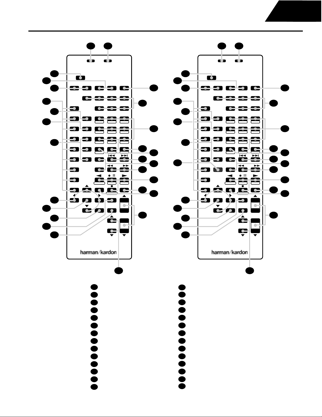
AVR75 & AVR85 REMOTE CONTROL
Sending Sending
11
22
Use Use
33
44
55
66
77
AM/FM AM/FM
TAPE 1 TAPE 1
TAPE 2 TAPE 2
Learn Learn
ON ONOFF OFF
Main Power Main Power
TV TV
DVD DVD
VID 1 VID 1
VID 2 VID 2
VID 3 VID 3
CD CD
ON ONOFF OFF
STEREO STEREOMATRIX MATRIXHALL HALL
NIGHT NIGHT
ABC ABC
DELAY DELAY
JKL JKL
RF RF
STU STUVWX VWXYZ YZ
OPT OPT
MEMO MEMO
COAX COAX
PRESET PRESET
DISC DISC
FM MODE FM MODE
DISPLAY DISPLAY
SELECT SELECT
Learning Learning
SLEEP SLEEP
Source Power Source Power
P/L P/L3ST 3ST
MOVIE MOVIEAC-3 AC-3
26 26
25 25
1 12 23 3
DEF DEFGHI GHI
4 4
7 78 89 9
**
++
__
RDS DISP. RDS DISP.
TEST TONE TESTTONE
6 6
5 5
MNO MNOPQR PQR
# #
0 0
CLEAR CLEARP-SCAN P-SCAN
SKIP SKIP
TUNE/ TUNE/
TUNE/ TUNE/
SEARCH SEARCH
SEARCH SEARCH
24 24
23 23
22 22
21 21
20 20
8
MULTI
19 19
/ /
PTY PTY
AF AF
MUTE MUTE
18 18
17 17
16 16
99
CH SELECT CH SELECT
OSD OSD
10 10
11 11
12 12
OSD OSD
VOLUME VOLUME
SPEAKER SPEAKER
15 15
13 13
AVR 75 AVR 85
14 14
Use/Learn
1
Source Power
2
Main Power
3
Source Selection
4
Night Mode
5
Delay
6
DigitalAudio Input Selectors
7
Multiroom Control
8
Menu Controls
9
Select
10
OSD
11
Test Ton e
12
Channel Select
13
Speaker LevelAdjust
14
Main Volume
15
Display
16
Mute
17
Transport Controls
18
Tune/Search and Fast Forward
19
Preset/Disc
20
Channel/Skip
21
Memo
22
P-Scan
23
Number Keys
24
Surround Mode Selection
25
Sleep
26
Learn LED
27
28
Sending LED
9
Page 10

Harman Kardon
Dolby Digital Audio/Video Receiver
AVR75 & AVR85 REMOTE CONTROL INFORMATION ...continued
AVR75/85
Use/Learn: This switch selects the operation mode of the
1.
remote control. Slide it to the left for normal operation. Slide
it to the right when the remote is being programmed.
Source Power: When power on/off commands have
2.
been programmed into the remote’s memory, press these
buttons to control power for the last source device selected.
Main Power: Press these buttons to turn the unit on or
3.
off (to Standby Mode).
Source Selection: Pressing one of these buttons selects
4.
the input source that will be listened to through the receiver.
When a source is selected the remote’s transport and
numeric number buttons will also transmit the commands
needed to control that machine.
Night Mode: Press this button to activate the “Night”
5.
mode, preventing loud playback when the digital modes are
in use without altering the dynamic range of the output
signal.
Delay: Press this button to change the delay for the
6.
surround channels when the Surround Mode Menu is on the
screen.
Digital Audio Input Selectors: Press one of these
7.
buttons to select a digital input source. The digital audio
source may be the same as, or different analog audio of the
selected video source.
Multiroom Control: Press this button to turn the remote
8.
room feed on or off. The Multi indicator will light or flash
when the remote feed is on. Note that the remote zone feed
will remain on after the main room power is turned off until it
is switched off by pressing this button again.
Menu Controls: These buttons control the action of the
9.
cursor or the selection of menu items when the receiver is
being configured using the setup menus.
D
Test Tone: Press this button to begin calibration of the
12.
output level for each channel. A test signal will immediately
be heard from the left front speaker and the Test indicator
P
will flash.
Channel Select: Press this button to view a status
13.
report of the output level for each channel. When the Test
Tone is audible and the system output levels are being set,
pressing this button will advance the channel being adjusted
in a clockwise direction to the next channel.
Speaker Level Adjust: When setting the system output
14.
levels, press these buttons to increase or decrease the
output level.
Main Volume: These buttons control the unit’s volume.
15.
Note that all channels are controlled simultaneously.
Display: Press this button to turn off all displays and
16.
indicators in the Information Display except for a small Disp
indication in the lower right corner of the display . Press
the button again to turn the display back on.
Mute: Press this button to temporarily cut the audio
17.
output of the receiver. Press it again to return to the
previous volume level.
Transport Controls: These buttons may be
18.
programmed to control the tape or disc motion of the last
playback source selected with the Source Selection
buttons . Use them as you would the Play, Stop, Pause,
Record, Reverse Play and Forward Play buttons on any
VCR, CD, cassette, DVD or LD remote control. The
Reverse Play button also operates the FM Mode
function of the AVR75/85’s tuner.
4
I
NOTE: The , and buttons are also used
to control the PTY, AF and RDS Display functions of the
tuner.
Select: This button enters settings to the receiver’s
10.
memory during system configuration.
OSD: Press this button to activate the on-screen menu
11.
system.
Tune/Search & Fast Forward: These buttons may be
19.
programmed to have multiple functions, which vary
according to the input device selected.
a. When the TUNER has been selected, these buttons
are used to tune stations.
b. When CD, Tape, DVD, LD or VCR is the input source,
these buttons act as the Fast Scan Forward or
Fast Scan Reverse controls.
10
Page 11
Harman Kardon
Dolby Digital Audio/Video Receiver
Preset/Disc: These buttons have multiple functions,
20.
which may vary according to the input device codes
programmed.
a. When the TUNER has been selected, these buttons
will scroll up or down through the stations
that have been programmed in the preset memory.
b. When CD is selected and the unit is a CD changer,
these buttons will change to the next disc or
previous disc .
c. When Tape 1 or Tape 2 is the input source, and the
tape machine is a compatible Harman Kardon dual
cassette deck, these buttons will switch between the
“A” and “B” sides.
Channel/Skip: These buttons have multiple functions,
21.
which vary according to the input device selected and the
codes programmed from another remote.
a. When TV, Vid 1 or Vid 2 are selected, they may
function as the channel up or channel down
tuning buttons when programmed with the codes from
another unit’s remote.
b. When CD is selected these buttons act as forward and
reverse “Skip” buttons to move to the next track or
chapter on the disc.
c. When a compatible Harman Kardon cassette player
has been selected as Tape 1 or Tape 2, these
buttons move the tape forward or backwards
to the next selection using the Music Scan feature.
Memo: The memo button is used to enter stations to
22.
the tuner’s preset memory in either the manual or automatic
modes. It is also used in the process of clearing the
memory. This button also performs the functions of the “ ”
symbol on compatible equipment.
P-Scan: Press this button to automatically scan through
23.
the stations preset into the tuner memory. Press the button
again to end the scan when the tuner stops at the desired
station. This button also performs the functions of the “ ”
symbol on compatible equipment.
AVR75/85
NOTE: The 0 button has a dual function. It also serves
as the CLEAR button for use in programming the tuner
or clearing the system memory.
Surround Mode Selection: Press one of these buttons
25.
to select a surround mode for the current listening session.
Sleep (AVR75): Press this button when the Sleep timer
26.
has previously been activated to view the time remaining
before the unit turns off to the Standby Mode. To activate
the Sleep function, first put the unit in the Tuner Mode by
2
min
4
E
OFF
4
E
O
22
15
26
30
min
60
min
90
OFF
pressing the AM/FM button . Next, press the Sleep
button and note that the Sleep and Memo indicators
button and then press the Sleep button again to set
26
O
will blink. Within that blinking time press the Memo
22
15
the sleep time in the following order:
10
min20min30min40min50min60min90min
When the desired time is shown in the display, press the
22
Memo button to enter the time. The unit will go into
15
the Standby Mode when the time entered has elapsed.
Sleep (AVR85): Pressing this button when the Sleep
26.
timer has previously been activated allows you to view the
time remaining before the timer function turns the unit off.
When the remote is in the AM/FM mode , the Sleep
function may also be changed or set by pressing this button
so that the Sleep and Memo indicators blink (timer not
yet set) or Sleep time is indicated (timer set already). Within
that time press the Memo button so that both
indicators blink slowly. Now press the Sleep button
again to set the desired sleep time in the following order:
min
10
min
20
When the desired time is shown in the display, press the
22
Memo button to enter the time. The unit will go into
15
the Standby Mode when the time entered has elapsed.
Learn LED: This indicator will illuminate when a button
27.
on the remote is being programmed with signals from
another remote during the “learning” mode. The light will go
out when the signal is received and memorized.
Number Keys: These buttons serve as a ten button
24.
numeric keypad to enter tuner preset positions. They are
also to be used to select channel numbers when TV has
been selected on the remote, or to select track numbers on
a CD, DVD or LD player, depending on how the remote has
been programmed. The letters below the buttons are used
to enter information for tuner station names.
Sending LED: This indicator should flash any time a
28.
button is pressed to confirm that a command is being sent to
the receiver or another unit. If the light is dim or does not
illuminate when a button is pressed the batteries in the
remote should be replaced.
11
Page 12
Harman Kardon
Dolby Digital Audio/Video Receiver
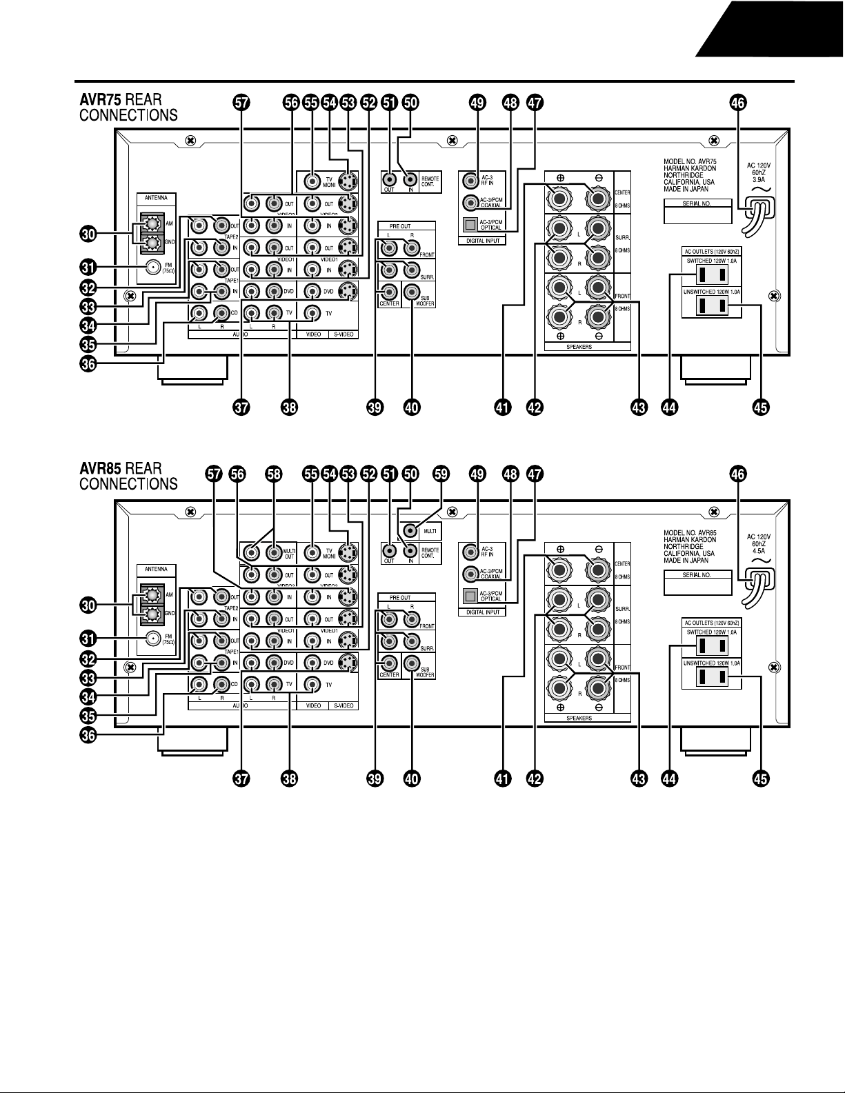
AVR75 & AVR85 REAR PANEL CONNECTIONS
AVR75/85
30. AM Antenna: Connect the AM loop antenna supplied
with the receiver to these terminals. If an external AM
antenna is used, make connections to the AM and GND
terminals in accordance with the instructions supplied with
the antenna.
31. FM Antenna: Connect an indoor or external FM
antenna to this terminal.
32. Tape 2 Out: Connect these jacks to the
RECORD/INPUT jacks of a second audio recorder.
33. Tape 2 In: Connect these jacks to the PLAY/OUT jacks
of a second audio recorder.
34. Tape 1 Out: Connect these jacks to the
RECORD/INPUT jacks of an audio recorder.
35. Tape 1 In: Connect these jacks to the PLAY/OUT jacks
of an audio recorder.
36. CD IN: Connect these jacks to the output of a compact
disk player or CD changer.
12
Page 13

Harman Kardon
Dolby Digital Audio/Video Receiver
AVR75/85
37. DVD Inputs: Connect the analog audio outputs and
composite or S-Video output of a DVD or LV player to these
jacks.
38. TV Inputs: Connect these jacks to the audio and video
outputs of a TV Tuner, Cable TV converter box, satellite
receiver, or any other audio/video source.
39. Pre-Outs: If external power amplifiers are used for any
channels, connect them to these jacks.
40. Subwoofer Pre-Out: Connect this jack to the line level
input of a powered subwoofer. If an external subwoofer
amplifier is used, connect this jack to the subwoofer
amplifier input.
41. Center: Connect these terminals to the center speaker.
42. Surround: Connect these terminals to the surround
speakers.
43. Front: Connect these terminals to the front speakers.
44. Switched AC Outlet: This outlet may be used to power
any device that you any wish to have on when the unit is
turned on.
45. Unswitched AC Outlet: This outlet, may be used to
power any AC device. The power will remain on at this
outlet regardless of whether the AVR75/85 is on or off.
NOTE: The power consumption of the device plugged into
each of these outlets should not exceed 120 watts.
46. Power Cable: Connect the AC plug to a non-switched
AC wall output.
47. AC-3/PCM Optical Input: Connect the optical digital
output from a DVD player, HDTV receiver, LV player or CD
player to this jack. The signal may be either a Dolby Digital
(AC-3) signal or a standard PCM digital source.
48. AC-3/PCM Coaxial Input: Connect the coax digital
output from a DVD player, HDTV receiver, LV player or CD
player to this jack. The signal may be either a Dolby Digital
(AC-3) signal or a standard PCM digital source.
50. Remote IR In: If the AVR75/85’s front panel IR sensor is
blocked due to cabinet doors or other obstructions, an
external IR sensor may be used. Connect the output of the
sensor to this jack.
51. Remote IR Out: This connection permits the IR sensor
in the receiver to serve other remote controlled devices.
Connect this jack to the “IR IN” jack on Harman Kardon or
other compatible equipment.
52. VCR 1 Inputs: Connect these jacks to the audio, video
and S-Video PLAY/OUT jacks of a VCR.
53. VCR 1 Outputs: Connect these jacks to the audio,
video and S-Video RECORD/IN jacks of a VCR.
54. TV Monitor S-Video Output: Connect this jack to the
S-Video input of the TV monitor or video projector to view
S-Video sources selected by the receiver’s video switcher.
NOTE: Standard (composite) video and S-Video signals will
appear only at their respective output. The AVR75/85 does
not convert one video format to anther.
55. TV Monitor Video Output: Connect this jack to the
standard (composite) video input of a TV monitor or video
projector to view the on-screen menus and the output of any
standard video source selected by the receiver’s video
switch.
56. VCR 2 Outputs: Connect these jacks to the audio,
video and S-Video RECORD/IN jacks of a second VCR.
57. VCR 2 Inputs: Connect these jacks to the audio, video
and S-Video PLAY/OUT jacks of a second VCR.
58. Multiroom Audio Outputs: Connect these jacks to the
optional audio power amplifier that powers remote room
speakers with the input selected by the multiroom control
system. This feature is found only on the AVR85.
59. Multi IR: Connect the output of an IR sensor in a remote
room to this jack to operate the AVR85’s multiroom control
system. This feature is found only on the AVR85.
49. AC-3 RF Input: Connect the AC-3 RF output of an LV
player equipped for digital audio to this jack.
NOTE: Do not connect standard analog sources to these
jacks (48)(49).
13
Page 14

Harman Kardon
Dolby Digital Audio/Video Receiver
AVR75/85
Service Bulletin #9705 for AVR85
Service bulletin # 9705 August 1997
To: All harman/kardon Service Centers
Models: AVR85
Subject: No audio output
In the event you receive an AVR85 with the complaint “no audio output” (even though the display is
lit up normally), perform the necessary steps listed below:
PROCEDURE:
1) Make sure the receiver is OFF and unplugged; remove the top cover of the unit.
2) Position the unit on its side, facing it so you are looking at the bottom cover, with the front of the receiver
facing left. The power transformer should be down, or nearest the work bench.
3) Remove the front right “foot” of the unit; then with a sharp pair of dikes or wire cutters cut the (16) metal
connections on the bottom screen attaching it to the bottom cover. Remove bottom screen from unit; for
safety continue to cut all the remaining severed metal tabs from the bottom cover.
4) Locate and discharge main power supply electrolytic capacitors C802 & C803 with a 10 ohm, 10 watt resistor.
At this point, C802 & 803 are at the top of the main PCB; The two leads to C803 can be identified by the
marking “-B” on the PCB; C802 is just above it. After discharge, check with voltmeter that capacitors have
less than 1 volt DC across leads to confirm that discharge is complete.
5) See drawing; locate two areas of a poor solder connection due to an unintended mask, or dark-colored dot
that is partially covering the solder pad(s) where the leads come through. Unsolder the connection(s) with
solder wick. Clean & scrape, if necessary, with a small screwdriver the foil/pad area thoroughly and remove
any excess mask residue. Re-solder the connection(s) carefully to assure good connections.
6) Turn the unit upright; locate PCB P714, the small vertical circuit board nearest the main heatsink. Unplug
and remove small molex connector J701 at the top of the board; then remove the four mounting screws and
metal tabs holding the top of the board in place.
7) Remove the two locks to the two sockets, J714 and J716. Take care not to damage the lock or connector
while attempting to unlatch the PCB; then unplug and remove the entire PCB P714.
8) Locate 10 ohm, ¼ watt resistors RH23, RH24, R745, R746, R747, R748; test with multimeter to assure they
are still 10 ohms +/- 5%. If values are different (indicating damage), replace as necessary.
9) Return PCB P714 to unit; re-attach molex connector; replace 4 screws and mounting tabs. Replace top cover
of receiver.
10) Re-attach the bottom screen to the bottom cover using 12 screws, (H/K# 51260306MO); the screen will be
upside-down compared to its former position when attached; replace the unit’s “foot”.
11) TO TEST:
a) Plug in the unit; connect speakers to left, right, and center output terminals.
b) Turn the unit on; switch the unit to “Prologic” mode by use of the mode buttons on the front panel.
c) Press the button “TEST TONE” on the remote control. The display should read “FRONT L” and “TEST”
should flash.
d) Adjust the master volume, and verify test noise is heard from front left channel.
e) Press the button “CH SELECT” on the remote control to change to the right and center speakers, and
verify test noise is heard from each one.
f) Press the button “TEST TONE” on the remote control again to exit the test.
Model
AVR85
AVR85
Serial number
120V
MJ0011-01001
to
MJ0011-02500
MJ0011-02501 and
above
Serial number
230V
MJ0012-01001
to
MJ0012-01500
MJ0011-01501 and
above
Status Action
Poor connections in
two areas on main
PCB
Modified by factory NONE REQUIRED
Clean & re-solder connections, check
or replace RH23,RH24,R745.R746,
R747, R748 if necessary
14
Page 15

Harman Kardon
Dolby Digital Audio/Video Receiver
View is upper left-hand corner of PCB
Bottom (trace) side
AVR75/85
CONNECTION #1
CONNECTION #2
15
Page 16

Harman Kardon
Dolby Digital Audio/Video Receiver
AVR75/85
SERVICE AND ADJUSTMENT
I. SERVICE PROCEDURE
1.Tracking Point Memory
This service procedure can be used for measurement of the tuner circuit. With the POWER ON, press the “PRESET UP”
button while pressing the “MEMO” button for at least 3 seconds or more. FLD will display “TRACKING”. Frequencies to be
memorized are as follows:
VERSION P1 P2 P3 P4
FM
AM
US, Europe. 90.0 98.0 106.0 87.5
SCAN STEP P5 P6 P7 P8 P9 P10 P11 P12~P30
10 KHz 600.0 1000.0 1400.0 520.0
9 KHz 603.0 999.0 1404.0 531.0
MW/LW 171.0 207.0 270.0 152.0 531.0
2. FLD Segment Illumination
This service procedure will illuminate all segments by the following step: With the POWER ON, press the “FM/AM (TUNER)”
button while pressing the “MODE” button for at least 3 seconds or more. This procedure takes 1 minute and 40 seconds to
finish; at this point the procedure is complete.
Sequence
1. All segments will be illuminated for 5 seconds.
2. At the grid “1G”, segments are illuminated in the following order:
3. At the grid “2G” to “11G”, each segment is illuminated individually:
4. At the grid “12G”, segments are illuminated in the following order:
16
Page 17
Harman Kardon
Dolby Digital Audio/Video Receiver
AVR75/85
3. All Clear
This service program can clear all memorized operations and functions. With the POWER ON, press the “CD” button while
pressing the “MODEs” button for more than 3 seconds. FLD shows “CLEAR MEMO” and power will be OFF.
II. ELECTRICAL ADJUSTMENT
1. Main amp idling current adjustment.
1) With the power OFF, set variable resistor R755 (Lch), R756 (Rch) RH28 (Center ch) on the PC board (P704)tothe
center position.
2) Locate test points J723 (Lchan) J724 (Rchan) and J725 (Centerchan). These are 3 pin female molex connectors on the
MAIN PCB. Attach a DC voltmeter (set to a low range) to the two outer pins on each test point. This is best accomplished
by making up a “test plug” using a male molex connector that fits into the one in the unit, with wires attached, for
connection to the voltmeter. An alternate method is to use two “mini-grabbers” to attach to the two outer pins on each
connection. The middle pin has no connection.
3) After the above, adjust the idling current as follows: Turn the power ON and adjust variable resistor R755 (Lch), R756
(Rch), RH28 (Center ch) while observing the reading on the voltmeter.
*The target value is 11mV (25 mA).
NOTE:
When a unit whose idling current has been adjusted is switched on after 1 minute it reaches about 4.7~5.5mV. After 30
minutes, it reaches a balanced state and stabilizes at 8.9-11mV (target). Therefore, if the adjustment is made 30 seconds
after the power is switched on, adjust to 3.5 ~ 4.0mV. In the same way, if 1 minute has passed since the power was
switched on, adjust to 4.7 ~ 5.5mV. From 1 to 2 minutes, adjust to 6.2 ~ 6.4mV. From 2 to 4 minutes, adjust to 7.1 ~
7.6mV. From 4 to 7 minutes, adjust to 7.9 ~ 9.0mV. After more than 7 minutes since the power was switched on, adjust to
the setting of 10.5 ~ 11.2mV. Here is a reference table for the adjustment values:
Time since power switched on Idling current adjustment
30 seconds 3.5 ~ 4.0mV
1 minute 4.7 ~ 5.5 mV
1 - 2 minutes 6.2 ~ 6.4mV
2 - 4 minutes 7.1 ~ 7.6mV
4 - 7 minutes 7.9 ~ 9.0mV
More than 7 minutes 10.5 ~ 11.2mV
III. ALIGNMENT PROCEDURES
Test Equipment Required
1) AM/FM Signal Generator
2) Video Signal Generator
3) Digital Multimeter
4) Distortion level meter
1. AM IF Adjustment
Step
1
Input Signal Source
Connection
Signal generator output to
transmission loop antenna.
(:Standard required loop)
Signal
Frequency
999 KHz
(Europe)
1000 KHz
(USA)
Source Signal Output Level
and Modulation
Level 300m V/m (50dB/m)
Mod. 400 Hz 30%
Reception
Frequency
Tuning point LA06
Adjustment
Point
REMARK: For receiving antenna, the one supplied with the unit is adequate.
This adjustment is not normally necessary, because the coil LA06 is preset by the original supplier.
Adjustment
Value
Output level
(L or R)
Maximum
at TAPE-OUT
17
Page 18
Harman Kardon
Dolby Digital Audio/Video Receiver
2. AM Tracking Adjustment
AVR75/85
Step
1
2
3
Input Signal Source
Connection
Signal generator output to
transmission loop antenna.
(:Standard required loop)
Repeat steps 1 and 2 until sensitivity is maximized.
3. AM Tracking Adjustment (LW)
Step
1
2
Input Signal Source
Connection
Signal generator output to
transmission loop antenna.
(:Standard required loop)
Signal
Frequency
603 kHz
(Europe)
600 kHz
(USA)
1404 kHz
(Europe)
1400 kHz
(USA)
Signal
Frequency
171 kHz
270 kHz
Source Signal Output
Level and Modulation
Level 300 - 400 m V/m
Mod. 400 Hz 30%
Level 300 - 400 m V/m
Mod. 400 Hz 30%
Source Signal Output
Level and Modulation
Level 300 - 400mV/m
Mod. 400 Hz 30%
Level 300 - 400mV/m
Mod. 400 Hz 30%
Reception
Frequency
603 kHz
(Europe)
600 kHz (USA)
1404 KHz
(Europe)
1400 KHz (USA)
Reception
Frequency
171 kHz LA03
270 kHz CA08
Adjustment
Point
LA01
CA01
Adjustment
Point
Adjustment
Value
Output level (L
or R)
Maximum at
TAPE-OUT
Output level (L
or R)
Maximum at
TAPE-OUT
Adjustment
Value
Output level
(L or R)
Maximum
at TAPE-OUT
Output level
(L or R)
Maximum
at TAPE-OUT
3
Repeat step 1 and 2 until sensitivity is maximized.
4. AM Auto Stop Adjustment
Step
1
2
Input Signal Source
Connection
Signal generator output to
transmission loop antenna.
(:Standard required loop)
REMARK: This adjustment is related to the FM muting Level Adjustment. The FM muting Level re-adjustment is necessary
after this adjustment.
Signal
Frequency
999 kHz
(Europe)
1000 kHz
(USA)
Source Signal Output
Level and Modulation
500 m V/m (54 dB/m)
1000 m V/m (60 dB/m)
Reception
Frequency
999 kHz
(Europe)
AUTO
SCAN
Adjustment
Point
RA11
Only Confirm
Adjustment
Valve
“TUNED”
indicate on FLD
“TUNED”
indicate on FLD
5. FM MONO. Distortion Adjustment
Step
1
Input Signal Source
Connection
Signal generator output to FM
antenna terminal. (75 W )
Signal
Frequency
98 MHz
Source Signal Output
Level and Modulation
500 m V (54 dB)
MONO 1 KHz/
Dev. 40 KHz 53.3%
(Europe)
MONO 1 KHz/
Dev. 75 KHz 100%
(USA)
Reception
Frequency
98 MHz
(P2)
Adjustment
Point
L201
Adjustment
Value
Distortion level
Minimum
at TAPE-OUT
18
Page 19
Harman Kardon
Dolby Digital Audio/Video Receiver
AVR75/85
6. FM Muting Level Adjustment
Turn the variable resistor R212 until the word TUNED is not shown in the display. Then adjust the resistor R212 in the
opposite direction until TUNED is shown in the display.
Step
1
2
Input Signal Source
Connection
Signal generator output to FM
antenna terminal. (75 W )
Signal
Frequency
98 MHz
Source Signal Output
Level and Modulation
6.3 m V (16 dB)
MONO 1 KHz/
Dev. 40 KHz 53.3%
(Europe)
MONO 1 KHz/
Dev. 75 KHz 100%
(USA)
Over mentioned level
+3 dB
Reception
Frequency
98 MHz
(P2)
AUTO
SCAN
Adjustment
Point
R212
Only Confirm
Adjustment
Value
“TUNED”
indicate on FLD
“TUNED”
indicate on FLD
7. FM STEREO Distortion Adjustment
Adjust the L channel with the RF signal modulated only L channel first and confirm the R channel with the RF signal
modulated only R channel.
Step
1
2
Input Signal Source
Connection
Signal generator
output to FM antenna
terminal. (75W )
Signal
Frequency
98 MHz
Source Signal Output
Level and Modulation
500 m V (54 dB)
L or R 1 kHz/
Dev. 40 kHz 53.3%
PILOT 19 kHz/
Dev. 6 kHz 8% (Europe)
L or R 1 kHz/
Dev. 67.5 kHz 90%
PILOT 19 kHz/
Dev. 6.75 kHz 9% (USA)
Reception
Frequency
98 MHz
(P2)
Adjustment Point
IF COIL
in
FRONT END
R218
Adjustment
Valve
Distortion level
Minimum
at TAPE-OUT
Distortion level
Minimum
at TAPE-OUT
REMARK: Adjustment with R218 is not necessary when the distortion level is less than 0.5% with adjusting IF coil.
8. FM STEREO Separation Adjustment
Step
1
2
Input Signal Source
Connection
Signal generator output to FM
antenna terminal. (75W )
Signal
Frequency
98 MHz
98 MHz
Source Signal Output
Level and Modulation
Same specification as
FM STEREO distortion
adjustment.
Input only L channel
Same specification as
FM STEREO distortion
adjustment.
Input only R channel
Reception
Frequency
98 MHz
(P2)
98 MHz
(P2)
Adjustment
Point
R211
R211
Adjustment
Value
Output level
Minimum
at TAPE-OUT
channel R
Output level
Similar as Rch
at TAPE-OUT
channel L
9. On Screen Display VCO Adjustment
Step
Input Signal Source and
Connection
Color bar or other standard
1
video signal.
Video signal generator
output to LD video input.
REMARK: Connect the TV monitor to the monitor output terminal of the product.
Measuring
Position
IC QX60
26pin and
GND
Measuring Equipment
DC voltmeter
(Impedance > 10k W /V)
Input
Selector
LD CX67 2.5V ± 0.1V
Adjustment
Point
Adjustment
Value
19
Page 20
Harman Kardon
Dolby Digital Audio/Video Receiver
AVR75/85
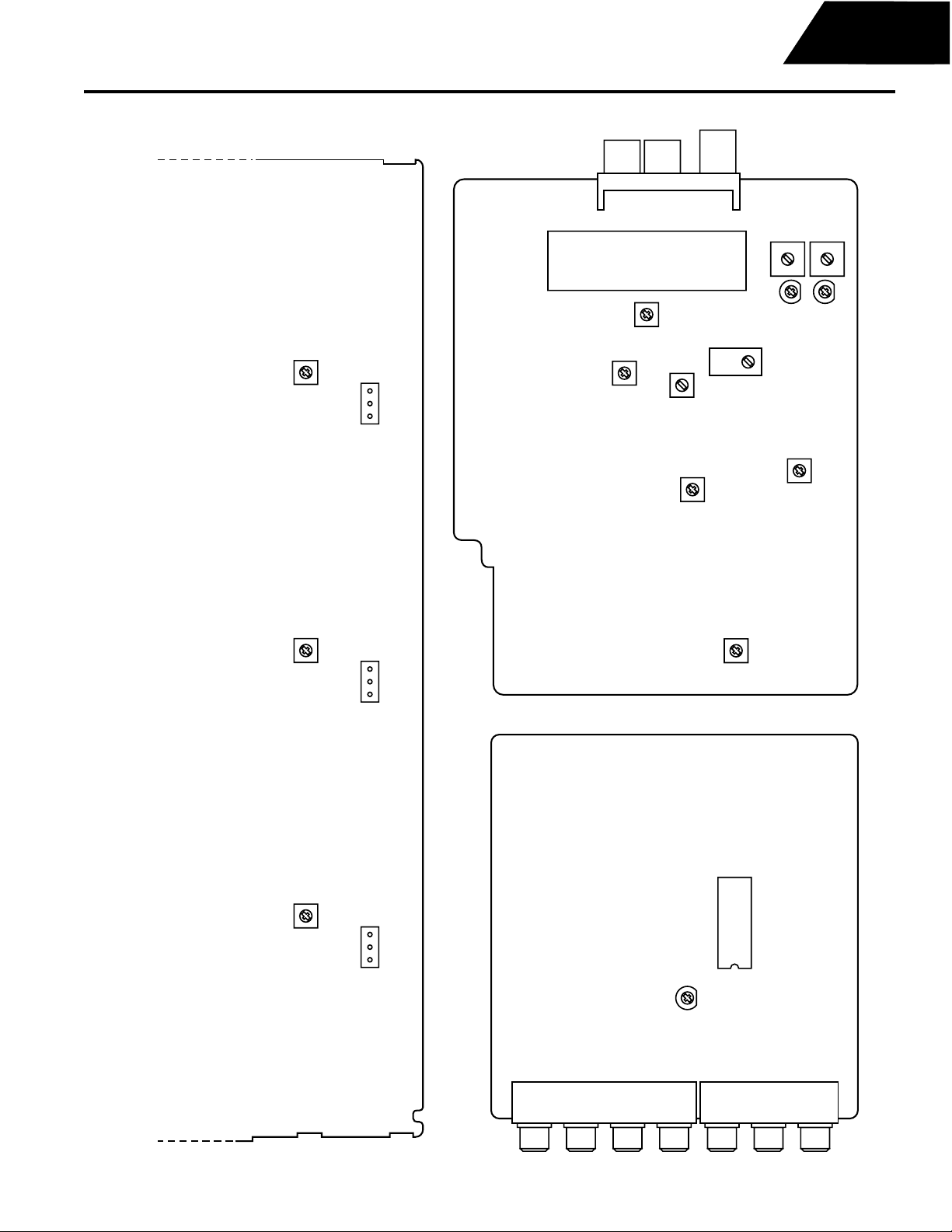
ALIGNMENT AND TEST POINTS
J101
LA01
R755
LEFT
R756
RIGHT
J723
J724
P104 - TUNER PCB
A101
LA03
CA08
R218
RA11
R201
R211
R906
LA06
CA01
R212
ALIGNMENT AND TEST POINTS
RH28
CENTER
J725
P704
MAIN PCB
PL04 - VIDEO SELECTOR PCB
CX67
16
30
OSD ADJ
15
QX60
1
20
Page 21

Harman Kardon
Dolby Digital Audio/Video Receiver
AVR75/85
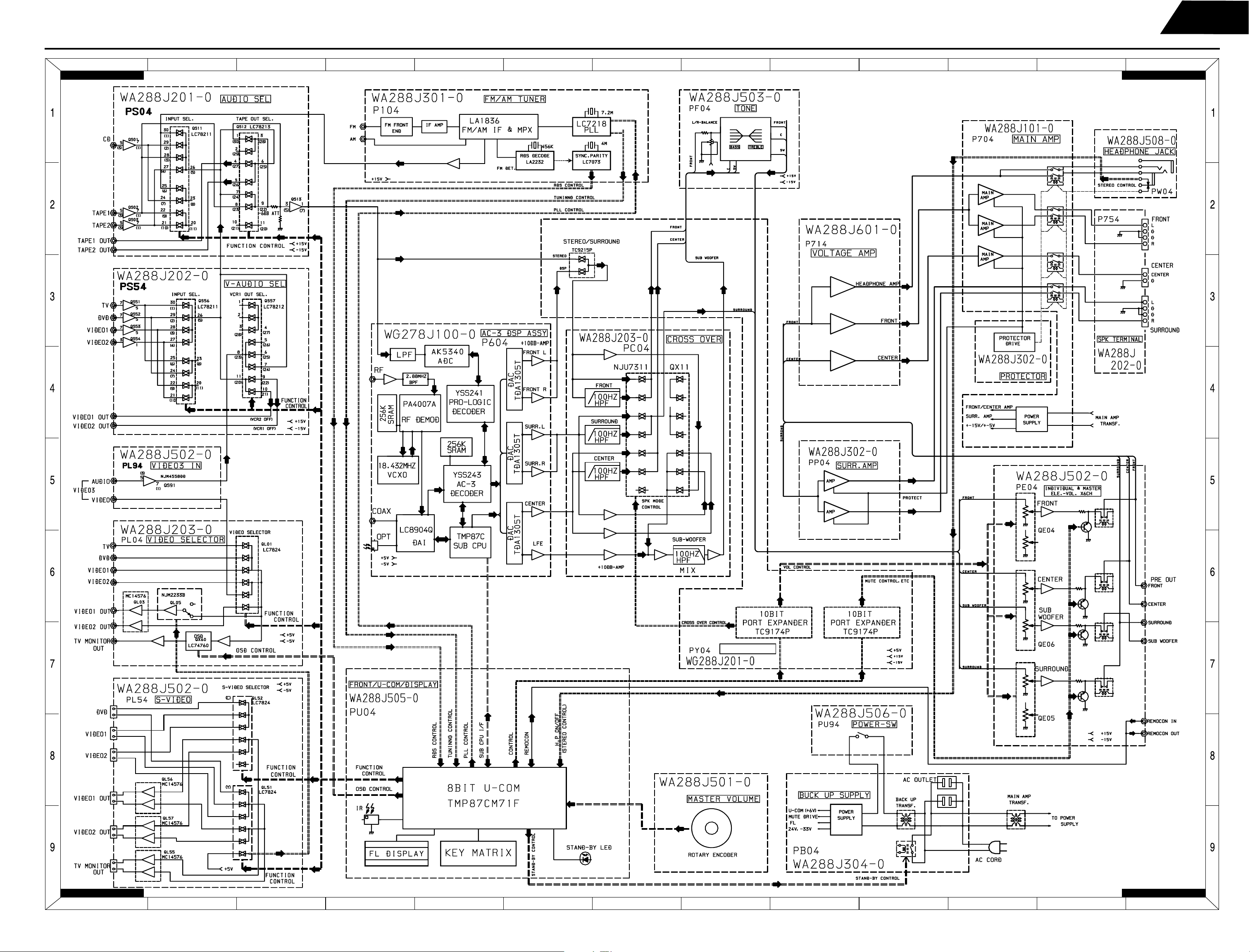
IV. TECHNICAL DESCRIPTION
This product is a “Dolby Digital (AC-3)” decoder. By connecting this product with a Dolby digital compatible component such
as a DVD player or DBS tuner, it will be capable of 5.1 CH (Front L/R, Rear L/R, Center and Sub-woofer) play.
This product is composed of approximately of 5 blocks including the AC-3 decoder & DAC block (P604), crossover block
(PC04), power supply block (P704), volume control block (PE04) and front key input block (PU04).
V. SIGNAL AND CIRCUIT DESCRIPTION
OPT/COAX (AC-3/PCM input)
This signal is based on an additional format for transmitting the AC-3 data through the conventional digital audio interface
(SPDIF). This SPDIF contains the compressed data for AC-3, instead of PCM Audio data. Similarly to the case of ROM data,
whether the data is audio or non-audio is identified according to the status in the signal. This signal can be output from a DVD
player, etc.
DAI (Digital Audio Interface) Receiver
This circuit extracts various clock and data signals from the signal input in the SPDIF format.
AC-3 Decoder DSP
This circuit generates the 6-channel data (Front L/R, Rear L/R, Center and LFE) based on the data output from the DAI, and
outputs the 6-channel data to the DAC as 3 sets of 2-channel data.
Crossover
This circuit consists of 100Hz HPF for each channel, 100Hz LPF for sub-woofer channel, and mixing for sub-woofer output.
Depending on the speaker mode setting, frequencies of this circuit will be changed.
21
Page 22
Harman Kardon
Dolby Digital Audio/Video Receiver
AVR75/85
AVR75/85 BLOCK DIAGRAM
AVR75/85 PAGE 22-1of4
EDCBA
HGF
I
J
LMK
AVR75/85 PAGE 22-2of4
PN54
PU54
CONNECT
AVR75/85
BLOCK DIAGRAM
AVR75/85 PAGE 22-3of4
AB CDE
FGH
AVR75/85 PAGE 22-4of4
J
K
LMI
22
Page 23
Harman Kardon
Dolby Digital Audio/Video Receiver
Power Suppies
USA/Canada ........AC120V, 60Hz
Europe ............AC230V, 50Hz
Dimensions (WxHxD)
Inches: ............17! x6* x 18"
mm ..............444x162x457mm
Weight (lbs/kgs) ........34/15.4
These specifications are service target specs. Specifications and components are subject to
change without notice. Overall performance will be maintained or improved.
General Test Conditions
AVR75/85
SPECIFICATIONS
1 Test Methods
2 Power Source
3 Tuner Measurements
4 Audio Measurements
5 Control Settings
Test methods for Tuners and Amplifier.
CP-2101, C6102, C6104
The amplifier shall be tested at the (Primary power supply) conditions shown
in table below.
Destination Power Source
U 120 Volts RMS ± 1% 60 Hz ± 2%
N 230 Volts RMS ± 1% 50 Hz ± 2%
The FM signal shall be 500uV (65dBf) with ± 75kHz
Deviation at 1000Hz and 50mV/m Loop injected with 30%
modulation at 400Hz for AM, unless otherwise specified.
TAPE OUT terminated with 47kohms load unless otherwise
specified.
All audio measurement shall be made with test signals injected into CD.
Inputs and output measured at SPEAKER outputs with 8ohms ± 1%
non-inductive resistor load, or at TAPE OUT with 10kohms ± 5%//1nF ± 5%
loads, unless otherwise specified.
Tone control : Mechanical center position
Balance control : Mechanical center position
Volume control : According to CP-2101
SPK SETT : ALL Large
ATT : off
unless otherwise specified
AC-3 Section Setting
Night Mode : off
SPK SETT NO. 1 Front: Small, Center: Small, Surround: Small, Subw: ON
SPK SETT NO. 2 Front: Large, Center: Large, Surround: Large, Subw: ON
SPK SETT NO. 3 Front: Large, Center: Large, Surround: Small, Subw: OFF
6 Used Test Disc Dolby AC-3 Demonstration & Test Laser Disc Ver. 1.0 (for AC-3 RF)
23
Page 24
Harman Kardon
Dolby Digital Audio/Video Receiver
Audio Section Performance Specifications
Seq # Test Reference Unit Nominal Limits
Continuous Power Output THD 0.09%
(L/C/R)
Front L/R both, Center Ch.
! FTC
! CP-2101 5 CD Input
5 Volume Max.
Continuous Power Output
Surround Ch. THD 0.7%
1
Both Channels Driven
! CP-2101 ! FTC
DIN 1% Power Output
Front Ch. 5 CD In
Dynamic Power Output
Front Ch.
! CP-2101
! CD IN
Power Bandwidth
THD 0.09% Front Ch.
2
! CP-2101 5 Volume: Max.
5 CD IN
Total Harmonics Distortion
at 65W Output Front Ch.
5 THD ! FTC
! CP-2101 ! Volume: Max.
Front L/R both, Center Ch.
5 CD IN MODE: STEREO
Surround L/R Ch.
3
Mode: PCM STEREO Service
SPK SETT NO. 2
Total Harmonics Distortion
at 0.25W Output Front Ch.
5 THD ! FTC
! CP-2101 ! Volume: Max.
5 CD IN MODE: STEREO
Intermodulation Distortion
at 65W Output
Front channel at STEREO Mode
5 CP-2101 (SMPTE Method)
4
5 Volume: Max.
Input Sensitivity for 1.0V Pre-Output
at CD IN Measured at 1kHz
Vol: Max, Mode: STEREO
Difference of Input Sensitivity
5
at each source ch., at CD IN 1KHz
Frequency Response at Output -3 dB
6
Mode: Stereo ref: 1KHz
Treble Action
(L, C, R)
7
Bass Action
(L, C, R, SW)
Crosstalk (between Stereo Channels)
terminated by 1k V
8
5 without Hum & Noise
5 CP-2101
8W 20Hz
8W 1kHz 80 ]65
8W 20kHz 80 ]65
8W üü
Surr.
Ch.
8W 1kHz 75 ]65
8W üü
8W 1kHz 85 ]75
8W 1kHz üü
4/2W 1kHz üü
8W 32.5W
W W
20Hz
FRONT Ch.
L/R/C
Surr. Ch.
10KHz
100Hz
(SW
40Hz)
Input: CD
STEREO
1kHz 0.01
20kHz 0.05
40Hz 0.5
1kHz 0.5
20kHz 0.5
20Hz 0.05
1kHz 0.05
20kHz 0.05
W
8W 0.03
W
Front L/R mV 240 200~280
Front L/R dB ü*1
Front L/R Hz 10~70k 15~50k
Boost
Cut 10
Boost 10
Cut 10
100Hz 59 ]50
1kHz 59 ]50
10kHz 59 ]50
W
Hz
%
dB
80 ]65
5~70k 10~60k
0.03
*0.09
*0.7
*0.09
*0.09
10
7.5~12.5
7.5~12.5
AVR75/85
24
Page 25
Harman Kardon
Dolby Digital Audio/Video Receiver
Seq # Test Reference Unit Nominal Limits
AVR75/85
10
11
12
13
Crosstalk (between Stereo Channels)
Measured at TAPE IN
9
terminated by 1kV
5 without Hum & Noise
5 CP-2101
Output Impedance
Referred to 1kHz
(SUB-WOOFER 40HZ)
Input CD
Input Impedance at 1KHz CD 47k ]40k
ATT Level at 1kHz
Minimum Volume Hum & Noise
Output, CD Input
Using 20kHz LPF
Input: CD
STEREO
STEREO Front
Surr. Mode
Pro Logic
(LARGE)
100Hz
1kHz 80 ]70
10kHz 80 ]70
Preout
Front
Preout
Center
Preout
Surround
Preout
Sub Woofer
Tape/Video1 1100 1000~1200
CD
Front 0.5 *1.0
Center 0.5 *1.0
Surround 0.5 *1.0
Sub
Woofer
PreOut
dB
W
dB 6 4~8
mV
80 ]70
550
0.5 *1.0
15 *20
350~
750
14
15
16
17
18
Front
Maximum Volume Hum & Noise
SPK Output, CD Input
Input shorted
Using: 20kHz LPF
A weighted (Except Subwoofer)
Signal to Noise Ratio
at 1kHz 1W Output
A weighted at short circuit
5 CP-2101
Signal to Noise Ratio at DOLBY
reference Level measured
CCIR/ARM weighted referred to1kHz
Input shorted
Measured at Preout terminal
PRO LOGIC/LARGE Master Vol.: 0dB
Dolby overload CD input Level at PREOUT terminal,
THD 1% (PRO LOGIC) Vol. 0dB
Damping Factor
at 32.5W (8V) Output
CD input, Front channel
Surround MODE:STEREO
Center LARGE 8.0 *15
Surround LARGE 8.0 *15
Sub
Woofer
STEREO
PRO LOGIC 8.0 *15
PRO LOGIC
DVD
0.5V Input
350mV Input
Front
350mV Input
Center
350mV Input
Surround
1kHz V 2 ]1.9
100Hz üü
1kHz 60 ]50
10kHz üü
mV
uV
dB
1.5 *3.0
150 *200
82 ]78
70 ]65
70 ]65
70 ]65
25
Page 26
Harman Kardon
Dolby Digital Audio/Video Receiver
AVR75/85
19
20
21
22 Power Consumption at STANDBY
DC offset of Speaker output
Volume Min.
No Load
Idling Power Consumption
at Minimum Volume Control
Power Consumption at Rated Power
L/R channel Driven
Front
Center
Surround ü*60
AC Line
AC Line 290 245~335
AC Line 7 *10
Video Section Performance Specifications for Model AVR75
Seq
#
1
2
Output Level for CVBS 1VP-p
(100%) White CVBS) Input
* at Monitor Output
* Output terminated by 75V
Output Level Difference
between each source
Output Level for Y/C
1Vp-p(Y), 0.28Vp-p(C) Input
* Measured S-Terminal
* at Monitor Output
* Output Terminated by 75V
Test Reference Units Nominal Limit
ü*60
mV
W
% +/-3%
ü*60
85 70~100
1.0
1.0
0.28
0.9~1.1
+/-5%
0.9~1.1
0.25~0.3
1
Output Level Difference
between each source
Input Impedance
3
4
5
* 1MHz, 1VP-p Sine Wave Input
* Output terminated by 75V
Output Impedance at 1Vp-p Output
* LD Input
* 1MHz, Sine Wave
Frequency Response at -3dB
Referred to 1MHz measured at
1Vp-p output
* Input LD
* Terminated by 75V
* Measured by Composite output
TV 75
Video1 75
Video2 75
Video3 75
Monitor 75
Video1 75
Video2 75
Monitor
Video1 8M ]6M
Video2 8M ]6M
%
V
Hz
+/-3%
+/-3%
75
8M ]6M
+/-5%
+/-5%
ü
ü
ü
ü
ü
ü
ü
ü
26
Page 27
Harman Kardon
Dolby Digital Audio/Video Receiver
FM Tuner Section Performance Specifications for Model AVR75/85
Seq # Test Measured Unit Nominal Limits
AVR75/85
1
2
3
Frequency Range
U Version
(MONO)
Usable Sensitivity at 75V
N Version
U, N,
Version
3 dB Limiting Sensitivity
U Version
50 dB
50K MHz
90MHz
98MHz
106MHz
90MHz
98MHz
106MHz
OTHERS
UV
(dBf)
98MHz
90MHz
98MHz
87.50~
108.00
1.3
13.5
1.3
13.5
1.3
13.5
1.3
13.5
1.3
13.5
1.3
13.5
2.6
19.5
0.8
9.3
1.9
16.8
1.9
16.8
ü
*2.5
*19.2
*2.5
*19.2
*2.5
*19.2
*3.0
*20.8
*3.0
*20.8
*3.0
*20.8
*6.0
*26.8
*1.3
*13.5
*3.3
*21.6
*3.3
*21.6
4
5
6 Muting Threshold
7 Muting Window width at 98MHz
8
9 Mono Distortion
10 Overload Brake up
MONO Quieting Sensitivity
MONO S/N Ratio at 98MHz
MONO Hum & Noise at 98MHz
Frequency Response
referred to 30Hz-15kHz
De-Emphasis
N Version
50 dB
106MHz
90MHz
98MHz
106MHz
500uV
(65dBf)
75uS:U
50uS:U
1kHz % 0.2 *0.5
98MHz
dB
UV
(dBf)
kHz 670 630~6150
dB
V
(dBf)
1.9
16.8
1.9
16.8
1.9
16.8
1.9
16.8
76 ]71
70 ]65
6.3
27.2
+0.5
-2.0
1.0
71
*3.3
*21.6
*4.5
*24.3
*4.5
*24.3
*4.5
*24.3
4~11
23.2-32.0
+1.0
-4.0
]0.5
]65
27
Page 28

Harman Kardon
Dolby Digital Audio/Video Receiver
Seq # Test Measured Unit Nominal Limits
AVR75/85
Capture Ratio at 98MHz
11
12
13 Intermediate Frequency
14 IF Rejection
15 Image Rejection
16 Signal +1/2 IF Rejection
17
U: 75kHz Dev.
N: 40kHz Dev.
A.C.S. U:6400kHz
N:6300kHz
Other Spurious Response
Range 10MHz to 200MHz
U Version
N Version
45dBf
100uV
65dBf
500uV
98MHz 55 ]50
MHz 10.7 ü
90MHz üü
98MHz 70 ]60
106MHz üü
90MHz üü
98MHz 50 ]40
106MHz üü
90MHz üü
98MHz 70 ]60
106MHz üü
98MHz 75 ]65
98MHz 75 ]65
dB
üü
1.5 *2.5
18 AM Suppression at 98MHz
19 Signal Strength Meter Deflection
20
Tape Out Level U:75kHz Dev.
N:40kHz Dev.
100uV
(45dBf)
500uV
(65dBf)
500uV
(65dBf)
98MHz mV 800 600~1300
Point 5 ]4
üü
55 ]45
28
Page 29
Harman Kardon
Dolby Digital Audio/Video Receiver
FM Tuner Section Performance Specifications for Model AVR75/85
Seq # Test Measured Unit Nominal Limits
AVR75/85
90MHz
1-a
(STEREO)
50dB Quieting Sensitivity
at 75V
1
1-b
(STEREO)
Quieting Slope at 98MHz
2-a (STEREO)
2
3
S/N Ratio at 98MHz
2-b (STEREO)
Hum & Noise at 98MHz
3-a (STEREO)
Switching Level at 98MHz
Input
Level
Pilot
Level
98MHz
106MHz
17uV
(30dBf)
55uv
(40dBf)
170uV
(50dBf)
1mV
(65dBf)
100mV
(105dBf)
500uV
(65dBf)
500uV
(65dBf)
9%
(6.75KHz)
500uV
65dBf)
Uv
(dBf)
dB
UV
(dBf)
25.2
39.2
25.0
39.2
25.0
39.2
üü
üü
üü
üü
üü
68 ]63
63 ]58
6.3
27.2
5 *7
*40.0
*43.3
*40.0
*43.3
*40.0
*43.3
*11.0
*32.1
4-a (STEREO) Distortion at 50dB
Quieting Sensitivity
4
5
6 Sub Carrier Rejection
7
4-b (STEREO)
Distortion at 98MHz
500uV(65dBf) Input
U: 67.kHz+6.75kHz Dev.
N: 40.0kHz+6.00kHz Dev.
Separation at 98MHz
500uV(65dBf) Input
U: 67.5kHz+6.75kHz Dev.
N: 40.0kHz+6.00kHz Dev.
Separation at 98MHz
500uV(65dBf) Input
67.5kHz+6.75kHz
RDS Sensitivity
67.kHz + 6.0kHz + RDS Dev.
98MHz üü
100MHz üü
1kHz 0.4 *1.0
6kHz üü
100Hz
1kHz 40 ]30
10kHz üü
100Hz üü
1kHz üü
NR ON 10kHz üü
98MHz 70 ]60
98MHz
65dBf
500uV
%
dB
kHz
Dev.
üü
0.5 *1.2
29
Page 30
Harman Kardon
Dolby Digital Audio/Video Receiver
AM Tuner Section Performance Specifications for Model AVR75/85
Seq
#
AVR75/85
Test Measured Unit Nominal Limits
1
Frequency Range(MW)
Frequency Range(LW)
2-a
Usable Sensitivity of MW Band
Loop ANT.
2
2-b
Usable Sensitivity of LW Band
Loop ANT.
N Version
3 IF Rejection Referred to #2-a
4 Image Rejection Referred to #2-a
5 Spurious Rejection Referred to #2-a
6 AUTO STOP Sensitivity
U: 10k
others: 9k
10kHz
STEP
9kHz STEP
1kHz 152~282 ü
603kHz
600kHz
999kHz
1000kHz
1404kHz
1400kHz
171kHz 2000 *
207kHz 1500 *
270kHz 1500 *
999kHz
1000kHz
999kHz
1000kHz
999kHz
1000kHz
999kHz
1000kHz
kHz
uV/m
dB
uV/m 500 *1000
520~171
0
531~160
2
700 *
500 *
500 *
60 ]50
40 ]35
65 ]55
ü
7
8 S/N Ratio at 50mV/m Input (Loop)
9 Frequency Response at -3dB (Loop)
10
11
12
13
14
Selectivity Referred to #2-a
at 999/1000kHz
Distortion 50mV/m Input at
999kHz/1000kHz
(Loop)
AGC Figure of Merit Referred to
100mV/m Input (Loop)
Overload Break up at
999kHz/1000kHz
Signal Strength Meter Deflection
at 999/1000kHz (Loop)
TAPE Output Level at 50mV/m Input
(LOOP)
9kHz
10kHz
18kHz
20kHz
999kHz
1000kHz
999kHz
1000kHz
30%
mod.
90% üü
999kHz
1000kHz
T.H.D
10%
50mV/m POINT 5 ]4
999kHz
1000kHz
dB
Hz 100~2.2K 150~1.8K
%
dB 55 ]48
mV/m 1000 ]500
mV 240 150~340
30 ]20
70 ]60
50 ]45
1.0 *2.0
30
Page 31

Harman Kardon
Dolby Digital Audio/Video Receiver
AC-3 Section Performance Specifications for Model AVR75/85
Seq
#
Test
LD
No.
AVR75/85
Ref. Unit Nominal Limits
Front
Output Level at Preout
1
2
3
4
Input Level 0dB fs
Master Volume: 0 dB
SPK SETT NO. 1
S/N Ratio at Preout
Input Level -20dB & silence
A weight
+20k LPF (except Subw)
SubW: 20k LPF
Master Volume: Max
SPK SETT NO. 1
T.H.D at Preout
Input Level -20dB fs
20k LPF
Master Volume: Max
SPK SETT NO.1
Channel Separation
at SPK Output
(SW:Preout) Input Level
0dB fs
Input f=1kHz (except Subw)
f=30Hz (Subw)
Master Volume; -5 dB
SPK SETT NO. 1
between each CH
Surround 1.40 1.10~1.70
Center 1.40 1.10~1.70
Subw 18 30kHz 4.4 3.60~5.10
Front
Surround 80 ]74
Center 80 ]74
Subw 24 30Hz 74 ]68
Front
Surround 0.01 *0.02
Center 0.01 *0.02
Subw 24 30Hz 0.07 *0.14
Front 8, 12
Surround 14, 16 ü]57
Center 10 ü]57
Subw 18 30Hz ü]57
38 1kHz
V
6 1kHz
dB
6 1kHz
%
1kHz
dB
1.40 1.10~1.70
80 ]74
0.01 *0.02
ü]57
Front
30Hz Output Level at Preout
5
6
7
for Crossover
Master Volume: 0dB
Delay Time 0ms
Frequency Response
at 20-20kHz
(subw: 500Hz)
INPUT 0dB fs
Master Volume: -10 dB
Mode: PCM STEREO Service
SPK SETT NO. 2
PCM OUTPUT
INPUT -20dB fs (L, R)
20kHz LPF
Master Volume: Max
fs: 32K, 44.1K, 48K
SPK SETT
No. 3
Subw
SPK SETT
No. 1
Front
Surround -1 0~3
Center -1 0~3
Subw 31.5Hz -55 *-50
Front
Surround -29 *-18
Center -29 *-18
LEVEL
THD % 0.01 *0.02
S/N dB 80 ]74
20 30Hz V
1kHz
dB
1kHz
V 0.75 0.6-0.9
1kHz
2.70 2.0-3.5
6.50 5.5-7.5
-1 0~3
-29 *-18
31
Page 32
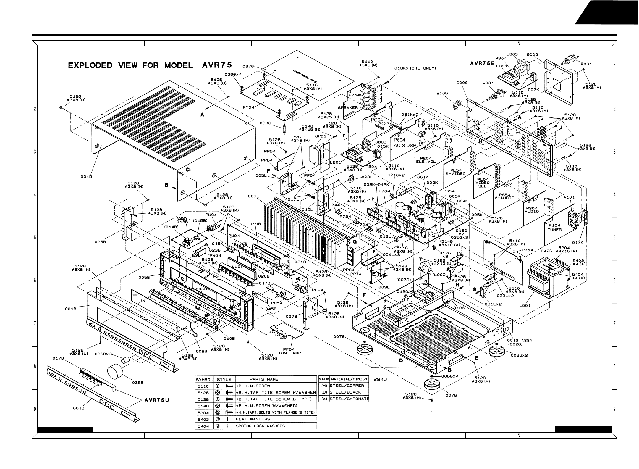
Harman Kardon
Dolby Digital Audio/Video Receiver
AVR75/85
AVR75 MECHANICAL EXPLODED VIEW (120V AND 230V)
BA
1
C
ED
F
G
H
I LMK
J
O
P
AVR75/85 PAGE 32-1of2
ABCDE
F
AVR75/85 PAGE 32 - 2 of 2
G
H
J
K
LMI
O
P
32
Page 33

Harman Kardon
Dolby Digital Audio/Video Receiver
AVR75 MECHANICAL PARTS LIST (120V & 230V)
AVR75/85
Ref.# Part # Description Qty.
001B 260J248360 FRONT ALMI PANEL (BLACK) N 1
001B 260J248350 FRONT ALMI PANEL (BLACK) U 1
005B 260J105015 FRONT MOLD CHASSIS 1
006B 259J118010 SPACER FOR HINGE BUTTON 1
008B 260J158350 WINDOW 1
010B 260J270010 FUNCTION HINGE BUTTON 1
011B 51280308M0 B.H. TAP. SCREW FUNCTION 7
HINGE BUTTON
013B 260J270520 BUTTON POWER BUTTON KIT 1
014B 260J270050 POWER BUTTON 1
015B 260J355020 POWER BUTTON LENS 1
017B 260J270020 MODE HINGE BUTTON (N) 1
017B 260J270120 MODE HINGE BUTTON (U) 1
019B 183J271022 FL HOLDER 1
020B 056J122010 STICKER ADHESIVE FOR FL 1
021B 4220005040 CLAMPER FOR FLAT CABLE 1
022B 51280308M0 B.H. TAP. SCREW FUNCTION 16
PCB
023B 183J010010 SCREW PHONE PCB 1
024B 51280308M0 B.H. TAP. SCREW FOR POWER 2
SWITCH PCB
025B 264J160040 FRONT LEFT SIDE BRACKET 1
026B 51280308M0 B.H. TAP. SCREW FRONT LEFT 4
SIDE BRACKET
027B 264J160050 BRACKET FRONT RIGHT 1
SIDE BRACKET
028B 51280308M0 B.H. TAP. SCREW FRONT RIGHT 4
SIDE BRACKET
030B 51280308U0 B.H. TAP. SCREW ALMI PANEL 3
DOWN SIDE
031B 51280308M0 B.H. TAP. SCREW ALMI PANEL 1
UP CENTER
033B 51280308M0 B.H. TAP. SCREW FRONT PANEL 4
ASSEMBLY
035B 063J154180 MAIN VOL KNOB 1
036B 042J154180 TONE VOL KNOB 3
041B 51280308M0 B.H. TAP. SCREW FOR CLAMPER 1
045B 288J123010 CONTACTOR 1
001D 264J257110 LID TOP COVER BLACK 1
005D 51260308U0 B.T.SCREW(W/W) TOP COVER 3
REAR
006D 5126030SU0 B.T.SCREW(W/W) TOP COVER 8
SIDE
001G 264J105500 MAIN CHASSIS ASSY 1
Ref.# Part # Description Qty.
002G 264J105010 MAIN CHASSIS 1
003G 030J114010 STOPPER 1
006G 227J056010 BUFFER PEFU SHEET 4
007G 183J057010 LEG (FRONT) 2
008G 183J057110 LEG (REAR) 2
009G 51280308M0 B.H. TAP. SCREW LEG 4
010G 264J160010 TRANSF. BRACKET 1
011G 51280308M0 B.H. TAP. SCREW TRANSF. 2
BRACKET
012G 52040410M0 H.HEAD BOLT S.F. TRANSF. 4
013G 260J271010 HOLDER SUB TRANSF BASE 1
014G 51280325U0 B.H. TAP. SCREW SUB TRANSF 2
015G 51280308M0 B.H. TAP. SCREW DENGEN 2
PCB
016G 2218271020 HOLDER VERTICAL PCB SUPPORT 7
017G 054J101020 MAIN PCB SUPPORT 8
018G 278J861010 FUSE LABEL T1.6A 250V 4
020G 54040402A0 SPRING WASHER FOR TRANSF FIX 4
021G 54020401A0 FLAT WASHER 4
P. FOR TRANSF. FIX
03OG 136J101020 SUPPORT FOR CONNECTOR PCB 1
031G 51280410U0 B.H. TAP. SCREW FOR EMC 1
PART LOCK
031G 51280410U0 B.H. TAP. SCREW FOR EMC 1
PART LOCK
035G 140S056040 BUFFER FOR MAIN PCB 2
037G 288J053012 COVER 1
039G 329K101010 SUPPORT FOR COVER 4
041G 51100306M9 B.H.M. SCREW MAIN PCB+SUB 2
PCB
042G 288J861013 TRANS LABEL 1
900G 294J250020 REAR PANEL (N) 1
900G 294J250010 REAR PANEL (U) 1
901G 51280308M0 B.H. TAP. SCREW RCA 19
902G 51100306M9 B.H.M. SCREW FOR CONTRACTOR 5
903G 51100308A9 B.H.M. SCREW CONNECT PCB 5
905G 51280308M0 B.H. TAP. SCREW REAR PANEL 6
906G 51280308M0 B.H. TAP. SCREW SPEAKER TERMINAL 3
907G 51280308M0 B.H. TAP. SCREW AC OUTLET 2
907G 51280308M0 B.H. TAP. SCREW AC OUTLET 2
910G 450H259010 BUSHING AC CODE BUSH 2271 1
915G 260J861010 “UL, CUL LABEL” 1
33
Page 34

Harman Kardon
Dolby Digital Audio/Video Receiver
AVR75 MECHANICAL PARTS LIST (120V &230V) continued
AVR75/85
Ref.# Part # Description Qty.
920G 95109111D0 FACTORY ID TSK LABEL 1
001L 288J267010 MAIN HEATSINK 1
002L 51480310A9 F.WASHER SCREW POWER 12
TR
003L 51480310A9 F.WASHER SCREW REGULATOR 3
TR
004L 288J107010 SHEET FOR POWER TR 3
005L 264J160020 HEAT SINK LEFT SIDE BRACKET 1
006L 51280308M0 B.H. TAP. SCREW LEFT SIDE 2
BRACKET
009L 264J160030 HEAT SINK RIGHT SIDE BRACKET 1
010L 51280308M0 B.H. TAP. SCREW RIGHT SIDE 2
BRACKET
013L 261J104010 MAIN PCB RETAINER 2
014L 51100306M9 B.H.M. SCREW MAIN PCB 2
RETAINER
015L 264J160060 HEATSINK CENTER BRACKET 1
016L 51100306M9 B.H.M. SCREW CENTER 2
BRACKET
017L 090J101010 SURROUND PCB SUPPORT 2
018L 51480315M9 F.WASHER SCREW SURROUND PACK 2
020L 287S005010 CLAMPER FOR CORD 1
025L 51260308M0 B.T.SCREW(W/W) MAIN PCB 4
KARI
026L 51260308M0 B.T.SCREW(W/W) MAIN PCB 2
ASSEMBLY
027L 51280308M0 B.H. TAP. SCREW HEAT SINK 8
ASSEMBLY
028L 51280308M0 B.H. TAP. SCREW SIDE PCB 2
030L 51280308M0 B.H. TAP. SCREW MAIN PCB 2
ASSEMBLY
031L 288J160010 BRACKET FOR SUB PCB(1) 2
032L 51100306M9 B.H.M. SCREW BRACKET FOR 4
SUB PCB(1)
033E 288J160020 BRACKET FOR SUB PCB( 2) 2
034L 51100306M9 B.H.M. SCREW BRACKET FOR 2
SUB PCB(2)
QP01 HC10386030 STK401 IC 1
Ref.# Part # Description Qty.
Printed Circuit Boards
Part # PCB Type
P714 VOLTAGE AMP PCB
P604 AC-3/DAC PCB
P704 MAIN PCB
PS04 AUDIO FUNCTION PCB
PS54 AUDIO/VIDEO PCB
PE04 ELECTRONIC VOLUME CONTROL PCB
PC04 AC-3 CROSSOVER PCB
PU94 POWER SWITCH PCB
P754 SPEAKER TERMINAL PCB
PL04 VIDEO SELECTOR PCB
PY04 CONNECT PCB
PL54 S-VIDEO PCB
P104 TUNER PCB
PB04 STANDBY PCB
PP04 SURROUND AMP PCB
PU04 FRONT PCB
PU54 MASTER VOLUME PCB
PN54 SPEAKER PROTECT PCB
PF04 TONE CONTROL PCB
PL94 AUX IN
PW04 HEADPHONE PCB
34
Page 35
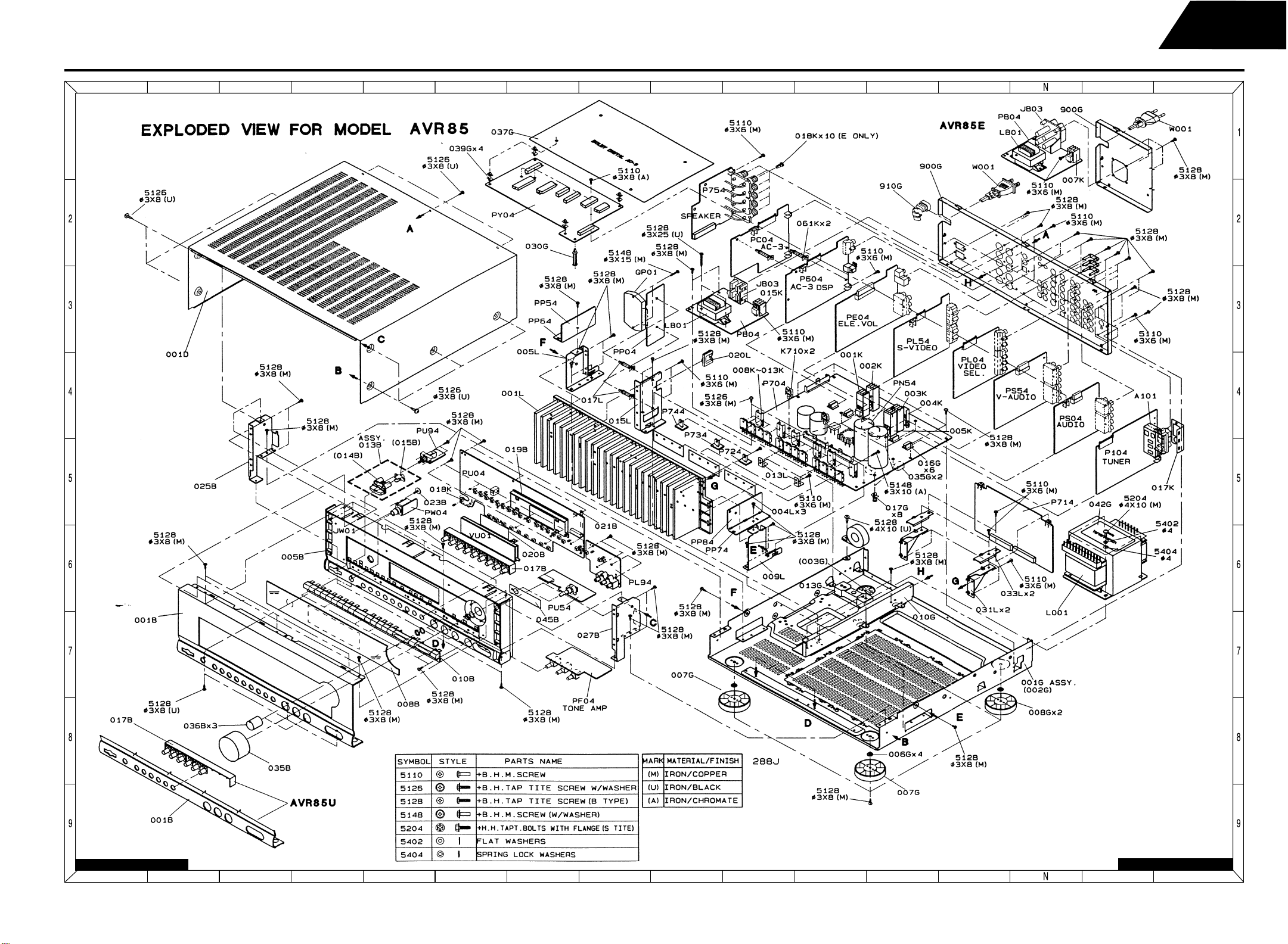
Harman Kardon
Dolby Digital Audio/Video Receiver
AVR75/85
AVR85 MECHANICAL EXPLODED VIEW (120V AND 230V)
BA
1
C
ED
F
G
H
I LMK
J
O
P
AVR75/85 PAGE 35-1of2
ABCDE
F
AVR75/85 PAGE 35 - 2 of 2
G
H
J
K
LMI
O
P
35
Page 36
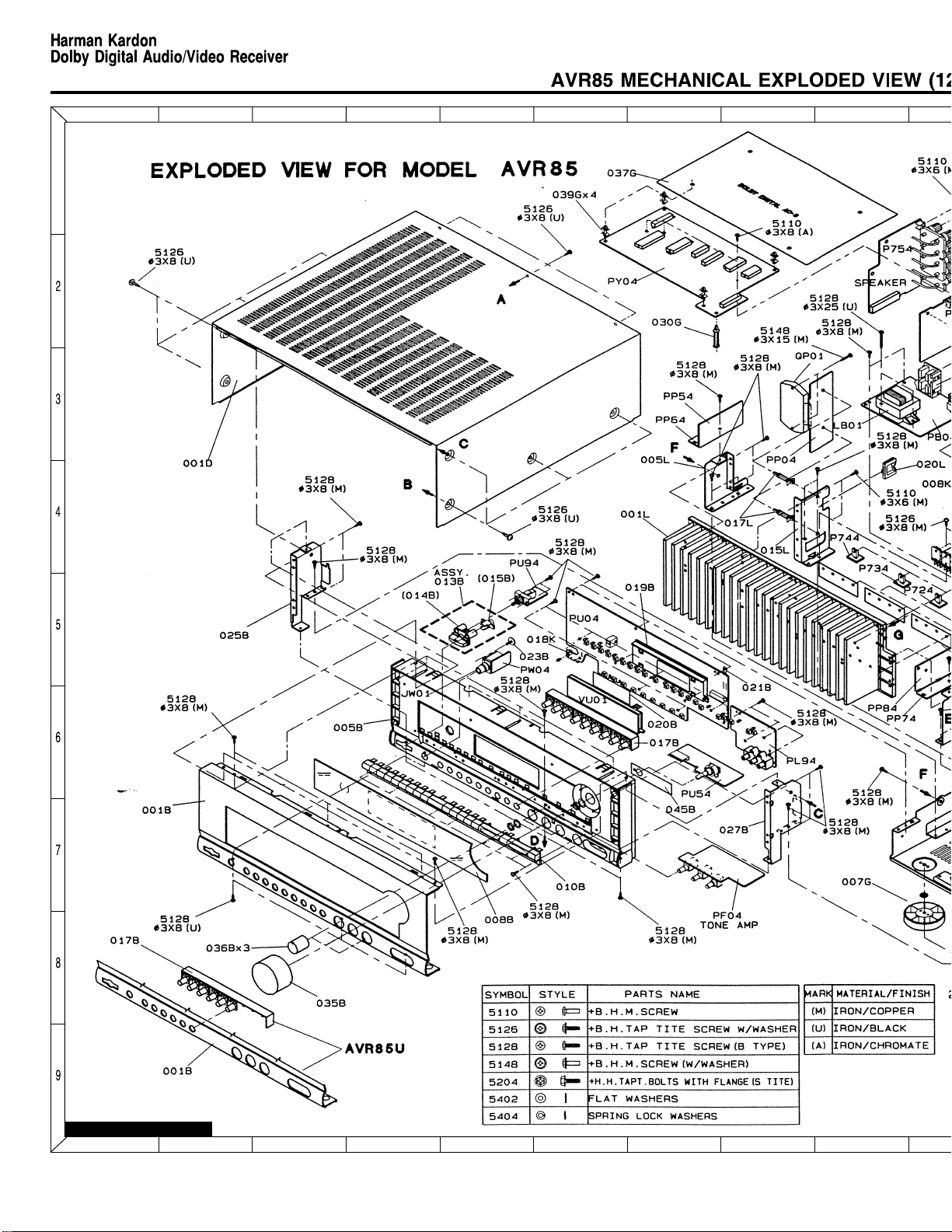
BA
1
C
ED
F
G
H
I
AVR75/85 PAGE 35 - 1 of 2
ABCDE
F
G
H
I
Page 37
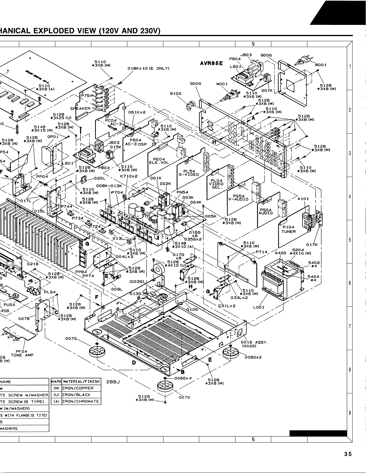
AVR75/85
G
G
H
I LMK
J
O
P
AVR75/85PAGE35-2of2
H
J
K
LMI
O
P
Page 38

Harman Kardon
Dolby Digital Audio/Video Receiver
AVR85 MECHANICAL PARTS LIST (120V & 230V)
AVR75/85
Ref.# Part # Description Qty.
001B 260J248320 FRONT PANEL BLACK 120V 1
260J248310 FRONT PANEL BLACK 230V 1
0058 260J105015 CHASSIS, FRONT MOLD 1
008B 260J158312 WINDOW 1
010B 260J270010 BUTTON, FUNCTION HINGE 1
011B 51280308M0 SCREW, B.H. TAP. FUNCTION HINGE 7
BUTTON
013B 260J270520 BUTTON, POWER BUTTON KIT 1
014B 260J270050 BUTTON, POWER BUTTON 1
015B 260J355020 LENS, POWER BUTTON LENS 1
017B 260J270020 BUTTON, MODE HINGE BLACK 120V 1
260J270120 BUTTON, MODE HINGE BLACK 230V 1
019B 183J271022 HOLDER, FL HOLDER 1
020B 056J122010 STICKER ADHESIVE FOR FL 1
021B 4220005040 CLAMPER FOR FLAT CABLE 1
022B 51280308M0 SCREW, B.H. TAP. FUNCTION PCB 16
023B 183J010010 SCREW, PHONE PCB 1
024B 51280308M0 SCREW, B.H. TAP. FOR 2
POWER SWITCH
025B 264J160040 BRACKET, FRONT LEFT SIDE 1
026B 51280308M0 SCREW, B.H. TAP FRONT LEFT SIDE 4
027B 264J160050 BRACKET, FRONT RIGHT SIDE 1
028B 51280308M0 SCREW, B.H. TAP FRONT 4
RIGHT SIDE BRACKET
030B 51280308U0 SCREW, B.H. TAP. ALUMINUM 3
PANEL DOWN SIDE
031B 51280308M0 SCREW, B.H. TAP. ALUMINUM 1
PANEL UP CENTER
033B 51280308M0 SCREW, B.H. TAP. FRONT PANEL 4
ASSEMBLY
035B 063J154180 KNOB, MAIN BLACK KNOB 1
036B 04J154022 KNOB, VOLUME KNOB 3
041B 51280308M0 SCREW, B.H. TAP. FOR CLAMPER 1
045B 288J123010 CONTACTOR 1
001D 264J257110 LID, TOP COVER BLACK 1
005D 51260308U0 SCREW, B.T. (W/W) TOP COVER 3
REAR
006D 51260308U0 SCREW, B.T. (W/W) TOP COVER 8
SIDE
001G 264J105500 CHASSIS, MAIN CHASSIS ASSEMBLY 1
002G 264J105010 CHASSIS, MAIN CHASSIS 1
003G 030J114010 STOPPER 1
Ref.# Part # Description Qty.
006G 227J056010 BUFFER, PEFU SHEET 4
007G 183J057010 LEG, FRONT 2
008G 183J057110 LEG, REAR 2
009G 51280308M0 SCREW, B.H. TAP. LEG 4
010G 264J160010 BRACKET, TRANSFORMER 1
011G 51280308M0 SCREW, B.H. TAP. TRANSFORMAER 2
BRACKET
012G 5204010M0 BOLT, H. HEAD S.F. 4
TRANSFORMER
013G 260J271010 HOLDER, SUB TRANSFORMER 1
BASE
014G 51280325U0 SCREW, B.H. TAP. SUB 2
SUB TRANSFORMER
015G 51280308M0 SCREW, B.H. TAP. 2
DENGEN PCB
016G 2218271020 HOLDER, VERTICAL PCB SUPPORT 7
017G 054J101020 SUPPORT, MAIN PCB SUPPORT 8
018G 278L861010 LABEL, FUSE LABEL T1.6A 250V 4
020G 54040402A0 SPRING WASHER, FOR 4
TRANSFORMER FIX
021G 54020401A0 FLAT WASHER P. 4
WASHER FOR TRANSFORMER FIX
030G 136J101020 SUPPORT, FOR CONNECTOR PCB 1
013G 51280410U0 SCREW, B.H. TAP. FOR EMC 1
PART LOCK 120V & 230V
035G 140S056040 BUFFER, FOR MAIN PCB 2
037G 288J053012 COVER 1
039G 329K101010 SUPPORT FOR COVER 4
041G 51100306M9 SCREW, MAIN PCB+SUB 2
042G 288J861013 LABEL, TRANSFORMER LABEL 1
900G 278J250222 REAR PANEL 120V 1
278J250212 REAR PANEL 230V 1
901G 51280308M0 SCREW, B.H. TAP. RCA 20
902G 51100306M9 SCREW, B.H.M. FOR CONTACTOR 5
903G 51100308A9 SCREW, B.H.M. CONNECT PCB 5
905G 51280308M0 SCREW, B.H. TAP. 6
REAR PANEL
906G 51280308M0 SCREW, B.H. TAP. 3
SPEAKER TERMINAL
907G 51280308M0 SCREW, B.H. TAP. (120V) 4
AC OUTLET
SCREW, B.H. TAP. (230V) 2
AC OUTLET
910G 450H259010 BUSHING 1
AC CODE BUSH 2271
36
Page 39

Harman Kardon
Dolby Digital Audio/Video Receiver
AVR85 MECHANICAL PARTS LIST (120V & 230V) continued
AVR75/85
Ref.# Part # Description Qty.
915G 260J861010 LABEL, UL, CUL LABEL 1
920G 95109111D0 LABEL, FACTORY ID TSK LABEL 1
001L 288J267010 HEATSINK, MAIN HEATSINK 1
002L 51480310A9 SCREW, F. WASHER 12
POWER TRANSFORMER
003L 51480310A9 SCREW, F. WASHER 3
REGULATOR TRANSFORMER
004L 288J107010 SHEET FOR POWER TRANSISTORS 3
005L 264J160020 BRACKET, HEAT SINK 1
LEFT SIDE BRACKET
006L 51280308M0 SCREW, B.H. TAP. 2
LEFT SIDE BRACKET
009L 264J160030 BRACKET, HEAT SINK 1
RIGHT SIDE BRACKET
010L 51280308M0 SCREW, B.H. TAP. 2
RIGHT SIDE BRACKET
013L 261J104010 RETAINER 2
MAIN PCB RETAINER
014L 51100306M9 SCREW, B.H.M. 2
MAIN PCB RETAINER
015L 264J160060 BRACKET 1
HEATSINK CENTER BRACKET
016L 51100306M9 SCREW, B.H.M. 2
CENTER BRACKET
017L 090J101010 SUPPORT 2
SURROUND PCB SUPPORT
018L 51480315M9 SCREW, F. WASHER 2
SURROUND PACK
020L 287S005010 CLAMPER 1
CLAMPER FOR CORD
025L 51260308M0 SCREW (W/W) B.T. 4
MAIN PCB KARI
026L 51260308M0 SCREW (W/W) B.T. 2
MAIN PCB ASSEMBLY
027L 51280308M0 SCREW, B.H. TAP. 8
HEAT SINK ASSEMBLY
028L 51280308M0 SCRWE, B.H. TAP. 2
SIDE PCB
030L 51280308M0 SCREW, B.H. TAP. 2
MAIN PCB ASSEMBLY
031L 288J160010 BRACKET 2
BRACKET FOR SUB PCB(1)
032L 51100306M9 SCREW, B.H.M. 4
BRACKET FOR PCB(1)
033L 288J160020 BRACKET 2
BRACKET FOR SUB PCB(2)
034L 51100306M9 SCREW, B.H.M. 2
BRACKET FOR SUB PCB(2)
QP01 HC10386030 STK401 IC 1
Ref.# Part # Description Qty.
L001 TS60513110 POWER TRANSFORMER (120V) 1
TS60513120 POWER TRANSFORMER (230V) 1
LB01 TS14823240 STANDBY TRANSFORMER (230V) 1
TS14823230 STANDBY TRANSFORMER (120V) 1
W001 YC01900260 AC POWER CORD (120V) 1
YC01800790 AC POWER CORD (230V) 1
JB03 YJ04002040 AC ACCESSORY JACK (120V) 1
YJ04002080 AC ACCESSORY JACK (230V) 1
L002 FC50380010 FERRITE CHOKE 1
015K 009D267010 HEATSINK FOR QB01 1
Printed Circuit Boards
Part # PCB Type
P714 VOLTAGE AMP PCB
P604 AC-3/DAC PCB
P704 MAIN PCB
PS04 AUDIO FUNCTION PCB
PS54 AUDIO/VIDEO PCB
PE04 ELECTRONIC VOLUME CONTROL PCB
PC04 AC-3 CROSSOVER PCB
PU94 POWER SWITCH PCB
P754 SPEAKER TERMINAL PCB
PL04 VIDEO SELECTOR PCB
PY04 CONNECT PCB
PL54 S-VIDEO PCB
P104 TUNER PCB
PB04 STANDBY PCB
PP04 SURROUND AMP PCB
PU04 FRONT PCB
PU54 MASTER VOLUME PCB
PN54 SPEAKER PROTECT PCB
PF04 TONE CONTROL PCB
PL94 AUX IN
PW04 HEADPHONE PCB
37
Page 40

Harman Kardon
Dolby Digital Audio/Video Receiver
AVR75/85
AVR75/85 ELECTRICAL PARTS LISTS
REF. N0. Part No. Description Qty.
General Miscellaneous
WB01 YB00182170 CONNECTIVE CORD EHR-3P 1
WF01 YB00620140 “CONNECTIVE CORD 12P 1
WP01 YB00331070 CONNECTIVE CORD UP-3P 1
WU02 YB00480330 CONNECTIVE CORD UP-7P 1
WU91 YB00501450 CONNECTIVE CORD 1
WU92 YB00071960 CONNECTIVE CORD UP-3P 1
WV51 YB00331180 CONNECTIVE CORD JY16(PY04)- 1
WW02 YB00550780 CONNECTIVE CORD EHR-5P 1
WY01 YB00451340 CONNECTIVE CORD 8P 1
W602 YB00451350 CONNECTIVE CORD UP-7P 1
W760 YB00122870 CONNECTIVE CORD VHR-5P 1
JB09(PB04)-JY11(PY04)
JF01(PF04)-JY15(PY04), JC02"
JP01(PP04)-JV57(PE04)
JU02(PU04)-JB04(PB04)
JB10-JU92-JN82-JY14
JU91(PU94)-JU06(PU04)
J701(P714)XJ804
JW02(PW04)-J706(P704)
JY10(PY04)-JL92(PL94)
J601(P604)-JU05(PU04)
J761(P754)-J803(P704)
PCB - PB04, Standby
REF. N0. Part No. Description Qty.
RB08 GD05103161 RESISTOR 10K OHM +- 5% 1/6W 1
Transistor
QB02 HT420331E1 ! 2SD2033(E) 12OV 1.8W ROHM 1
Miscellaneous
JB01 YJ08000581 JACK ! FUSE CLIP 20MM 1
JB01, 02 YJ08000170 JACK ! FUSE CLIP 20MM 2
JB02 YJ08000591 JACK ! FUSE CLIP 20MM 1
JB03 YJ04002080 JACK ! AC OUTLET 2P (N) 1
JB03 YJ04002040 JACK ! 2P AC OUTLET (CCT1304-0212) 1
JB04 YP06006670 PLUG 2MM PITCH UP CONNECTOR 7PIN 1
JB05, 06 YP04000760 PLUG CONNECTOR 2P B3P-VH 2
JB07 YL01010241 GND TERMINAL FOR PCB 1
JB09 YP0600383X PLUG B3B-EH 3P RADIAL TAPING 1
JB10 YP06006931 PLUG UP-3P CONNECTOR 1
LB01 TS14823240 # POWER TRANSF. STANDBY EU 230V 1
LB01 TS14823230 # POWER TRANSF. STANDBY USA 120V 1
LB02 LY10240240 RELAY # VS24MB-NR TV-8 1
015K 009D267010 HEATSINK FOR QB01 1
016K 51100306M9 B.H.M. SCREW FOR QB01+015K 1
SEMKO LISTED
Capacitors
CB01 EA47703516 ELECTROLY CAP 470UF 35V 1
CB02 EA10606311 ELECT. CAP. 10UF M 63V 1
CB03 EA47603511 ELECT. CAP. 47UF M 35V 1
CB05 EA47705016 ELECT. CAP. 470UF/50V 1
CB06 EA47603511 ELECTROLY CAP. 47UF 35V 1
CB07, 08 DK18103311 CERAMIC CAP. 0.01UF Z 50V 2
CB09 DK17103847 CERAMIC CAP. # 0.01UF 1
CB10 EA10606311 ELECT. CAP. 10UF M 63V 1
Diodes
DB01, 02, HD20002711 DIODE 1D3 1A/200V 4
03, 04
DB05 HD33301001 ZENER DIODE MTZJ33D 33V 1
DB06 HD30821001 ZENER DIODE NTJ8.2C 8.2V 1
DB07, 08 HD20002711 DIODE 1D3 1A/200V 2
Fuses
FB01 FS10400860 FUSE # 8A 250V (218004) 1
FB01 FS10630540 FUSE # 6.3A 250V SM6.3 1
FB02, 03 FS20250201 FUSE # T2.5A/250V SLO-BLO EU 230V 2
SLO-BLO EU 230V
SLO-BLO USA 120V
Integrated Circuit
QB01 HC38905320 IC ! PQ05RR1 5V 1A REGULATOR 1
Resistors
RB01 GG0510014X RESISTOR ! 10 OHM +- 5% 1/4W 1
RB03 GA05471010 RESISTOR 470 OHM 1W 1
RB04, 05 GD05101161 RESISTOR 100 OHM J 1/6W 2
RB07 RC10225820 RESISTOR ! 2.2M OHMS K 1/2W 1
PCB - PC04, AC-3 Crossover
Capacitors
CC01, 02 DF15104351 FILM CAP. 0.1UF J 50V 4
03, 04
CC05, 06 DA15220111 CERAMIC CAP. 22PF 2
CC07, 08, 09, EJ10601611 ELECTROLY CAP 10UF 16V 6
10, 11, 12
CC13, 14 DF15104351 FILM CAP 0.1UF J 50V 4
15, 16
CC17, 18, 19 EJ10601611 ELECTROLY CAP 10UF 16V 6
20, 21, 22
CC23, 24 DA15220111 CERAMIC CAP 22PF 50V 2
CC25, 26 EJ10601611 CAP 10UF 16V 2
CC27, 28 DA15220111 CERAMIC CAP 22PF 50V 2
CC29, 30, 33 EJ10601611 ELECTROLY CAP 10UF 16V 6
34, 35, 36
CC31, 32 DF15104351 FILM CAP 0.1UF J 50V 2
CC37 DA15220111 CERAMIC CAP 22PF 50V 1
CC38 DA15100121 CERAMIC CAP 10PF 1
CC39, 42, 45 EJ10601611 CAP 10UF 16V 5
47, 49
CC40 DF15104351 FILM CAP 0.1UF J 50V 1
CC41 DF15823311 FILM CAP 0.082 J 50V 1
CC43 DF15223351 “FILM CAP 0.022UF, J, M, 50V” 1
CC44 DF15154351 “FILM CAP 0.15UF, J, T, 50V” 1
CC46 DA15100121 CERAMIC CAP 10PF 1
CC48 DA15220111 CERAMIC CAP 22PF 50V 1
CC52, 53 EA10701611 CAP 100UF 16V 2
CC54, 55, 56 DK18103311 CERAMIC CAP 0.01UF Z 50V 17
57, 58, 59,
62, 63, 64,
65, 66, 67,
70, 71, 75,
76, 77
38
Page 41

Harman Kardon
Dolby Digital Audio/Video Receiver
REF. N0. Part No. Description Qty.
AVR75/85
REF. N0. Part No. Description Qty.
CC79 EA10601611 CAP 10UF 16V 1
CC80 EJ10601611 CAP 10UF 16V 1
Integrated Circuits
QC01, 02, 03 HC10008090 IC NJM4558DD DUAL OP-AMP 10
04, 05, 06,
07, 08, 09,
10
QC11 HC10123090 IC NJU7311L ANALOG SWITCH 1
QC12 HC10008090 IC NJM4558DD DUAL OP-AMP 1
Resistors
RC01, 02, 03, GD05223161 RESISTOR 22K OHM +- 5% 1/6W 4
04
RC05, 06 GD05102161 RESISTOR 1K OHM 5% 1/6W 2
RC07, 08, 09, GD05104161 RESISTOR 100K OHM J 1/6W 4
10
RC11, 12 GD05103161 RESISTOR 10K OHM J 1/6W 2
RC13, 14 GD05102161 RESISTOR 1K OHM J 1/6W 2
RC15, 16 GD05223161 RESISTOR 22K OHM J 1/6W 2
RC17, 18, 19, GD05104161 RESISTOR 100K OHM J 1/6W 6
20, 21, 22
RC23, 24, 25, GD05103161 RESISTOR 10K OHM J 1/6W 11
26, 27, 28,
29, 30, 31,
32, 36
RC33, 34, 38, GD05104161 RESISTOR 100K OHM J 1/6W 5
39, 40
RC35 GD05223161 RESISTOR 22K OHM J 1/6W 1
RC37 GD05102161 RESISTOR 1K OHM J 1/6W 1
RC41 GD05103161 RESISTOR 10K OHM J 1/6W 1
RC42 GD05822161 RESISTOR 8.2K OHM 5% 1/6W 1
RC43, 47, 48 GD05183161 RESISTOR 18K OHM 5% 1/6W 3
RC44 GD05562161 RESISTOR 5.6K OHM J 1/6W 1
RC45 GD05331161 RESISTOR 330 OHM J 1/6W 1
RC46, 49, 52 GD05104161 RESISTOR 100K OHM J 1/6W 5
55, 58
RC50, 51 GD05273161 RESISTOR 27K OHM 5% 1/6W 2
RC53, 56, 57 GD05103161 RESISTOR 10K OHM J 1/6W 6
62, 63, 64
RC54 GD05682161 RESISTOR 6.8K OHM J 1/6W 1
Miscellaneous
JC01 YP06020870 PLUG 17P A1 1
JC02 YP06007150 PLUG 2MM PITCH SIDE CONNECTOR 5P 1
JC03, 04, 05 YL01010140 TERMINAL M1698 GND TERMINAL 3
WITH M3
PCB - PW04, Headphone
Capacitors
CW09, 10, 11 DA17103111 CERAMIC CAP. 0.01UF M 16V 3
Miscellaneous
JW01 YJ01004240 H.P. JACK HLJ2307-01-3160 1
JW02 YP0601045X PLUG B5B-EH 5P RADIAL TAPING 1
WW01 YB00152110 CONNECTIVE CORD 1P 150 MM 1
PCB PU04, Front
Capacitors
CU01, 09 DA17223111 CERAMIC CAP. 0.022UF TP050F223Z 2
CU02 EX22300531 BIG ELECT. CAP 0.022 F 5.5V 1
CU03 EJ47601011 ELECT. CAP. 47UF/10V 1
CU04 DA17223111 CERAMIC CAP. 0.022UF TP050F223Z 1
CU05, 08 DD38104011 CERAMIC CAP. 0.1 UF Z 50V 2
CU10 EJ22700611 ELECT. CAP. 220UF/6.3V 1
CU14, 15 DA16102111 CERAMIC CAP. 1000PF K 50V B 2
Diodes/LEDs
DU01, 02, 03 HD20029211 DIODE 1SS132 3
DU07, 08, 09 HD20002001 “DIODE 1SS176, MA165, 1SS254 30V 0.1A” 12
10, 11, 12,
13, 14, 15,
16, 17, 18
DU19 HI10062321 L.E.D. LT3D8B RED 30 1
DU20 HI10099320 L.E.D. GL3ED8 SHARP 1
DU21, 22 HD20002000 “DIODE 1SS176, MA165, 1SS245 30V 0.1A” 2
DU30, 31, 32, HI10095321 L.E.D. LT3K44B GREEN 30MA 9
33, 34, 35,
36, 37, 38
DU40, 41, 42, HI10095321 L.E.D. LT3K44B GREEN 30MA 7
43, 45, 46,
47
Integrated Circuits
QU01 HU288JT00F MICROPROCESSOR TMP87CP71F-6630 1
QU05 HC754100B0 IC 74HC541 DIP 3 STATE BUFFER/ 1
Resistors
DU39 GD05151161 RESISTOR 150 OHM +- 5% 1
RU01, 02, 03, GD05152161 RESISTOR 1.5K OHM +- 5% 1/6W 5
04, 05
RU06, 07, 08, GD05222161 RESISTOR 2.2K OHM +- 5% 1/6W 5
09, 10
RU11, 12, 13, GD05332161 RESISTOR 3.3K OHM +- 5% 1/6W 5
14, 15
RU16, 17, 18, GD05332161 RESISTOR 6.8K OHM +- 5% 1/6W 5
19, 20
RU21, 22, 23, GD05103161 RESISTOR 10K OHM +- 5% 1/6W 10
24, 25, 26,
27, 28, 29,
30
RU36, 37 GD05151161 RESISTOR 150 OHM +- 5% 1/6W 2
RU39 GD05101161 RESISTOR 100 OHM +- 5% 1/6W 1
RU40, 43, 44, GD05103161 RESISTOR 10K OHM +- 5% 1/6W 11
45, 48, 51,
53, 54, 59,
64, 65
RU41, 49, 50, GD05473161 RESISTOR 47K OHM +- 5% 1/6W 7
52, 55, 60,
67
RU42 GD05183161 RESISTOR 18K OHM +- 5% 1/6W 1
RU46 GD05471161 RESISTOR 470 OHM +- 5% 1/6W 1
RU47 GD05221161 RESISTOR 220 OHM +- 5% 1/6W 1
RU56, 57, 58 GD05182161 RESISTOR 1.8K OHM +- 5% 1/6W 3
RU63 GD05100161 RESISTOR 10 OHM +- 5% 1/6W 1
RU66 GD05303161 RESISTOR 330 OHM +- 5% 1/6W 1
RU68 GG0501014X RESISTOR 1 OHM +- 5% 1/4W 1
TAIYO YUDEN
SUPER CAPACITOR
TAIYO YUDEN
8BIT U-COM
LINE DRIVER
39
Page 42

Harman Kardon
Dolby Digital Audio/Video Receiver
REF. N0. Part No. Description Qty.
AVR75/85
REF. N0. Part No. Description Qty.
RU69 GD05104161 RESISTOR 100K OHM +- 5% 1/6W 1
Switches
SU01, 02, 03, SP0101128X PUSH SWITCH TACK SWITCH 26
04, 06, 07, ALPS-SKHVAE
08, 09, 10,
11, 12, 13,
14, 15, 17,
18, 19, 20,
22, 23, 24,
25, 26, 28,
29, 30
Transistors
QU02 BA20001001 “SEMICON.COMP DTC114ES/UN4211 1
QU03 BA10001001 “SEMICON.COMP DTA114ES/UN4111 1
QU04, 08, 14 BA20002001 “SEMICON.COMP DTC144ES/UN4213 3
QU06, 07, 10 HT30001001 “TRANSISTOR C536SP, C2458, 4
12 C3311,C1740S”
QU09 HT10001001 “TRANSISTOR A608SP, A1048, 1
QU11, 15 BA10002001 “SEMICON.COMP DTA144ES/ 2
QU13 BA10003211 SEMICON.COMP DIGITAL TRANSISTOR 1
10K, 10K”
10K, 10K”
47K, 47K”
A1309, A933S”
UN4113 47K, 47K”
DTA114TS
Miscellaneous
JU01 YJ07011160 JACK 9604S-23P 1
JU02 YP06007170 PLUG W-P7907 1
JU03 YJ06030640 JACK TSK-B04X-A1 1
JU04 YP06006290 PLUG S6B-XH-A 1
JU05 YP06001260 PLUG 2MM PITCH UP CONNECTOR 8PIN 1
JU06 YP06006931 PLUG UP-3P CONNECTOR 1
PU04 WA288J5010 PWB INSERT+CHIP ! UCOM/ 1
QU16 HW10001210 PHOTO UNIT IR RECEIVER 1
VU01 HQ31210060 DISPLAY UNIT FIP12DM8R NEC 1
XU01 FQ08004011 CERAMIC VIB.CST8.0MHZ (MT) TAPING 1
018K 152J118030 SPACER FOR DU20 LED SPACER 1
FUNCTION-SW PCB
RPM-670CBR H-15MM
12WGIT 16SEG
Integrated Circuit
QL91 HC10008090 IC NJM4558DD DUAL OP-AMP 1
Resistors
RL91 GD05100161 RESISTOR 10 OHM +- 5% 1/6W 1
RL92 GD05750161 RESISTOR 75 OHM +- 5% 1/6W 1
RL93, 94 GD05473161 RESISTOR 47K OHM +- 5% 1/6W 2
RL95, 96 GD05151161 RESISTOR 150 OHM +- 5% 1/6W 2
RU38 GD05100161 RESISTOR 10 OHM +- 5% 1/6W 1
Switches
SU05, 06, 21 SP0101128X PUSH SWITCH TACK SWITCH 3
ALPS-SKHVAE
Miscellaneous
WL91 SP0101128X CONNECTIVE CORD BOARD IN/#18 OFC 1
PCB -PU54, Master Volume
Capacitors
CU71 DA16102111 CERAMIC CAP. 1000PF K 50V B 1
CU72 DA16102111 CERAMIC CAP. 1000PF K 50V B 1
Diode
DU71 HD20002000 “DIODE 1SS176, MA165, 1SS254 30V 0.1A” 1
Miscellaneous
JU51 YP06020740 PLUG TSK-B04P-A1 1
Transistors
QU71, 72 HT30001001 “TRANSISTOR C536SP, C2458, 2
Resistors
RU71, 72 GD05104161 RESISTOR 100K OHM +- 5% 1/6W 2
RU73, 74 GD05104161 RESISTOR 220K OHM +- 5% 1/6W 2
C3311, C1740S”
PCB - PL94, Aux In
Capacitor
CL91, 93, 94 EJ10601611 ELECT. CAP. 10UF/16V 3
CL92 EJ22601611 ELECT. CAP. 22UF/16V 1
CL97, 98 DA16681111 CERAMIC CAP. 680PF K 50V 2
LEDs
DU48 HI10095321 L.E.D. LT3K44B GREEN 30MA 1
DU49 HI10095321 L.E.D. LT3K44B GREEN 30MA 1
Miscellaneous
JL91 YT02030390 TERMINAL AUX YKC21-XXXX 1
JL92 YP06007260 PLUG UP-8P 1
JU52 YJ06008860 JACK 06JQ-ST 1
PL94 WA288J5040 INSERT+CHIP ! AUX IN PCB 1
Switch
SU75 SR02010040 ROTARY SWITCH ENCODER EC16B40B0 1
Miscellaneous
WU71 YB00152520 CONNECTIVE CORD 1P CORD RUG-NON 1
PCB - P724
Miscellaneous
J717 YP06006931 CONNECTIVE PLUG UP 3P 1
Q725 HT33423100 TRANSISTOR 2SC3423 O 1
40
Page 43

Harman Kardon
Dolby Digital Audio/Video Receiver
REF. N0. Part No. Description Qty.
AVR75/85
REF. N0. Part No. Description Qty.
PCB - P734
Miscellaneous
718 YP06006931 CONNECTIVE PLUG UP 3P 1
Q726 HT33423100 TRANSISTOR 2SC3423 O 1
PCB - P744
Miscellaneous
719 YP06006931 CONNECTIVE PLUG UP 3P 1
QH13 HT33423100 TRANSISTOR 2SC3423 O 1
PCB - P714, Voltage Amp
Capacitors
CH01 EA476016Q1 ELECT. CAP. 47UF/16V MATSUSHITA 1
CH02 DK16681301 CERAMIC CAP. 680PF K 50V 1
CH02, C703 DD15680301 CERAMIC CAP. 68PF J CH 50V BLK 3
C704
CH03 DF15102351 FILM CAP. J, M, 1000 PF 50V 1
CH04, 05 EA477063Q6 ELECT. CAP. 470UF/63V MATSUSHITA 2
CH06 DD10030301 CERAMIC CAP. 3PF C CJ 50V BLK 1
CH07 DK16101301 CERAMIC CAP. 100PF K 50V 1
CH08 EA108006Q1 ELECT. CAP. 1000UF/6.3V MATSUSHITA 1
CH09, 11 EA106100Q1 ELECT. CAP. 10UF/100V MATSUSHITA 2
CH12, 13 DF15104351 “FILM CAP. 0.1UF, J, N, 50V” 2
CH15, 16 DD15220550 CERAMIC CAP. 22PF J 500V CH 2
C701, 702 EA476016Q1 ELECT. CAP. 47UF/16V MATSUSHITA 2
C703, 704 DK16681301 CERAMIC CAP. 680PF K 50V 2
C705, 706 DF15102351 “FILM CAP. 0.001UF, J, M, 50V” 2
C707, 708, EA477063Q6 ELECT. CAP. 470UF/63V MATSUSHITA 4
709, 710
C711, 712 DD10030301 CERAMIC CAP. 3PF C CJ 50V BLK 2
C713, 714 DK16101301 CERAMIC CAP. 100PF K 50V 2
C715, 716 EA108006Q1 ELECT. CAP. 1000UF/6.3V MATSUSHITA 2
C717, 718, EA106100Q1 ELECT. CAP. 10UF/100V MATSUSHITA 4
721, 722
C723, 724, DF15104351 “FILM CAP. 0.1UF, J, N, 50V” 4
725, 726
C740, 741, DD15220550 CERAMIC CAP. 22PF J 500V CH 4
742, 743
CN73 EJ10601611 ELECT. CAP. 10m F M 16V 1
CN74 EJ22700611 ELECT. CAP. 220m F M 6.3V 1
CN75 DK16102300 CERAMIC CAP. 1000PF K 50V 1
CW01, 02 EA105050Q1 ELECT. CAP. 1UF/50V 2
CW03, 04 EA475050Q1 ELECT. CAP. 4.7UF/50V 2
CW05, 06 EA106050Q1 ELECT. CAP. 10UF/50V 2
CW07, 08 EA227016Q1 ELECT. CAP. 220UF/16V 2
Diodes
D701, 702 HD20029051 DIODE S5688G 400V 1A 2
D703, 704 HD20002001 “DIODE 1S1555/2473/2076, DS448, MA150" 2
DH01 HD20029051 DIODE S5688G 400V 1A 1
DH02, DN74 HD20002001 “DIODE 1S1555/2473/2076, DS448, MA150" 2
Integrated Circuit
QW01 HC10016090 IC NJM4458D DUAL OP-AMP 1
Resistors
RH01 GD05331141 RESISTOR 330 OHM +- 5% 1/4W 1
RH02 GD05333141 RESISTOR 33K OHM +- 5% 1/4W 1
RH03, 04 GD05152141 RESISTOR 1.5K OHM +- 5% 1/4W 2
RH05, 06 GD05331141 RESISTOR 330 OHM +- 5% 1/4W 2
RH07 GD05271161 RESISTOR 270 OHM +- 5% 1/6W 1
RH08 NH0510214X FUSIBLE RESIST 1K OHM J 1/4W 1
RH09 GD05122141 RESISTOR 1.2K OHM +- 5% 1/4W 1
RH10 GD05333141 RESISTOR 33K OHM +- 5% 1/4W 1
RH11, 12, 13, NF0256114X FUSE RESISTOR 560 OHM G 1/4W 8
14, 15, 16,
17, 18
RH19, 20 GD05153141 RESISTOR 15K OHM +- 5% 1/4W 2
RH21, 22 NF0215114X FUSE RESISTOR 150 OHM G 1/4W 2
RH23, 24 NH05100142 FUSIBLE RESIST 10 OHM J 1/4W 2
R701, 702 GD05331141 RESISTOR 330 OHM +- 5% 1/4W 2
R703, 704 GD05333141 RESISTOR 33K OHM +- 5% 1/4W 2
R705 GD05152141 RESISTOR 1.5K OHM +- 5% 1/4W 1
R706, 707, GD05152141 RESISTOR 1.5K OHM +- 5% 1/4W 3
708
R709, 710, GD05331141 RESISTOR 330 OHM +- 5% 1/4W 4
711, 712
R713, 14 GD05271161 RESISTOR 270 OHM +- 5% 1/6W 2
R715, 716 NH0510214X FUSIBLE RESIST 1K OHM J 1/4W 2
R717, 18 GD05122141 RESISTOR 1.2K OHM +- 5% 1/4W 2
R719, 20 GD05333141 RESISTOR 33K OHM +- 5% 1/4W 2
R721, 722, NF0256114X FUSE RESISTOR 560 OHM G 1/4W 12
723, 724,
725, 726,
727, 728,
729, 730,
731, 732
R733, 734 NF0215114X FUSE RESISTOR 150 OHM G 1/4W 4
735, 736
R737, 738 GD05153141 RESISTOR 15K OHM +- 5% 1/4W 4
739, 740
R741, 742 NF0215114X FUSE RESISTOR 150 OHM G 1/4W 4
743, 744
R745, 746, NH05100142 FUSIBLE RESIST 10 OHM J 1/4W 4
747, 748
RN78, 79 GD05102161 RESISTOR 1K OHM +- 5% 1/6W 2
RW01, 02 GD05103161 RESISTOR 10K OHM +- 5% 1/6W 2
RW03, 04 GD05224161 RESISTOR 220K OHM +- 5% 1/6W 2
RW05, 06 GD05563161 RESISTOR 56K OHM +- 5% 1/6W 2
RW07, 08 GD05224161 RESISTOR 220K OHM +- 5% 1/6W 2
RW09, 10 GD05820161 RESISTOR 82 OHM +- 5% 1/6W 2
RW11, 12 GD05102161 RESISTOR 1K OHM +- 5% 1/6W 2
RW13, 14 NH05100142 FUSIBLE RESIST 10 OHM J 1/4W 2
Transistors
QH01, 02, 03 HT317751E1 TRANSISTOR 2SC1775A E RANK 9
Q701, 702,
703, 704,
705, 706
QH04, Q707, HT317401L1 TRANSISTOR 2SC1740S(R) 3
Q708
QH05, Q709, HF203731Y1 F.E.T. 2SK373-Y TPE2 3
710
QH06, 07 HT109701B1 TRANSISTOR 2SA970 (BL) TOSHIBA 6
Q711, 712,
713, 714
41
Page 44

Harman Kardon
Dolby Digital Audio/Video Receiver
REF. N0. Part No. Description Qty.
AVR75/85
REF. N0. Part No. Description Qty.
QH08, Q715, HT322401B1 TRANSISTOR 2SC2240 (BL) TPE2 TOSHIBA 3
716
QH09, 11, HT111242R0 “TRANSISTOR 2SA1124 (R,S)” 6
Q717, 718,
721, 722,
QH10, 12, HT326322R0 “TRANSISTOR 2SC2632 (R,S)” 6
Q719, 720
723, 724
QN71 BA20001001 “SEMICON.COMP DTC114ES/ 1
QN72 HT109331Q1 TRANSISTOR 2SA933S(Q) 1
QN73 HT317401L1 TRANSISTOR 2SC1740S(R) 1
QN74, 75 HT109331Q1 TRANSISTOR 2SA933S(Q) 2
QN76 BA10009211 SEMICON.COMP DTA144TS 1
UN4211 10K, 10K”
Miscellaneous
J701, 706 YP0601045X PLUG 85B-EH 2
J702 YP06019700 PLUG TAC-P20P-A1 1
J707 YL0101241X TERMINAL GND TERMINAL FOR PCB 1
J708, 709, YL01010241 TERMINAL GND TERMINAL FOR PCB 4
710, 712
J713 YP06019650 PLUG TAC-P15P-A1 1
J715 YP06019650 PLUG TAC-P15P-A1 1
J714, 716 YJ06020750 JACK TAC-P15X-A1 2
J720, 721 YL01010140 TERMINAL M1698 PWB GND 2
RP17, 18 GD05273161 RESISTOR 27K OHM +- 5% 1/6W 2
RP19, 20 GD05223161 RESISTOR 22K OHM +- 5% 1/6W 2
RP21, 22 GA05100010 RESISTOR 10 OHM +- 5% 1W 2
RP23, 24 GD05221161 RESISTOR 220 OHM +- 5% 1/6W 2
RP23, 23 GD05181161 RESISTOR 180 OHM +- 5% 1/6W 2
RP25, 26 GG0510116X RESISTOR 100 OHM +- 5% 1/6W 2
RP27 GD05682161 RESISTOR 6.8K OHM +- 5% 1/6W 1
RP28 GD05333161 RESISTOR 33K OHM +- 5% 1/6W 1
RP29 GD05100161 RESISTOR 10 OHM +- 5% 1/6W 1
RP99 GG0510014X RESISTOR 10 OHM J 1/4W 1
(AVR75/85 230V)
(AVR75/85 120V)
Transistors
QP02, 03 HT322402A1 TRANSISTOR 2SC2240 GR OR BL 2
QP04 HT109702A1 TRANSISTOR 2SA970 (GR) OR (BL) 1
TOSHIBA
TOSHIBA
Miscellaneous
JP01 YP06006931 PLUG CONNECTIVE PLUG UP 3P 1
LP01 ML08010030 AIR COIL SPK CHOCK COIL 1
LP02 ML08010030 AIR COIL SPK CHOCK COIL 1
WP02 YB00170880 CONNECTIVE CORD VHR-6P/SDN-6P 1
WP03 YB00170870 CONNECTIVE CORD 1P 170MM 1
VERTICAL TYPE
VERTICAL TYPE
TO J802(P704)
PCB - PP04, Surround Amp
Capacitors
CP01, 02 DK16222301 CERAMIC CAP. 2200PF K 50V 1
CP03, 04 EQ10606391 ELECT. CAP. 10UF M 63V 2
CP05, 06 EA10701611 ELECT. CAP. 100UF/16V 2
CP07, 08, DD11100301 CERAMIC CAP. 10PF D CH 50V 2
CP09, 10, 11, EJ22405011 ELECT. CAP. 0.22UF/50V 4
12
CP13, 15 EA10706311 ELECT. CAP. 100UF/63V 2
CP14 EA10706311 ELECT. CAP. 10UF M 63V 1
CP16 EA10606311 ELECT. CAP. 10UF M 63V 1
CP17 EJ22601011 ELECT. CAP. 22UF/10V 1
CP21, 22 DD15470301 CERAMIC CAP. 47PF J CH 50V BLK 2
Diodes
DP01, 02 HD20027011 DIODE HSS81TD 150V 150MA AXIAL TAPG. 2
Integrated Circuit
QP01 HC10386030 IC ! STK401-120 (70WX70W) POWER AMP 1
Resistors
RP01, 02, 16 GD05102161 RESISTOR 1K OHM +- 5% 1/6W 3
RP01, 02 GD05471161 RESISTOR 470 OHM +- 5% 1/6W 2
RP03, 04 GD05473161 RESISTOR 47K OHM +- 5% 1/6W 2
RP05, 06 GD05563161 RESISTOR 56K OHM +- 5% 1/6W 2
RP07, 08 GD05222161 RESISTOR 2.2K OHM +- 5% 1/6W 2
RP09, 10 GD05513161 RESISTOR 51K OHM +- 5% 1/6W 2
RP11, 12 GD10222050 RESISTOR 0.22 OHM +- 10% 5W 2
RP13, 14, 15 GG0510216X RESISTOR 1K OHM +- 5% 1/6W 3
PCB - PN54, Speaker Protect
Capacitors
CN81, 82 EJ10505011 ELECT. CAP. 1m F M 50V 2
CN83 DD38104011 CERAMIC CAP. 0.1 50V 1
Diodes
DN81, 82 HD20002001 DIODE 1SS176 2
Resistors
RN84, 87 GD05473161 RESISTOR 47K OHM J 1/6W 2
RN85 GD05104161 RESISTOR 100K OHM J 1/6W 1
RN86 GD05103161 RESISTOR 10K OHM +- 5% 1/6W 1
RN88 GD05101161 RESISTOR 100 OHM J 1/6W 1
Transistors
QN81 BA10001001 “SEMICON.COMP DTA114ES/ 1
QN82, 83 HT322402A1 TRANSISTOR 2SC2240 GR OR BL 2
Miscellaneous
JN81 YJ06019130 JACK 1
JN82 YP06007130 3P PLUG 1
QN84 HC10042050 IC TA7317P OVERLOAD PROTECTOR 1
UN4111 10K, 10K”
42
Page 45

Harman Kardon
Dolby Digital Audio/Video Receiver
REF. N0. Part No. Description Qty.
AVR75/85
REF. N0. Part No. Description Qty.
PCB - P604 AC-3/DAC
Capacitors
C601, 605, DK9810420Y CERAMIC CAP. GRM39F104Z16 0.1UF 15
606, 609,
610, 612, 623,
633, 635, 636,
637, 638, 654,
655, 656
C602, 613 EA10700611 ELECT. CAP. 100UF/6.3V 2
C603, 604 DK9610420Y CERAMIC CAP. 0.1 +- 10% B 10V 2
C607, 608, DD9510130Y CERAMIC CAP. 100 PF +- 5% CG 50V 6
631, 634, GR39
651, 653
C652 DK9622230Y CERAMIC CAP. 2200 PF +- 10% B 25V 1
CD59, 60 EJ10601611 ELECT. CAP. 10UF/16V 2
CD61, 62 DF15121551 FILM CAP. 120PF 100V 2
CD63 DF15561351 FILM CAP. 560PF J 50V 1
CD64 DF15561351 FILM CAP. 560PF J 50V 1
CD65, 66 EJ10601611 ELECT. CAP. 10UF/16V 2
CD67, 68 DK9810420Y CERAMIC CAP. GRM39F104Z16 0.1UF 2
CK01, 02, EJ10601611 ELECT. CAP. 10UF/16V 4
03, 13
CK04, 05 DK9810420Y CERAMIC CAP. GRM39F104Z16 0.1UF 4
06, 14 MURATA
CK09, 10 DK9615230Y CERAMIC CAP. 1500PF (GR39) 2
CK11, 12 DK9810420Y CERAMIC CAP. GRM39F104Z16 0.1UF 2
CK15, 17, EA10700611 ELECT. CAP. 100UF/6.3V 4
19, 20
CK16, 18 DK9810420Y CERAMIC CAP. GRM39F104Z16 0.1UF 2
CM01 DK9622320Y CERAMIC CAP. 0.022 UF +- 10% XTR 16V 1
CM02, 04 EA10700611 ELECT. CAP. 100UF/6.3V 2
CM03, 05, 11 DK9810420Y CERAMIC CAP. GRM39F104Z16 0.1UF 4
13
CM06 DK9610230Y CERAMIC CAP. 1000 PF +- 10% B 50V 1
CM14, 15 DD9515130Y CERAMIC CAP. 150 PF +- 5% CG 50V 2
CM18 DK9610420Y CERAMIC CAP. 0.1 UF +- 10% B 10V 1
CM19 DK9610330Y CERAMIC CAP. 0.01UF +- 10% 50V 1
CM31, 32 DF15105351 FILM CAP. 1 UF J 50V 2
CM33, 35 EA10700611 ELECT. CAP. 100UF/6.3V 2
CM34, 36, 37 DK9810420Y CERAMIC CAP. GRM39F104Z16 0.1UF 13
45, 51, 53,
54, 56, 57,
58, 59, 60,
63
CM39 EQ47601631 ELECT. CAP. 47UF/16V 1
CM41 DF15104351 “FILM CAP. 0.1UF, J, N, 50V” 1
CM42, 43 DK9610330Y CERAMIC CAP. 0.01UF +- 10% 50V 2
CM44, 46 DD9518030Y CERAMIC CAP. 18PF GR39 2
CM52 DD9510130Y CERAMIC CAP. 100 PF +- 5% CG 50V GR39 1
CM61, 62 EA10700611 ELECT. CAP. 100UF/6.3V 2
CR01 DK9810420Y CERAMIC CAP. GRM39F104Z16 0.1UF 1
CR02 EA10700611 ELECT. CAP. 100UF/6/3V 1
CR03 DK9610420Y CERAMIC CAP. 0.1 UF +- 10% B 10V 1
CR04, 05 DK9610230Y CERAMIC CAP. 1000 PF +- 10% B 50V 2
CR05 DD9510130Y CERAMIC CAP. 100 PF +- 5% CG 50V 1
CR06, 08, 09, DK9810420Y CERAMIC CAP. GRM39F194Z16 0.1UF 6
11, 15, 16 MURATA
CR07 EA10700611 ELECT. CAP. 100UF/6.3V 1
GR39
MURATA
MURATA
MURATA
GR36
GR39
CR10 DK9610320Y CERAMIC CAP. 0.01 UF +- 10% B 25V GR39 1
CR13, 14 DD9515030Y CERAMIC CAP. 15 PF +- 5% CG 50V GR39 2
Diode
DM01 HZ4000342Z CHIP DIODE KV1851-TL00 (TAPING) 1
Integrated Circuits
Q601 HC10013640 IC YSS243 (AC-3 DECODER) 1
Q602 HC10012640 IC YSS241F (PRO LOGIC DECODER) 1
Q603 HC1007600Z IC 8X32K #NS High Speed Static RAM 1
Q604 HC715705ZY IC TC74HC157A QUAD MULTIPLEXER 1
Q605 HC707400ZY IC 74HC74 FLAT DUAL D TYPE FLIP-FLOP 1
Q606 HC700405WY IC TC7W04F INVERTER X 3 1
Q607, 608 HC716400ZY IC 74HC164F TAPING 8 Bit Shift Register 2
Q609 HC1040905Y IC TCW125FU DUAL BUS BUFFER 1
Q651 HU278JT50F MICROPROCESSOR TMP87CH40F 1
Q652 HC754100RZ IC 74HC541 3 State Buffer/Line Driver 1
Q653 HC700000ZY IC CMOS 74HCOO QUAD 2 INPUT 1
Q654 HC10075531 IC V-SENSOR IC S-806C 4.55V 1
QD01, 31 HC1012249Z IC TDA1305T DAC 2
QD02, 32, 52 HC1002909Y IC NJM4560M DUAL OP-AMP 3
QD51 HC1012249Z IC TDA1305T DAC 1
QK01 HC1001748Y IC 2CH 18BIT ADC AK5340 1
QK02, 03 HC1017209Y IC NJM2115M DUAL OP-AMP 2
QM04 HC1006517Z IC MC14577C VIDEO AMP 1
QM08 HC1002909Y IC NJM4560M DUAL OP-AMP 1
QM09 HC10016660 IC PM4007A(AC-3) RF DEMODULATOR) 1
QM10 HC1007600Z IC 8X32K SRAM #NS 1
QR01 HC10372030 IC LC8904Q DIGITAL AUDIO I/F 1
QR02 HC700000ZY IC CMOS 74HC00 QUAD 2 INPUT 1
(FOR AC-3 DECODE)
NAND GATE
NAND GATE
Transistors
QC53 HT328782A1 TRANSISTOR 2SC2878 A/B 1
QD54 BA10001001 .COMP TRANSISTOR DTA114ES/ETC 1
QM01, 02, 03 HX300012AY “CHIP TR. (2SC) 2SC4081 (Q,R) 3
QM05 HX300012AY “CHIP TR. (2SC) 2SC4081 (Q,R) 1
QM06, 07 HX100012AY “CHIP TR. (2SA) 2SA1586 (Y,GR) 2
2SC4116 (Y,GR)”
2SC4116 (Y,GR)”
2SA1576A (Q,R)”
Resistors
L651, 652, NN0500061Y CHIP RESISTOR 0 OHM +- 5% 1/16W 15
653, 654,
655, 656, 657,
658, 659, 671,
672, 673, 674,
675, 676
L660 NN0522161Y CHIP RESISTOR 220 OHM +- 5% 1/16W 1
R601, 607, NN0510161Y CHIP RESISTOR 100 OHM +- 5% 1/16W 5
608, 621,
640
R602 NN0512361Y CHIP RESISTOR 12K OHM +- 5% 1/16W 1
R603 NN0582161Y CHIP RESISTOR 820 OHM +- 5% 1/16W 1
R604, 605, NN0547061Y CHIP RESISTOR 47 OHM 1/16W 7
606, 609,
610, 611, 613
R631, 632, NN0547061Y CHIP RESISTOR 47 OHM 1/16W 9
RG633, 634,
635, 636, 637,
638, 639
43
Page 46

Harman Kardon
Dolby Digital Audio/Video Receiver
REF. N0. Part No. Description Qty.
AVR75/85
REF. N0. Part No. Description Qty.
R651, 654 NN0547261Y CHIP RESISTOR 4.7K OHM 1/16W 2
R652 NN0510361Y CHIP RESISTOR 10K OHM 1/16W 1
R653 NN0510361Y CHIP RESISTOR 2.2K OHM 1/16W 1
R655, 656, NN0522261Y CHIP RESISTOR 2.2K OHM 1/16W 4
657, 658
R659, 661 NN0500061Y CHIP RESISTOR 0 OHM 1/16W 2
R693 NN0510361Y CHIP RESISTOR 10K OHM 1/16W 1
RD01, 02, 07, NN0547361Y CHIP RESISTOR 47K OHM 1/16W 12
08, 31, 32,
37, 38, 51,
52, 57, 58
RD03, 04, 05 NN0510361Y CHIP RESISTOR 10K OHM +- 5% 1/16W 19
06, 09, 10,
33, 34, 35,
36, 39, 40,
53, 54, 55,
56, 62, 63,
64
RD59 NN0510261Y CHIP RESISTOR 1K OHM +- 5% 1/16W 1
RD60 NN0547161Y CHIP RESISTOR 470 OHM +- 5% 1/16W 1
RD61 NN0510561Y CHIP RESISTOR 1.0M OHM 1/16W 1
RK01, 02 NN0515361Y CHIP RESISTOR 15K OHM 1/16W 2
RK03, 04 NN0510361Y CHIP RESISTOR 10K OHM 1/16W 2
RK05, 06, NN0547261Y CHIP RESISTOR 4.7K OHM 1/16W 4
07, 08
RK09, 10 NN0510361Y CHIP RESISTOR 10K OHM 1/16W 4
11, 12
RK13, 14 NN0533161Y CHIP RESISTOR 330 OHM 1/16W 4
15, 16
RM01 NN0556161Y CHIP RESISTOR 560 OHM 1/16W 1
RM02 NN0510161Y CHIP RESISTOR 100 OHM 1/16W 1
RM03, 10, 12 NN0510261Y CHIP RESISTOR 1K OHM 1/16W 3
RM04 NN0518261Y CHIP RESISTOR 1.8K OHM 1/16W 1
RM05, 06, 19 NN0510361Y CHIP RESISTOR 10K OHM 1/16W 4
35
RM07, 32 NN0547261Y CHIP RESISTOR 4.7K OHM 1/16W 2
RM08 NN0500061Y CHIP RESISTOR 0 OHM 1/16W 1
RM11 NN0547281Y CHIP RESISTOR 4.7K OHM 1/16W 1
RM13 NN0515161Y CHIP RESISTOR 150 OHM 1/16W 1
RM14 NN0522261Y CHIP RESISTOR 2.2K OHM 1/16W 1
RM15, 16, 17, NN0510261Y CHIP RESISTOR 1K OHM 1/16W 7
18, 20, 21,
23
RM22 NN0547261Y CHIP RESISTOR 4.7K OHM 1/16W 1
RM24 NN0533261Y CHIP RESISTOR 3.3K OHM 1/16W 1
RM25 NN0582261Y CHIP RESISTOR 8.2K OHM 1/16W 1
RM31 NN0539261Y CHIP RESISTOR 3.9K OHM 1/16W 1
RM33 NN0510461Y CHIP RESISTOR 100K OHM 1/16W 1
RM34, 41 NN0522361Y CHIP RESISTOR 22K OHM 1/16W 2
RM42 NN0568361Y CHIP RESISTOR 68K OHM 1/16W 1
RM43 NN0512161Y CHIP RESISTOR 120 OHM 1/16W 1
RM44 NN0547361Y CHIP RESISTOR 47K OHM 1/16W 1
RM45, 46 NN0510361Y CHIP RESISTOR 10K OHM 1/16W 2
RM47, 48, 49 NN0547361Y CHIP RESISTOR 47K OHM 1/16W 3
RM50 NN0522061Y CHIP RESISTOR 22 OHM +- 5% 1/16W 1
RM61 NN0510161Y CHIP RESISTOR 100 OHM 1/16W 1
RM62 NN0510261Y CHIP RESISTOR 1K OHM 1/16W 1
RM63 NN0510361Y CHIP RESISTOR 10K OHM 1/16W 1
RM64 NN0510381Y CHIP RESISTOR 10K OHM 1/16W 1
RM65, 66 NN0500061Y CHIP RESISTOR 0 OHM 1/16W 2
RR01, 02, 03 NN0575061Y CHIP RESISTOR 75 OHM 1/16W 3
RR04, 06 NN0556361Y CHIP RESISTOR 56K OHM 1/16W 1
RR05 NN0533461Y CHIP RESISTOR 330K OHM 1/16W 1
RR07 NN0533361Y CHIP RESISTOR 33K OHM 1/16W 1
RR08 NN0510161Y CHIP RESISTOR 100 OHM 1/16W 1
RR09 NN0510361Y CHIP RESISTOR 10K OHM 1/16W 1
RR10, 11 NN0512361Y CHIP RESISTOR 12K OHM 1/16W 2
RR12, 13 NN0556261Y CHIP RESISTOR 5.6K OHM 1/16W 2
RR14 NN0512161Y CHIP RESISTOR 120 OHM 1/16W 1
RR15 NN0522461Y CHIP RESISTOR 220K OHM 1/16W 1
RR16 NN0500061Y CHIP RESISTOR 0 OHM 1/16W 1
RR17, 18, 19, NN0533061Y CHIP RESISTOR 33 OHM 1/16W 4
20
RR21, 23, 24 NN0500061Y CHIP RESISTOR 0 OHM +- 5% 1/16W 3
Miscellaneous
J601 YP06020640 PLUG 1
J602, 603 YL01010140 TERMINAL M1698 GND TERMINAL 2
J651 YJ0700677Y JACK 53261-0790(1.25MM-7PIN ) 1
JR01 YT02021400 TERMINAL YKC21-3211 1
JR02 YJ15000150 OPT. CONNECTOR GP1F32R 1
L601, 602, FM12223011 FILTER 0.022UF 4
603, 604
L605 FC90090011 FERRITE CORE ZBF503D-00TA 1
L606 FM12223011 FILTER 0.022UF 1
LK01 FC90090011 FERRITE CORE ZBF503D-00TA 1
LM01 LU1268301Y CHIP INDUCTANCE CHIP INDUCTOR 68UH 1
LM02 FF30288010 L.C. FILTER SBP-4930 2.88MHZ B.P.F 1
W601 NN0510361Y CONNECTIVE CORD 1P SIN-01T1.2 BLK 1
X651 FQ0800403Y CERAMIC VIB. 8.0MHZ TYPE(EF0 V) 1
XM01 JX1800138Y CRYSTAL 18.432MHZ 1
XR01 JX2400138Y CRYSTAL CX-5F 24.576MHZ 1
WITH M3
OPTICAL RECEIVER
(NATIONAL)
(NATIONAL)
TAPING
PCB - PU94, Power Switch
JU91 YP06006391 PLUG CONNECTIVE PLUG UP 3P 1
JU92 YP06006931 PLUG CONNECTIVE PLUG UP 3P 1
SU91 SP02011573 PUSH SWITCH ALPS LOCK TYPE 1
PCB - P704, Main
Capacitors
C801, 804 DK18103566 CERAMIC CAP. 0.01 Z E 500V 2
C802, 03 EB18906310 ELECT. CAP. 18000UF 63V D35XL80 LH6 2
C805, 806 EB68806370 ELECT. CAP. 6800UF M 63V D25XL45 LP5 2
C807, 808 DK18103311 CERAMIC CAP. 0.01UF Z 50V 2
C809, 810 EA33802516 ELECT. CAP. 3300UF/25V 2
C811, 812 DK18103311 CERAMIC CAP. 0.01UF Z 50V 2
C813, 814, EA10701611 ELECT. CAP. 100UF/16V 5
821, 822,
823
C815, 816, DK18103311 CERAMIC CAP. 0.01UF Z 50V 3
824
C817 EA33801616 ELECT. CAP. 3300UF M 16V 1
C818 EA22801616 ELECT. CAP. 2200UF/16V 1
C819 EA68801686 ELECT. CAP. 6800UF/16V +-20% 1
44
Page 47

Harman Kardon
Dolby Digital Audio/Video Receiver
REF. N0. Part No. Description Qty.
AVR75/85
REF. N0. Part No. Description Qty.
C820 DA17103111 CERAMIC CAP. 10000PF 1
C825, 826, EA10701611 ELECT. CAP. 100UF/16V 5
827, 828,
829
C831, 832 EA22701611 ELECT. CAP. 220UF/16V 2
CN01, 02 DF15683311 FILM CAP. 0.068 J 50V 2
CN03 EA10601611 ELECT. CAP. 10UF M 16V 1
CN04 EJ33505011 ELECT. CAP. 3.3UF 50V 1
CN04 EJ22505011 ELECT. CAP. 2.2UF 50V 1
CN05 DD38104011 CERAMIC CAP. 50V DC 0.1UF +80-20% 1
CN06, 07 EJ47601611 ELECT. CAP. 47UF/16V 2
CN08 EJ10505011 ELECT. CAP. 1UF/50V 1
CN09 EJ10701611 ELECT. CAP. 100UF/16V 1
CN10, 12 DD38104011 CERAMIC CAP. 0.1 Z 50V 2
CN51 DF15683311 FILM CAP. 0.068 J 50V 1
CN71 EJ10505011 ELECT. CAP. 1UF/50V 1
CN72 EJ10605011 ELECT. CAP. 50V 1
Diodes
D801, 802 HE20012290 DIODE ! D5FB20 200V 5A W/FIN 2
D803, 804 HE20011290 DIODE ! S2VB20 1
D805, 806, HD20002711 DIODE 1D3 1A/200V 5
807, 808,
809
DN01, 02, 03, HD20002711 DIODE 1D3 1A/200V 8
04, 09, 51,
72, 73
DN71 HD30511001 DIODE 5.1V ZENER 1
Integrated Circuits
Q801 HC3891509F IC ! NJM7815FA +15V 1A REGULATOR 1
Q802 HC3991509F IC ! NJM7915FA -15V 1A REGULATOR 1
Q803 HC3890509F IC ! NJM7805FA +5V 1A REGULATOR 1
Q804 HC3990509F IC ! NJM7905FA -5V 1A REGULATOR 1
Plugs
J801 YP06010950 PLUG B5P-VH 5P BASE POST 7A 1
J802 YP06003690 PLUG B6P-VH 6P BASE POST 7A 1
J803 YP06010950 PLUG B5P-VH 5P BASE POST 7A 1
J804 YP06006680 PLUG W-UP7508 1
Resistors
R749, 750 GD05102161 RESISTOR 1K OHM +- 5% 1/6W 2
R751, 752 GD05472161 RESISTOR 4.7K OHM +- 5% 1/6W 2
R753, 754 GD05562161 RESISTOR 5.6K OHM +- 5% 1/6W 2
R755, 756 RA01020781 TRIMMING RESIST 1K OHM 2
R757, 758 GD05561161 RESISTOR 560 OHM +- 5% 1/6W 2
R759, 760, NF0210114X FUSE RESISTOR 100 OHM G 1/4W 4
761, 762
R763, 764 NF0215014X FUSE RESISTOR 15 OHM G 1/4W 4
765, 766
R767, 768 NF0282014X FUSE RESISTOR ! 820HM G 1/4W 6
769, 770,
771, 772
R773, 774 GW10222050 RESISTOR 0.22 OHM 5W 4
775, 776
R777, 778 NK05100010 METAL RESISTOR 10 OHM +- 5% 1W 2
R779, 780 NK05150020 METAL RESISTOR 15 OHM +- 5% 2W 2
R781, 782 GD05100161 RESISTOR 10 OHM +- 5% 1/6W 2
R783, 784 GW10222050 RESISTOR 0.22 OHM 5W 4
785, 786
RH0638CJ3R TYPE ALPS
RH25 GD05102161 RESISTOR 1K OHM +- 5% 1/6W 1
RH26 GD05472161 RESISTOR 4.7K OHM +- 5% 1/6W 1
RH27 GD05562161 RESISTOR 5.6K OHM +- 5% 1/6W 1
RH28 RA01020781 TRIMMING RESIST 1K OHM 1
RH29 GD05561161 RESISTOR 560 OHM +- 5% 1/6W 1
RH30, 31 NF0210114X FUSE RESISTOR 100 OHM G 1/4W 2
RH32, 33 NF0215014X FUSE RESISTOR 15 OHM G 1/4W 2
RH34 NF0282014X FUSE RESISTOR ! 82 OHM G 1/4W 1
RH35, 36 NH0502214X FUSIBLE RESIST 2.2 OHM G 1/4W 2
RH37, 38 GW10222050 RESISTOR 0.22 OHM 5W 2
RH39 NK05100010 METAL RESISTOR 10 OHM +- 5% 1W 1
RH40 NK05150020 METAL RESISTOR 15 OHM +- 5% 2W 1
RH41 GD05100161 RESISTOR 10 OHM J 1/6W 1
RH42 GD05224141 RESISTOR 220K OHM +- 5% 1/4W 1
RH43, 44 GW10222050 RESISTOR 0.22 OHM 5W 2
RN01, 02, 03, GD05152161 RESISTOR 1.5K OHM +- 5% 1/6W 6
04, 05, 06
RN07, 08 GD05393161 RESISTOR 39K OHM +- 5% 1/6W 2
RN10, 11, 12 GD05472161 RESISTOR 4.7K OHM +- 5% 1/6W 3
RN13, 14, 21 GD05473161 RESISTOR 47K OHM +- 5% 1/6W 3
RN15 GD05104161 RESISTOR 100K OHM +- 5% 1/6W 1
RN16 GD05822161 RESISTOR 8.2K OHM +- 5% 1/6W 1
RN20 GG0522214X RESISTOR 2.2K OHM +- 5% 1/4W 1
RN22, 72 GD05333161 RESISTOR 33K OHM +- 5% 1/6W 2
RN23, 24, 25, GD05683161 RESISTOR 68K OHM +- 5% 1/6W 5
26, 55
RN27, 32 GD05223161 RESISTOR 22K OHM +- 5% 1/6W 2
RN30, 31, 33 GD05103161 RESISTOR 10K OHM +- 5% 1/6W 4
75
RN35 GG0510018X RESISTOR ! 10 OHM +- 5% 1/6W 1
RN36, 71, 74 GD05222161 RESISTOR 2.2K OHM J 1/6W 3
RN51, 52, 53 GD05152161 RESISTOR 1.5K OHM +- 5% 1/6W 3
RN54 GD05393161 RESISTOR 39K OHM +- 5% 1/6W 1
RN61, 62 GD05472161 RESISTOR 4.7K OHM +- 5% 1/6W 2
RN73 GD05153161 RESISTOR 15K OHM +- 5% 1/6W 1
RN76, 77 NF0568114X FUSE RESISTOR 680 OHM G 1/4W 2
RN76, 77 NH0568114X FUSIBLE RESIST 680 OHM J 1/4W 2
Q805, 806 GG05022120 RESISTOR 2.2 OHM +- 5% 1/2W 2
RH0638CJ3R TYPE ALPS
(AVR75/85 230V)
(AVR75/85 120V)
Transistors
Q727, 728 HT322401B1 TRANSISTOR 2SC2240 (BL) TPE2 TOSHIBA 2
Q729, 730 HT326322R0 “TRANSISTOR 2SC2632 (R,S)” 2
Q731, 732 HT111242R0 “TRANSISTOR 2SA1124 (R,S)” 2
Q733, 734 HT11930000 TRANSISTOR 2SA1930 (R) OR (O) 2
Q735, 736 HT35171000 TRANSISTOR 2SC5171 (R) OR (O) 2
Q737, 738, HT351982A0 TRANSISTOR ! 2SC5198 2
Q739, 740, HT119412A0 TRANSISTOR ! 2SA1941 2
Q741, 742 HT351982A0 TRANSISTOR ! 2SC5198 2
Q743, 744 HT119412A0 TRANSISTOR ! 2SA1941 2
QH14 HT322401B1 TRANSISTOR 2SC2240 (BL) TPE2 TOSHIBA 1
QH15 HT326322R0 “TRANSISTOR 2SC2632 (R,S)” 1
QH16 HT111242R0 “TRANSISTOR 2SA1124 (R,S)” 1
QH17 HT11930000 TRANSISTOR 2SA1930 (R) OR (O) 1
QH18 HT35171000 TRANSISTOR 2SC5171 (R) OR (O) 3
QH19, 21 HT351982A0 TRANSISTOR ! 2SC5198 2
QH20, 22 HT119412A0 TRANSISTOR ! 2SA1941 2
45
Page 48

Harman Kardon
Dolby Digital Audio/Video Receiver
REF. N0. Part No. Description Qty.
AVR75/85
REF. N0. Part No. Description Qty.
QN01, 02, 51 HT322402A1 TRANSISTOR 2SC2240 OR BL 3
QN03 HT109702A1 TRANSISTOR 2SA970 () OR (BL) TOSHIBA 1
QN07 HT10001001 “TRANSISTOR A608SP, A1048, 1
QN08 HT316272B1 “TRANSISTOR 2SC1627 O,Y 80V 1
A1309, A933S”
300MA 600MW TO”
Miscellaneous
001K A009D267010 HEATSINK FOR Q801 1
002K A009D267010 HEATSINK FOR Q802 1
003K A009D267010 HEATSINK FOR Q803 1
004K A009D267010 HEATSINK FOR Q804 1
005K A009D267010 HEATSINK FOR Q805 1
006K 51280308M0 B.H. TAP. SCREW FOR Q804+004K 1
007K 51100306M9 “B.H.M. SCREW FOR 001K, 002K, 4
008K A001J267050 HEATSINK FOR Q733 1
009K A001J267050 HEATSINK FOR Q735 1
010K A001J267050 HEATSINK FOR Q734 1
011K A001J267050 HEATSINK FOR Q736 1
012K A001J267050 HEATSINK FOR QH17 1
013K A001J267050 HEATSINK FOR QH18 1
014K 51280308M0 B.H. TAP. SCREW FOR 008K-013K 6
017K 2886005050 CLAMPER NIFCO CLAMPER #175 2
019K 288JI52010 “GLASS TUBE 70MM TO W701, 702, 703" 3
J723, 724, YP0600383X PLUG B3B-EH 3P RADIAL TAPING 3
725
JN01 YP06013130 PLUG 1
LH01, L701 ML08010030 AIR COIL SPK CHOCK COIL VERTICAL TYPE 3
L702
LN01, 02, 51 LY20180020 RELAY 5A AC240V 3
LN03 LY20240410 RELAY ! MR62-24SR 24V RELAY 1
W701 YB00105440 CONNECTIVE 1
W702 YB00105440 CONNECTIVE 1
W703 YB00105440 CONNECTIVE CORD 1
W801 YB00230470 CONNECTIVE CORD 1P 230 MM 1
W802, 803, YB00430310 CONNECTIVE CORD SIN-21T-1.8 AWG18 3
804
003K, 005K”
CORD CONNECTIVE PLUG UP 3P
CORD CONNECTIVE PLUG UP 3P
CONNECTIVE PLUG UP 3P
PCB - PS04, Audio Function
Capacitors
CS01, 02, 03, EJ47601611 ELECT. CAP. 47UF/16V 6
04, 05, 06
CS09, 10, 13, EA10701611 ELECT. CAP. 100UF/16V 4
14
CS15, 16 EJ47502511 ELECT. CAP. 4.7UF/25V 2
CS17, 18 EJ10601611 ELECT. CAP. 10UF/16V 2
CS19, 21, 22 DD38104011 CERAMIC CAP. 50V DC 0.1UF +80 -20% 3
CS23, 24, 25, DK16151301 CERAMIC CAP. 150PF K 50V 5
26, 30
CS27, 28 DK16221301 CERAMIC CAP. 220PF K 50V 2
CS29 DK16151011 CERAMIC CAP. 150PF K 50V 1
CS31, 32 DK16221301 CERAMIC CAP. 220PF K 50V 2
CS34, 35, 36, DK16221301 CERAMIC CAP. 220PF K 50V 5
37, 38
Integrated Circuits
QS01, 02, 03 HC10008090 IC NJM4558D-D DUAL OP-AMP 3
QS11 HC10308030 IC LC78211ANALOG SWITCH 1
QS12 HC10310030 IC LC78213ANALOG SWITCH 1
QS13 HC10008090 IC NJM4558DD DUAL OP-AMP 1
Resistors
RS01, 02, 03, GD05473161 RESISTOR 47K OHM J 1/6W 6
04, 05, 06
RS07, 08, 09 GD05102161 RESISTOR 1K OHM J 1/6W 6
10, 11, 12
RS13, 14, 15, GD05473161 RESISTOR 47K OHM +- 5% 1/6W 6
16, 17, 18
RS21, 22, 27, GD05102161 RESISTOR 1K OHM J 1/6W 4
28
RS29, 30, 31, GD05104161 RESISTOR 100K OHM J 1/6W 6
32, 33, 34
RS43, 44, 45, GD05222161 RESISTOR 2.2K OHM J 1/6W 4
46
Miscellaneous
JS01 YT02060460 TERMINAL 14X14 RA 2L6P NI 1
JS02 YT02040940 TERMINAL RCA PIN JACK RA2L4P 1
JS03 YJ06030570 JACK 16P 1
JS04 YL01010140 TERMINAL GROUND TERMINAL FOR PCB 1
PCB - P754, Speaker Terminal
Capacitors
C727, 728, DK16221551 CERAMIC CAP. 220PF K B 500V 10
729, 730,
731, 732,
733, 734,
764, 765
Miscellaneous
J703 YJ06020800 JACK TAC-P20X-A1 1
J704 YT01040790 TERMINAL LTS0410-1002 1
J751 YT01060020 TERMINAL LTS0610-3001 1
J752 YL01010140 TERMINAL M1698 PWB GND 1
J760, 61 YP06011050 PLUG B5PS-VH 2
J762, 64, 66 YJ08000591 JACK CLIP FOR 20MM FUSE ON PCB 4
768
J763, 65, 67, YJ08000581 JACK CLIP FOR 20MM FUSE ON PCB 4
69
TERMINAL WITH M3
PCB - PS54, Audio Video
Capacitors
C731, 732 DK18222311 CERAMIC CAP. 0.022UF Z 50V 2
CG51, 52, 55 EJ47502511 ELECTROLYTIC CAP. 4.7UF 25V 8
56, 57, 58,
59, 60
CG61, 62 DK16101391 CERAMIC CAP. 100PF K 50V 2
CG63, 64 EJ47502511 ELECTROLYTIC CAP. 4.7UF 25V
CS51, 52, 53, EJ47601611 ELECT. CAP. 47UF/16V 8
54, 55, 56,
57, 58
CS61, 68, 91 DD38104011 CERAMIC CAP. 50V DC 0.1UF +80 -20% 3
46
Page 49

Harman Kardon
Dolby Digital Audio/Video Receiver
REF. N0. Part No. Description Qty.
AVR75/85
REF. N0. Part No. Description Qty.
CS62, 63, 65, EA10701611 ELECT. CAP. 100UF/16V 4
66
CS71, 72, 73, DK16151301 CERAMIC CAP. 150PF K 50V 8
74, 75, 76,
77, 78
CS79, 80, 81, DK16221301 CERAMIC CAP. 220PF K 50V 12
82, 83, 84,
85, 86, 87,
88, 89, 90
CS93, 94 EJ47601611 ELECT. CAP. 47UF/16V 2
Diodes
DG51 HD20002001 DIODE 1SS176, MA165, 1SS254 30V 0.1A 1
Fuses
F760, 761, FS10160850 FUSE ! 1.6 A 250V BS LISTED 4
762, 763 (AVR75/85 230V)
F760, 761, FS10200350 FUSE ! 2A 125V UL, CSA, MITI TYPE FBT 4
762, 763 (AVR75/85 120V)
Integrated Circuit
QG55, 56 HC10008090 IC NJM4558DD DUAL OP-AMP 2
QG57 HC10304050 IC TC9213P ELEC. VOLUME CONTROL 1
QS51, 52, 53, HC10008090 IC NJM4558DD DUAL OP-AMP 4
54
QS56 HC10308030 IC LC78211 ANALOG SWITCH 1
QS57 HC10309030 IC LC78212 ANALOG SWITCH 1
Resistors
RG51, 52, 55, GD05473161 RESISTOR 47 OHM J 1/6W 4
56
RG53, 54 GD05471161 RESISTOR 470 OHM J 1/6W 2
RG57, 58 GD05104161 RESISTOR 100K OHM J 1/6W 2
RG59, 60 GD05334161 RESISTOR 330K OHM J 1/6W 2
RG61, 62 GD05152161 RESISTOR 1.5K OHM J 1/6W 2
RG63, 64 GD05472161 RESISTOR 4.7K OHM J 1/6W 2
RG65, 66 GD05331161 RESISTOR 330 OHM J 1/6W 2
RG67, 68 GD05473161 RESISTOR 47K OHM +- 5% 1/6W 2
RG69, 70 GD05103161 RESISTOR 10K OHM J 1/6W 2
RG71, 72 GD05471161 RESISTOR 470 OHM J 1/6W 2
RG73 NF0222114X FUSE RESISTOR 220 OHM J 1/4W 1
RG74, 75 GD05103161 RESISTOR 10K OHM +- 5% 1/6W 2
RG76, 77 GD05101161 RESISTOR 100 OHM +- 5% 1/6W 2
RS51, 52, 53, GD05473161 RESISTOR 47K OHM J 1/6W 17
54, 55, 56,
57, 58, 67,
68, 69, 70,
71, 72, 73,
74, 94
RS59, 60, 61, GD05102161 RESISTOR 1K OHM J 1/6W 8
62, 63, 64,
65, 66, 77,
78, 83, 84
RS85, 86 GD05104161 RESISTOR 100K OHM J 1/6W 2
RS93 GD05473161 RESISTOR 47K OHM +- 5% 1/6W 1
Transistors
QG51, 52 HT421442A1 TRANSISTOR 2SD2144S/U/V 2
QG59, 60 HT421442A1 TRANSISTOR 2SD2144 S/U/V 2
QG61 HT321201A1 TRANSISTOR 2SC2120 O 1
Miscellaneous
JS51, 52 YT02060460 TERMINAL 14X14 RA 2L6P 2
W/R NI FLM-GND
JS54 YJ06030580 JACK 20P TKC-V20X-A1 1
LG01 LV20240410 RELAY MR62-24SR 24V AVR85 ONLY 1
PCB - PY04, Connect
Capacitor
CY02, 04, 14 DD38104011 CERAMIC CAP. 0.1UF 50V +80 -20% 3
CY06, 13 DD15470301 CERAMIC CAP. 47PF J CH 50V BLK 2
CY11, 94 DK18103311 CERAMIC CAP. 0.01UF Z 50V 1
CY15 DK16121301 CERAMIC CAP. 120PF K 50V 1
CY16, 17 DD15560301 CERAMIC CAP. 56PF J CH 50V 2
Diodes
DY01, 02, 03, HD20002001 “DIODE 1SS176, MA165, 1SS254 30V 0.1A” 10
04, 05, 06,
07, 08, 10,
11
DY09 HD20002711 DIODE 1D3 1A/200V 1
Integrated Circuit
QY10 HC10370050 IC TC9173P PORT EXPANDER 1
QY11 HC10250050 IC TC9174P PORT EXPANDER 1
QY12 HC10262050 IC ANALOGUE SWITCH -TC9215P 1
Resistors
RY01, 02, 03, GD05103161 RESISTOR 10K OHM J +- 5% 1/6W 20
04, 05, 06,
07, 08, 09,
10, 11, 12,
13, 14, 15,
22, 24, 25,
26, 27
RY23 GD05332161 3.3K OHM 1/6W 1
RY28, 29 GD05472161 RESISTOR 4.7K OHM +- 5% 1/6W 2
RY30, 31, 32 GD05101161 RESISTOR 100 OHM +- 5% 1/6W 3
Transistor
QY01, 03, 05, BA10001001 COMP TRANSISTOR DTA114ES/ETC 5
07, 13
QY02, 04, 06, BA20002001 COMP DTC144ES/UN4213 47K, 47K 5
08, 15
QY13 BA10001001 DTA114ES 1
Miscellaneous
JY01 YJ06030140 JACK TKC-A14X-B1 1
JY02, 03 YP06020670 PLUG TKC-V16P-A1 1
JY04 YJ06030140 JACK TKC-A14X-B1 1
JY05 YJ06030100 JACK 1
JY06 YP06020700 PLUG TKC-V30P-A1 1
JY09 YJ07011160 JACK 9604S-23F 23P FFC CONNECTOR 1
JY10 YP06006931 PLUG 2MM PITCH UP CONNECTOR 8PIN 1
JY11 YP0600383X PLUG B3B-EH 3P 1
JY12 YJ06030140 JACK TKC-A14X-B1 1
JY13 YJ06030770 JACK TSK-B17X-A1 1
JY14 YP06006931 PLUG CONNECTIVE PLUG UP 3P 1
JY15 YP06006670 PLUG 2MM PITCH UP CONNECTOR 7PIN 1
JY16 YP06004570 PLUG CONNECTOR 13P (UP) 1
47
Page 50

Harman Kardon
Dolby Digital Audio/Video Receiver
REF. N0. Part No. Description Qty.
AVR75/85
REF. N0. Part No. Description Qty.
PCB - PF04, Tone Control
Capacitors
CF01, 02, 03 OA10601621 ELECT. CAP. 10UF M 16V RA-2 3
CF04 EJ47601611 ELECT. CAP. 47UF/16 1
CF05, 06, 07 DK16222301 CERAMIC CAP. 2200PF K 50V 3
CF09, 10, 11 DD15101301 CERAMIC CAP. 100PF J CH 50V 3
CF13, 14, 15 DF15153351 “FILM CAP. 0.015UF, J, M, 50V” 6
17, 18, 19
CF16, 20 DF15473311 FILM CAP. 0.047 J 50V 2
CF21, 22, 23 OA47601621 ELECT. CAP. 47UF M 16V RA-2 3
CF25, 26, 27 EJ22601611 ELECT. CAP. 22UF/16V 3
CF28 OA22601621 ELECT. CAP. 22UF M 16V RA-2 1
CF29, 30, 31 DK16101301 CERAMIC CAP. 100PF K 50V 3
CF29, 30, 31 DD15470301 CERAMIC CAP. 47PF J CH 50V 4
32 (AVR75/85 120V)
CF40, 41 OA10701621 ELECT. CAP. 100UF M 16V RA-2 2
CF43, 44, 45, DA17223111 CERAMIC CAP. 0.022UF TP050F223Z 6
46, 47, 48, TAIYO
(AVR75/85 230V)
Integrated Circuits
QF01 HC10031090 IC QUAD OP. AMP NJM2058D 1
QF02, 03 HC10008090 IC NJM4558D-D DUAL OP-AMP 2
Resistors
RF01, 02, 03, GD05473161 RESISTOR 47K OHM +- 5% 1/6W 8
04, 05, 06,
07, 08
RF09 GD05103161 RESISTOR 10K OHM +- 5% 1/6W 1
RF10, 11, 13, GD05103161 RESISTOR 10K OHM +- 5% 1/6W 9
14, 15, 17,
18, 19, 20
RF21, 22, 23 GD05223161 RESISTOR 22K OHM +- 5% 1/6W 8
24, 29, 30,
31, 32
RF41, 42 RG01040150 VARIABLE RESIST 2
RF43 RK01040622 VARIABLE RESIST 100K OMH 0.5W 1
RF45, 46 GD05102161 RESISTOR 1K OHM +- 5% 1/6W 2
RF81, 82, 83, GD05473161 RESISTOR 47K OHM +- 5% 1/6W 4
84
100K(B)X4
Miscellaneous
JF01 YP06006720 PLUG W-P7512*XX UP PLUG 12P 1
PCB - P104, Tuner
Capacitors
CA01 CT12000201 TRIMMING CAP. VCT51E 20PF TRIMMING 1
CA02, 203, DK18473311 CERAMIC CAP. 0.047UF Z 50V 4
204, 208
CA03, 09 DD15150301 CERAMIC CAP. 15PF J CH 50V 2
CA04 DF15391551 FILM CAP. 390PF 100V 1
CA05 DD15470301 CERAMIC CAP. 47PF J CH 50V 1
CA06, 07, 13 DK18103311 CERAMIC CAP. 0.01UF Z 50V 14
14, 201,
202, 210,
218, 223,
224, 225,
226, 233,
234
CA08 CT12000201 TRIMMING CAP. VCT51E 20PF TRIMMING 1
CA11 DD15680301 CERAMIC CAP. 68PF J CH 50V 1
CA12 DD15151301 CERAMIC CAP. 150PF J CH 50V 1
CA18 EJ47502511 ELECT. CAP. 4.7UF/25V 1
C205, 209, EJ10505011 ELECT. CAP. 1UF/50V 3
212
C206 EJ10601611 ELECT. CAP. 10UF/16V 1
C207 EA10701611 ELECT. CAP. 100UF/16V 1
C211 EJ22505011 ELECT. CAP. 2.2 M 50V 1
C213 EJ47405011 ELECT. CAP. 0.47UF/50V 1
C214 EA47603511 ELECT. CAP. 47UF M 35V 1
C215 DK18473311 CERAMIC CAP. 0.047UF Z 50V 1
C216 EA10701611 ELECT. CAP. 100UF/16V 1
C217 DF15562351 FILM CAP. 5600PF J 50V 1
C217, 227 DF15822351 “FILM CAP. 0.0082UF, J, M, 50V, D=9.5 1
C219 EJ10601611 ELECT. CAP. 10UF/16V 1
C220 DK16222301 CERAMIC CAP. 2200PF K 50V 1
C222 DK16152301 CERAMIC CAP. 1500PF K 50V 1
C223, 224 DK16472301 CERAMIC CAP. 4700PF K 50V 4
225, 226
C227 DF15391551 FILM CAP. 390 PF J (AVR75/85 230V)1
C227 DF15822351 FILM CAP. 8200 PF J 50V (AVR75/85 120V)1
C233, 234 DK18103311 CERAMIC CAP. 0.01UF Z 50V 2
C301, 302 DF15333311 FILM CAP. 0.033UF J 50V 2
C301, 302 DF15473311 FILM CAP. 0.047UF J 50V 2
C303, 304 EJ10601611 ELECT. CAP. 10UF/16V 2
C305, 306 EJ47502511 ELECT. CAP. 4.7UF/25V 2
C307, 308 EJ10601611 ELECT. CAP. 10UF/16V 2
C311, 312 EJ22601611 ELECT. CAP. 22UF/16V 2
C313 EJ10601611 ELECT. CAP. 10UF/16V 1
C314 EA47603511 ELECT. CAP. 47UF M 35V 1
C315, 316 DK16151301 CERAMIC CAP. 150PF K 50V 2
C317, 318 DK16101301 CERAMIC CAP. 100PF K 50V 2
C501, 502 DD15470301 CERAMIC CAP. 47PF J CH 50V BLK 2
C503, 508 EA10700611 ELECT. CAP. 100UF/6.3V 2
C504, 507, DK18103311 CERAMIC CAP. 0.01UF Z 50V 3
511
C505 EJ10505011 ELECT. CAP. 1UF/50V 1
C506 EJ10405011 ELECT. CAP. 0.1UF/50V 1
C509, 510 DK16101301 CERAMIC CAP. 100PF K 50V 2
Diode
D202 HD30681001 DIODE 6.8V EQUIVALENT 1
D501 HD30511001 ZENER DIODE 5.1V ZENER EQUIVALENT 1
DA01 HD4000903X SVC342-L TAPING TYPE 1
DA02 HD20017211 DIODE 1SS135 1
DA03 HD4000903X SVC342-L TAPING TYPE 1
DA04 HD20017211 DIODE 1SS135 1
DA05, 06, 201 HD20002001 “DIODE 1SS176, MA165, 1SS254 30V 0.1A” 3
Integrated Circuits
Q201 HC10342030 IC LA1836 FM/AM IF, MPX IC 1
Q301 HC10008090 IC NJM4558D-D DUAL OP-AMP 1
Q501 HC10221032 IC LC7218 PLL 1
48
Page 51

Harman Kardon
Dolby Digital Audio/Video Receiver
REF. N0. Part No. Description Qty.
AVR75/85
REF. N0. Part No. Description Qty.
Resistors
RA01 GD05103161 RESISTOR 10K OHM +- 5% 1/6W 1
RA02, 04, 08 GD05104161 RESISTOR 100K OHM +- 5% 1/6W 4
06, 209
RA03, 07, 102 GD05103161 RESISTOR 10K OHM +- 5% 1/6W 4
103
RA09, 203 GD05222161 RESISTOR 2.2K OHM +- 5% 1/6W 2
RA11 RA02230781 TRIMMING RESIST 22K OHM 1
R201 GD05101161 RESISTOR 100 OHM J 1/6W 1
R202, 204 GD05471161 RESISTOR 470 OHM J 1/6W 2
R202 GD05391161 RESISTOR 390 OHM J 1/6W 1
R205 GD05331161 RESISTOR 330 OHM +- 5% 1/6W 1
R206 GD05153161 RESISTOR 15K OHM +- 5% 1/6W 1
R207 GG0518114X RESISTOR ! 180 OHM J 1/4W 1
R208 GD05392161 RESISTOR 3.9K OHM +- 5% 1/6W 1
R210 GD05332161 RESISTOR 3.3K OHM +- 5% 1/6W 1
R211 RA02230781 TRIMMING RESIST 22K OHM B 1
R211 RA04720781 TRIMMING RESIST 4.7K OHM B 1
R212 RA02230781 TRIMMING RESIST 22K OHM B 1
R213 GD05220161 RESISTOR 22 OHM +- 5% 1/6W 1
R214 GD05473161 RESISTOR 47K OHM +- 5% 1/6W 1
R215 GD05104161 RESISTOR 100K OHM J 1/6W 1
R215 GD05223161 RESISTOR 22K OHM J 1/6W 1
R216 GD05103161 RESISTOR 10K OHM J 1/6W 1
R217 GG0518114X RESISTOR ! 180 OHM J 1/4W 1
R217 GG0522114X RESISTOR ! 220 OHM J 1/4W 1
R218 RA04720781 TRIMMING RESIST 4.7K OHM B 1
R219 GD05334161 RESISTOR 330K OHM +- 5% 1/6W 1
R301, 302 GD05104161 RESISTOR 100K OHM +- 5% 1/6W 2
R303, 304, GD05103161 RESISTOR 10K OHM +- 5% 1/6W 4
305, 306
R307, 308 GD05221161 RESISTOR 220 OHM +- 5% 1/6W 2
R309, 310, GD05473161 RESISTOR 47K OHM +- 5% 1/6W 4
311, 312
R313 GG0522114X RESISTOR 220 OHM +- 5% 1/4W 1
R501, 503 GD05102161 RESISTOR 1K OHM +- 5% 1/6W 5
506, 510,
511
R502, 507 GD05332161 RESISTOR 3.3K OHM +- 5% 1/6W 2
R504, 513 GD05103161 RESISTOR 10K OHM +- 5% 1/6W 2
R508, 516, GD05473161 RESISTOR 47K OHM +- 5% 1/6W 3
517
R512 GA05271010 RESISTOR ! 270 OHM J 1/6W 1
R514 GG0547016X RESISTOR ! 47 OHM J 1/6W 1
R515 GD05683161 RESISTOR 68K OHM +- 5% 1/6W 1
RH0638CJ4R TYPE ALPS
Transistor
Q203 BA10001001 SEMICON.COMP DTA114ES/ 1
Q204 BA20002001 SEMICON.COMP DTC144ES/ 1
Q502 HF200300B1 F.E.T. 2SK30ATM Y1 1
Q503 HT30001001 TRANSISTOR C536SP, C2458, 1
QA01, 02 HT30001001 TRANSISTOR C536SP, C2458, 2
QA03 HT421442A1 TRANSISTOR 2SD2144S/U/V 1
QA04, 05 BA10002001 COMP DTA144ES/UN4113 47K, 47K 2
Q202 HT318091P1 TRANSISTOR 2SC1809S P 1
UN4111 10K, 10K
UN4213 47K, 47K
C3311, C1740S
C3311, C1740S
Miscellaneous
A101 AV01202210 VHF TUNER FM FRONT END FE415-G09 1
A101 AV01202220 VHF TUNER FM FRONT END FE337-A05 1
A017K 260J123010 ROUND SHEET 1
F201 FF11070610 CERAMIC FILTER SFF10, 7MA8-A 1
F201 FF11070620 CERAMIC FILTER SFE10, 7MS3-A 2
F202 FF11070620 CERAMIC FILTER SFE10, 7MS3-A 1
J101 YT03030020 FM/AM ANT TERM.PAL TYPE EU 230V 1
J101 YT01010140 FM/AM ANT TERM.F TYPE USA 120V 1
J102 YL01010141 TERMINAL GROUND TERMINAL 1
J301 YP06020640 PLUG 1
LA01 LA10295170 ANT COIL MW ANT COIL 280UH 1
LA02 LO70013010 . COIL MW OSC 1
LA03 LA10295160 ANT COIL LW ANT COIL FOR LA1267 1
LA04 LO70013020 . COIL LW OSC COIL 1
LA05 LC23960711 CHOKE COIL 39MH J 1
LA06 FF10045330 CERAMIC FILTER SFL450J3 1
L201 LI70376010 “I.F.T. COIL FM COIL, M292BEAS-5968Z” 1
L301, 302 LS10293022 “M.P.X. COIL 19,38KHZ ” 2
L501, 502, LC14733801 CHOKE COIL LAL02TA470J 47UH 4
503, 504
X201 FQ04563040 CERAMIC . CSB456F33 1
X501 JX07001261 CRYSTAL AD0618CTB 7.2MHZ 1
(AVR75/85 230V)
(AVR75/85 120V)
(AVR75/85 120V)
(AVR75/85 230V)
(AVR75/85 BOTH 120V & 230V)
FOR TUNER PCB
PCB - P104 Tuner
(230V) Discrepency List
Capacitors
C901 EA10700611 ELECT. CAP. 100UF/6.3V 1
C902, 910 EJ10601611 ELECT. CAP. 10UF/16V 2
C903, 904 DK16332301 CERAMIC CAP. 3300PF K 50V 2
C905, 906 DK18103311 CERAMIC CAP. 0.01UF Z 50V 2
C907, 908 EJ10601611 ELECT. CAP. 10UF/16V 2
C909 EJ47502511 ELECT. CAP. 4.7UF/25V 1
C910 EJ10601611 ELECT. CAP. 10UF/16V 1
C911 DK18223311 CERAMIC CAP. 0.022UF Z 50V 1
C912, 913 DF15333311 FILM CAP. 0.033UF J 50V 2
C914 DF15682351 “FILM CAP. 0.0068UF, J, M, 50V” 1
C915 DK18103311 CERAMIC CAP. 0.01UF Z 50V 1
Diode
D901 HD30511001 ZENER DIODE 5.1V ZENER EQUIVALENT 1
Integrated Circuits
Q901 HC10315050 IC LA2232 RDS DEMODULATOR 1
902 HC10333030 IC LC7073 RDS ERROR CORRECTION 1
Transistors
Q903 HT30001001 “TRANSISTOR C536P C2458, 1
C3311, C1740S”
49
Page 52

Harman Kardon
Dolby Digital Audio/Video Receiver
REF. N0. Part No. Description Qty.
AVR75/85
REF. N0. Part No. Description Qty.
Resistors
R901 GD05333161 RESISTOR 33K OHM +- 5% 1/6W 1
R902, 909, GD05103161 RESISTOR 10K OHM +- 5% 1/6W 3
911
R903 GD05223161 RESISTOR 22K OHM +- 5% 1/6W 1
R904, 907 GD05102161 RESISTOR 1K OHM +- 5% 1/6W 2
R905 GD05682161 RESISTOR 6.8K OHM +- 5% 1/6W 1
R906 RA04720781 TRIMMING RESIST 4.7K OHM 1
R908 GD05332161 RESISTOR 3.3K +- OHM 5% 1/6W 1
R910 GA05221010 RESISTOR ! 220 OHM J 1W 1
X901 FQ04563040 CERAMIC VIB. CSB456F33 1
X902 FQ04004031 CERAMIC VIB. CERALOCK CST4.00MGW 1
RH0638CS3R TYPE ALPS
PCB - PE04, Electronic Volume
Control
Capacitors
CE01, 02 OA10601621 ELECT. CAP. 10UF M 16V RA-2 2
CE03, 04, 05 EJ10601611 ELECT. CAP. 10UF/16V 4
06
CE07, 08, 09 EJ47502511 CAP 4.7UF 25V 12
10, 11, 12,
13, 14, 15,
16, 17, 18
CE19, 20 OA47505021 ELECT. CAP. 4.7UF M 50V RA-2 2
CE21, 22, 23, EJ47502511 CAP 4.7UF 25V 4
24
CE25, 26 OA47505021 ELECT. CAP. 4.7UF M 50V RA-2 2
CE27, 28, 29, EJ47502511 CAP 4.7UF 25V 4
30
CE31, 32 OA47505021 ELECT. CAP. 4.7UF M 50V RA-2 2
CE33, 34, 35 EJ47502511 CAP 4.7UF 25V 3
CE36 EJ22601611 ELECT. CAP. 22UF M 16V 1
CE37, 38 EJ10505010 ELECT. CAP. 1UF M 50V 2
CE41, 42 OA10601621 ELECT. CAP. 10UF M 16V RA-2 2
CE43, 44, 45, EJ10601611 ELECT. CAP. 10UF/16V 4
46
CT01 DD38104011 CERAMIC CAP. 50V DC 0.1UF +80 -20% 1
CT02 EJ10601611 ELECT. CAP. 10UF/16V 1
CT04 DK18103311 CERAMIC CAP. 0.01UF Z 50V 1
CV80, 81, 82, DK16681301 CERAMIC CAP. 680PF K 50V 6
83, 84, 85
CV94, 96, 97, DK18103311 CERAMIC CAP. 0.01UF Z 50V 4
98
Diodes
DV01, 02, 03 HD20002001 “DIODE 1SS176, MA165, 1SS254 30V 0.1A” 3
Integrated Circuits
QE01, 02, 03 HC10008090 IC NJM4558DD DUAL OP-AMP 3
QE04, 05, 06 HC10304050 IC TC9213P ELECTRIC VOLUME CONTROL 3
QE07, 08, 09 HC10008090 IC NJM4558DD DUAL OP-AMP 6
10, 11, 12
QT02 HW10006320 PHOTO UNIT ! PC-817 PHOTO 1
QT04 HC713200A0 IC 74LS132 QUAD NAND SCHMITT 1
CUPLER 1PAIR
Resistors
RE01, 02, 03, GD05104161 RESISTOR 100K OHM J 1/6W 6
04, 05, 06
RE07, 08, 09, GD05332161 RESISTOR 3.3K OHM +- 5% 1/6W 6
10, 11, 12
RE13, 14, 15, GD05152161 RESISTOR 1.5K OHM J 1/6W 6
16, 17, 18
RE19, 20, 21, GD05104161 RESISTOR 100K OHM J 1/6W 6
22, 23, 24
RE25, 26, 27, GD05331161 RESISTOR 330 OHM J 1/6W 6
28, 29, 30
RE31, 32, 33, GD05152161 RESISTOR 1.5K OHM J 1/6W 6
34, 35, 36
RE37, 38, 39, GD05334161 RESISTOR 330K OHM J 1/6W 6
40, 41, 42
RE43, 44, 45, GD05152161 RESISTOR 1.5K OHM J 1/6W 6
46, 47, 48
RE49, 50, 51, GD05104161 RESISTOR 100K OHM J 1/6W 6
52, 53, 54
RE55, 56, 57, GD05182161 RESISTOR 1.8K OHM +- 5% 1/6W 6
58, 59, 60
RE61, 62, 63, GD05152161 RESISTOR 1.5K OHM J 1/6W 6
64, 65, 66
RE65, 66 GD05152161 RESISTOR 1.5K OHM J 1/6W 2
RE73, 74, 75, GD05105161 RESISTOR 1M OHM J 1/6W 4
76
RT02 GD05102161 RESISTOR 1K OHM +- 5% 1/6W 1
RT03 GD05103160 RESISTOR 10K OHM +- 5% 1/6W 1
RT05 GD05271161 RESISTOR 270 OHM +- 5% 1/6W 1
RT07 GD05222161 RESISTOR 2.2K OHM +- 5% 1/6W 1
RT20 GD05220161 RESISTOR 22 OHM 5% 1/6W
RV69, 70, 71, GD05471161 RESISTOR 470 OHM +- 5% 1/6W 5
72, 73
RV74 GD05221161 RESISTOR 220 OHM +- 5% 1/6W 1
RV75, 76, 77, GD05473161 RESISTOR 47K OHM J 1/6W 6
78, 79, 80
RV81, 82, 83, GD05103161 RESISTOR 10K OHM J 1/6W +-5% 7
84, 85, 86,
87
RV88 GD05271161 RESISTOR 270 OHM +- 5% 1/6W 1
RV89, 90, 91 NF0222114X FUSE RESISTOR 220 OHM G 1/4W 3
RV92, 93 GD05103161 RESISTOR 10K OHM +- 5% 1/6W 2
RV94, 95, 96, GD05101161 RESISTOR 100 OHM +- 5% 1/6W 6
97, 98, 99
Transistors
QT05 BA10001001 SEMICON.COMP DTA114ES/ 1
QV51, 52, 53, HT328782A1 TRANSISTOR 2SC2878 A/B 7
54, 55, 56,
60
QV57 HT321201A1 TRANSISTOR 2SC2120 O 1
UN4111 10K, 10K
Miscellaneous
JV53 YT02060540 TERMINAL YKC21-3324 1
JV54 YJ06030600 JACK 30P TKC-V30X-A1 1
JV55 YL01010140 TERMINAL M1698 PWB GND 1
JV57 YP06006931 PLUG CONNECTIVE PLUG UP 3P 1
JT03 YJ01004230 JACK HSJ1002-01-1020 1
KA04 LC14733801 CHOKE COIL LAL02TA470J 47UH 1
LV04, 05, 06 LY20240410 RELAY MR62-24SR 24V RELAY 3
UV03, 05 LC14733801 CHOKE COIL LAL02TA470J 47UH 2
TERMINAL WITH M3
50
Page 53

Harman Kardon
Dolby Digital Audio/Video Receiver
REF. N0. Part No. Description Qty.
AVR75/85
REF. N0. Part No. Description Qty.
PCB - PL54, S-Video
Capacitors
CL52, 53, 54, EJ10601611 ELECT. CAP. 10UF/16V 9
57, 58, 59,
60, 61, 62
CL65, 66, 67 DD38104011 CERAMIC CAP. 50V DC 0.1UF +80 -20% 4
68
CL71 EA10700611 ELECT. CAP. 100UF/6.3V 1
CL72, 73 DK18103311 CERAMIC CAP. 0.01UF Z 50V 2
CL74, 75, 78 EA10700611 ELECT. CAP. 100UF/6.3V 3
CL76, 77, 79 DK18103311 CERAMIC CAP. 0.01UF Z 50V 3
Integrated Circuits
QL51, 52, 53, HC10275030 IC LC7824 ANALOG SWITCH 5
54, 58
QL55, 56, 57 HC10046170 IC MC 14576 VIDEO AMP 3
Resistors
RL52, 53, 54 GD05100161 RESISTOR 10 OHM +- 5% 1/6W 3
RL57, 58, 59 GD05820161 RESISTOR 82 OHM +- 5% 1/6W 6
60, 61, 62
RL63, 64, 65, GD05750161 RESISTOR 75 OHM +- 5% 1/6W 6
66, 67, 68
RL69, 70, 71, GD05104161 RESISTOR 100K OHM +- 5% 1/6W 6
72, 73, 74
Miscellaneous
JL52, 53 YT02030350 3P S TERMINAL 2
JL54 YP06020600 PLUG TKC-A10P-L1 1
JL55 YL01010140 GND TERMINAL 1
PCB - PL04, Video Selector
Capacitors
CL01, 03, 05, EQ22600671 ELECT. CAP. 22UF 6.3V NON-POLE 4
09
CL02, 04, 06 EJ10601611 ELECT. CAP. 10UF/16V 4
10
CL14, 15, 31 DD38104011 CERAMIC CAP. 50V DC 0.1UF +80 -20% 3
CL16, 17, 22 DK18103311 CERAMIC CAP. 0.01UF Z 50V 5
CX52, CX54
CL18, CL19, EA22700611 ELECT. CAP. 220UF/6.3V 2
CX51, CX53
CL20, 24 EJ22601011 ELECT. CAP. 22UF/10V 2
CL21 EA10701011 ELECT. CAP. 100UF/10V 1
CL23 EQ22600671 ELECT. CAP. 22UF 6.3V NON-POLE 1
CL25 EJ10601611 ELECT. CAP. 10UF M 16V 1
CX49 EA10601611 ELECT. CAP. 10UF 16V +- 20% 1
CX50 EA10601611 ELECT. CAP. 47UF/10V 1
CX55, 56, 57, DD15220301 CERAMIC CAP. 22PF J CH 50V 4
58
CX59 EJ47405011 ELECT. CAP. 0.47UF/50V 1
CA60 DD15560301 CERAMIC CAP. 56PF J CH 50V 1
CX61, 63 EJ10505011 ELECT. CAP. 1UF/50V 2
CX62 DK16122301 CERAMIC CAP. 1200PF K 50V 1
CX64, 65 DF15682351 “FILM CAP. 0.0068UF, J, M, 50V” 2
CX66 DD15470301 CERAMIC CAP. 47PF J CH 50V 1
CX67 CT12000201 TRIMMING CAP. VCT51E 20PF TRIMMING 1
CX69 EA47601011 ELECT. CAP. 47UF/10V 1
CX70 EJ47502511 ELECT. CAP. 4.7UF/25V 1
CX72 DA17103111 CERAMIC CAP. 0.01UF M 16V 1
CX73 EA22700611 ELECT. CAP. 220UF/6.3V 1
CX74 EJ10505011 ELECT. CAP. 1UF/50V 1
CX75 EJ22601011 ELECT. CAP. 22UF/10V 1
CX76 EA10701011 ELECT. CAP. 100UF/10V 1
Diodes
DL01, 02, 03, HD20002001 “DIODE 1SS176, MA165, 1SS254, 30V 0.1A” 11
04, 05, 06,
07, 08, 09,
10, DX61
Integrated Circuits
QL01 HC10275030 IC LC7824 ANALOG SW 1
QL03 HC10046170 IC MC 14576 VIDEO AMP 1
QL04, 05 HC12233090 IC NJM2233D VIDEO AMP 2
QX60 HC10328030 IC LC74760-9004 LSI 1
QX63 HC10141090 IC NJM2267D(DIP)VIDEO AMP 1
Resistors
RL01, 03, 05, GD05820161 RESISTOR 82 OHM +- 5% 1/6W 4
09
RL02, 04, 06, GD05100161 RESISTOR 10 OHM +- 5% 1/6W 4
10
RL07, 11, 15 GD05750161 RESISTOR 75 OHM +- 5% 1/6W 3
RL18, RX67 GD05104161 RESISTOR 100K OHM +- 5% 1/6W 2
RL19 GD05472161 RESISTOR 4.7K OHM +- 5% 1/6W 1
RX51 GD05333161 RESISTOR 33K OHM +- 5% 1/6W 1
RX52, 59 GD05221161 RESISTOR 220 OHM +- 5% 1/6W 2
RX53, 54 GD05105161 RESISTOR 1M OHM +- 5% 1/6W 2
RX55, 56, 57 GD05103161 RESISTOR 10K OHM +- 5% 1/6W 3
RX60 GD05152161 RESISTOR 1.5K OHM +- 5% 1/6W 1
RX61 GD05682161 RESISTOR 6.8K OHM +- 5% 1/6W 1
RX62, 65, 66 GD05102161 RESISTOR 1K OHM +- 5% 1/6W 3
RX68 GDO5223161 RESISTOR 22K OHM +- 5% 1/6W 1
RX69 GD05471161 RESISTOR 470 OHM +- 5% 1/6W 1
Transistors
QX61 HT30001001 “TRANSISTOR C536SP, C2458, 1
QX62 BA20002001 “.COMP DTC144ES/UN4213 47K, 47K” 1
QX64 HT30001001 “TRANSISTOR C536SP, C2458, 1
C3311, C1740S”
C3311, C1740S”
Miscellaneous
JL01 YT02041130 TERMINAL YKC21-3235 1
JL02 YT02030370 TERMINAL YKC21-3111 1
JL03 YP06020640 PLUG 1
LX51 LC12233801 CHOKE COIL LAL02TA220J 22UH 1
LX52 LC15623801 CHOKE COIL LAL02TA5R6J 5.6UH 1
LX53 FM12223011 FILTER DSS306-91-F-223Z 1
XX51 JX14001261 CRYSTAL AT49/14.31818MHZ(TP) 1
XX52 JX17001261 CRYSTAL AT49 17.7MHZ 1
51
Page 54
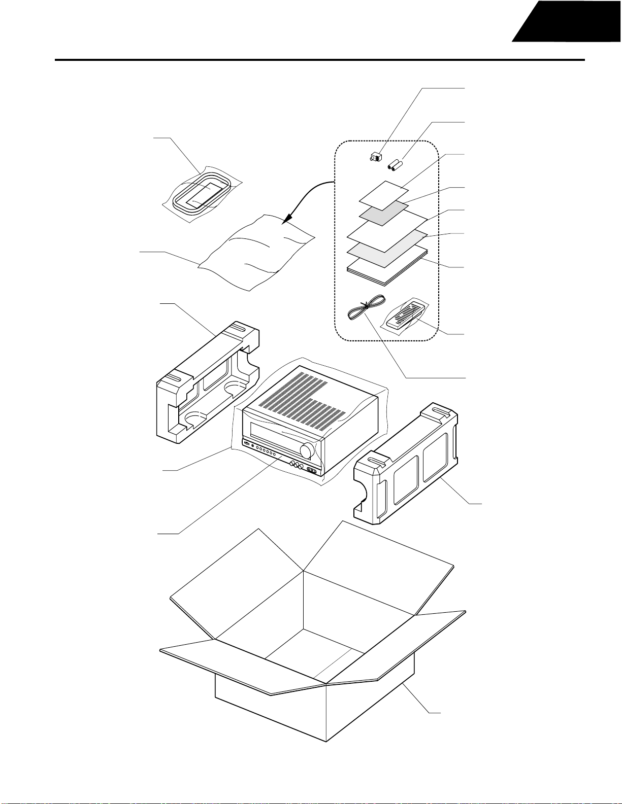
Harman Kardon
Dolby Digital Audio/Video Receiver
AVR78 & AVR85 PACKING EXPLODED VIEW
AM LOOP ANTENNA
#LA00055010
POLY BAG
FOAM PAD LEFT
#260J809012
AVR75/85
ANTENNA ADAPTER
#AA113
2 AAA BATTERIES
#1-01-102
WARRANTY CARD
#1119-047
SAFEGUARDS CARD
WARRANTY SERVICE SHEET
CAUTION FLY SHEET
#256J851010
OWNER'S MANUAL
AVR75 US - #294J851250
AVR75 EURO - #294J851310
AVR85 US - #288J851250
AVR85 EURO - #288J851310
REMOTE
AVR75 - #ZK294J0010
AVR85 - #ZK288J0010
POLYETHYLENE SHEET
AVR75 UNIT
or
AVR85 UNIT
FM ANTENNA
#ZA02000070
FOAM PAD RIGHT
#260J809022
CARTON
AVR75 - #294J801022
AVR85 - #288J801010
52
Page 55
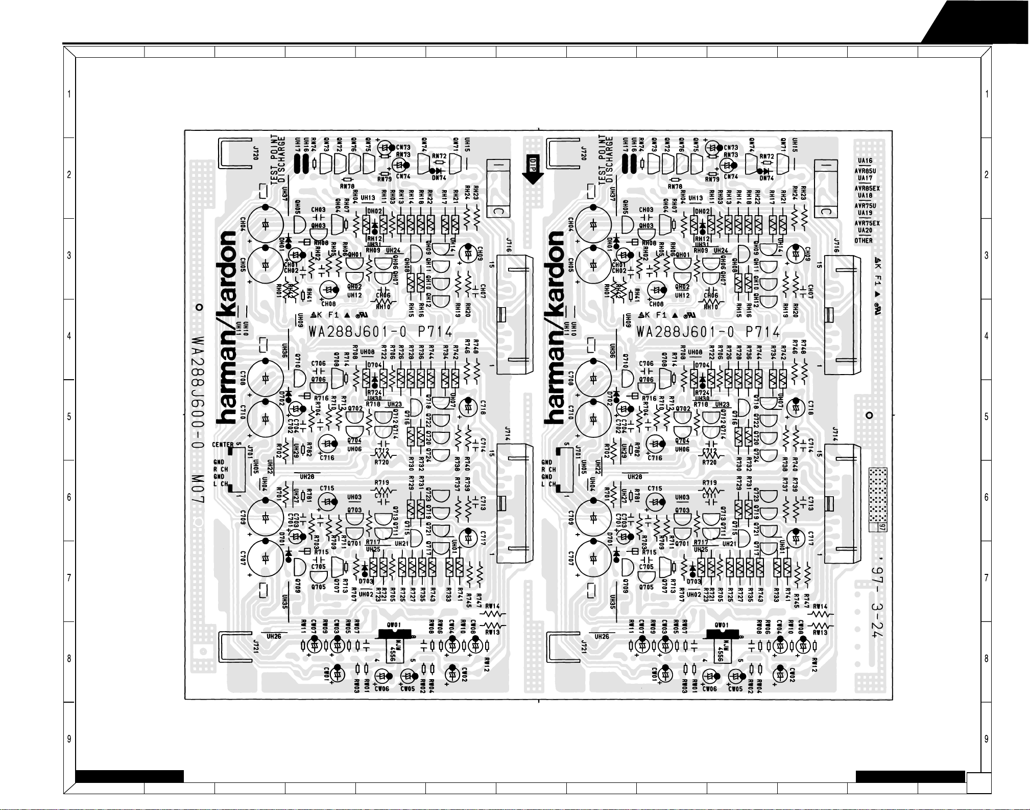
Harman Kardon
Dolby Digital Audio/Video Receiver
VOLTAGE AMP PCB - P714
EDCBA
HGF
I
J
LMK
AVR75/85
AVR75/85 PAGE 53-1of2
AB CDE
FGH
AVR75/85 PAGE 53-2of2
J
K
LMI
53
Page 56

Harman Kardon
Dolby Digital Audio/Video Receiver
AC3/DAC PCB - P604
EDCBA
HGF
I
J
LMK
AVR75/85
Component Side Shown Here
at 140% for added clarity
Solder Side Shown Here
at 140% for added clarity
AVR75/85 PAGE 54-1of2
ABCDE
FGH
AVR75/85 PAGE 54-2of2
J
K
LMI
54
Page 57
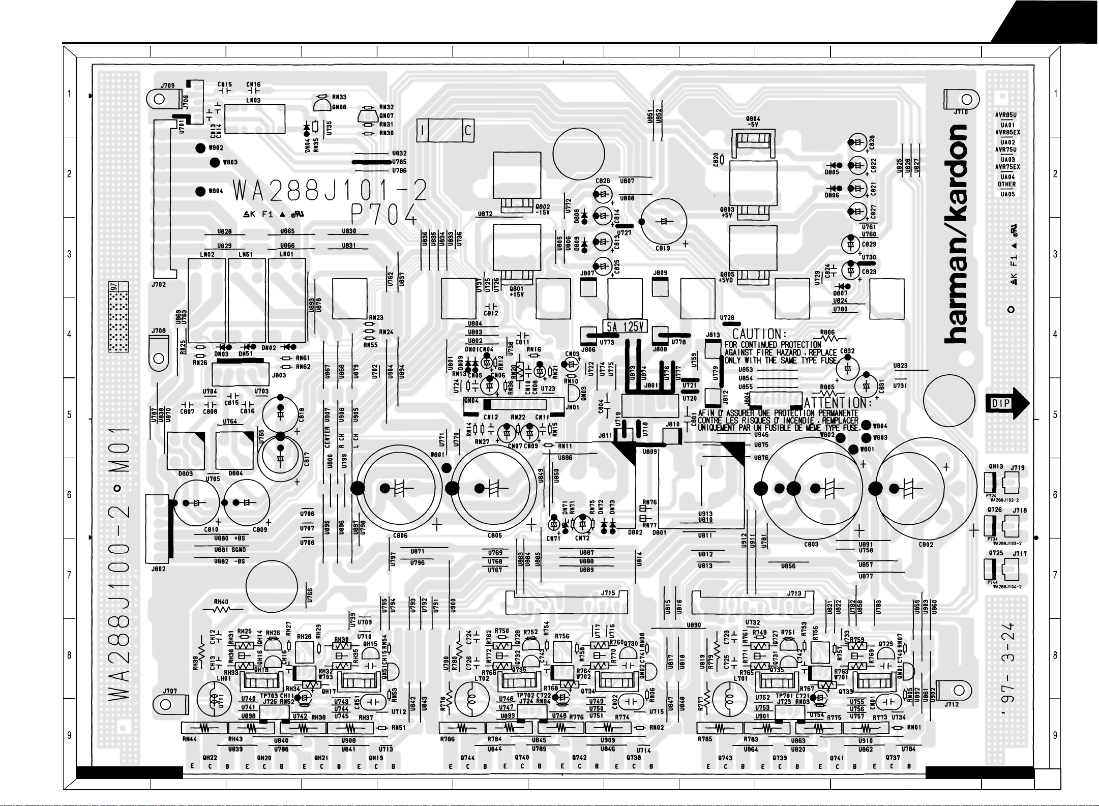
Harman Kardon
Dolby Digital Audio/Video Receiver
MAIN PCB -P704
EDCBA
HGF
I
J
LMK
AVR75/85
AVR75/85 PAGE 55-1of2
ABCDE
FGH
AVR75/85 PAGE 55-2of2
J
K
LMI
55
Page 58

Harman Kardon
Dolby Digital Audio/Video Receiver
AUDIO FUNCTION PCB - PS04, AUDIO/VIDEO PCB - PS54, ELECTRONIC VOLUME CONTROL PCB - PE04, AC-3 CROSSOVER PCB - PC04
EDCBA
HGF
I
J
AUDIO
FUNCTION
PCB - PS04
AUDIO/VIDEO
PCB - PS54
AVR75/85
LMK
AC-3 CROSSOVER
AC-3 CROSSOVER
PCB - PC04
PCB - PC04
AVR75/85 PAGE 56-1of2
ABCDE
ELECTRONIC VOLUME CONTROL PCB - PE04
FGH
AVR75/85 PAGE 56-2of2
J
K
LMI
56
Page 59
Harman Kardon
Dolby Digital Audio/Video Receiver
AVR75/85 PAGE 57-1of2
SPEAKER TERMINAL PCB - P754, VIDEO SELECTOR PCB - PL04, CONNECT PCB - PY04
EDCBA
HGF
I
J
AVR75/85
LMK
CONNECT PCB - PY04
SPEAKER TERMINAL
PCB - P754
ABCDE
FGH
VIDEO SELECTOR
PCB - PL04
J
AVR75/85 PAGE 57-2of2
K
LMI
57
Page 60

Harman Kardon
Dolby Digital Audio/Video Receiver
S-VIDEO
PCB - PL54
for 120V
AVR85 ONLY
S-VIDEO PCB - PL54, TUNER PCB - P104, STANDBY PCB - PB04, SURROUND AMP PCB - PP04, (FOR 120V)
EDCBA
HGF
I
J
AVR75/85
LMK
TUNER
PCB - P104
for 120V
STANDBY
PCB - PB04
for 120V
AVR75/85 PAGE 58-1of2
ABCDE
FGH
SURROUND
AMP
PCB - PP04
for 120V
AVR75/85 PAGE 58-2of2
J
K
LMI
58
Page 61

Harman Kardon
Dolby Digital Audio/Video Receiver
S-VIDEO
PCB - PL54
for 230V
AVR85 ONLY
S-VIDEO PCB - PL54, TUNER PCB - P104, STANDBY PCB - PB04, SURROUND AMP PCB - PP04 (FOR 230V)
EDCBA
HGF
I
J
AVR75/85
LMK
TUNER
PCB - P104
for 230V
STANDBY
PCB - PB04
for 230V
AVR75/85 PAGE 59-1of2
ABCDE
FGH
SURROUND
AMP
PCB - PP04
for 230V
AVR75/85 PAGE 59-2of2
J
K
LMI
59
Page 62

Harman Kardon
Dolby Digital Audio/Video Receiver
FRONT PCB - PU04, S-VIDEO PCB - PL54, MASTER VOLUME PCB - PU54, SPEAKER PROTECT PCB - PN54,
TONE CONTROL PCB - PF04, AUX IN PCB - PL94, POWER SWITCH PCB - PU94, HEADPHONE PCB - PW04
EDCBA
HGF
I
J
AVR75/85
LMK
FRONT PCB - PU04
SPEAKER
PROTECT
PCB - PN54
AUX IN
PCB - PL94
TONE
COLNTROL
PCB - PF04
MASTER VOLUME
PCB - PU54
POWER SWITCH
PCB - PU94
PCB - PW04
HEADPHONE
S-VIDEO PCB - PL54 for AVR75 ONLY
AVR75/85 PAGE 60-1of2
ABCDE
FGH
AVR75/85 PAGE 60-2of2
J
K
LMI
60
Page 63

Harman Kardon
Dolby Digital Audio/Video Receiver
QX60: LC74760
LSI
INTEGRATED CIRCUIT DIAGRAMS 1
DD1
V
30
SYNCDET
28
29
VCOOUT
VCOIN
27
FC
26 25
AMPOUT
AMPIN
24
LC74760
PDOUT
23
SS
V
22 21
SEPC
SYNCIN
20
19
CVCR
18
CVIN
AVR75/85
DD2
V
CVOUT
16
17
CS
SIN
SCLK
RST
SECAM
525/625
NTSC/PAL
3.58/4.43
V
DD1
V
SS
V
DD2
SYNCDET
VCOIN
VCOOUT
FC
AMPIN
AMPOUT
SYNCIN
SEPC
Serial
Parallel
Converter
Composite
Synchro-
nization
Signal
Control
AFC
Circuit
Sync
Separator
8-bit
Latch
and
Command
Decoder
Sync
Detector
Composite
Synchro-
nization
Signal
Separator
Control
HSYNCOUT VSYNCOUT
21
SS
V
Horizontal
Character
Size
Register
Horizontal
Size
Counter
3
IN1
OUT1
XTAL
XTAL
Vertical
Character
Register
Vertical
Counter
Timing Generator
4
HSYNCOUT
Size
Size
XTAL
5
XTAL
IN1
IN2
Horizontal
Display
Position
Register
Horizontal
Counter
Horizontal
Display
Position
Detection
Character
Control
Counter
XTAL
6
OUT2
XTAL
Dot
8
7
CS
VSYNCOUT
Vertical
Display
Position
Register
Vertical
Dot
Counter
Vertical
Display
Position
Detection
Line
Control
Counter
Synchronization
Signal Generator
XTAL
OUT1
9
10
SIN
SCLK
Flashing/
Reversal
Control
Register
Flashing/
Reversal
Control
Circuit
XTAL
IN2
13
1211
SECAM
525/625
Display
Control
Register
Character Output Control
Background Control
Video Output Control
CVCR
OUT2
NTSC/PAL
CVIN
14
3.58/4.43
CVOUT
15
RST
RAM
Write
Address
Counter
Decoder
Display
RAM
Decoder
Front
ROM
Shift
Register
QR01: LC8904Q
DIGITAL AUDIO I/F
38
DO
SRDT
CE/XLAT
CL/SCLK
42
39
LD/DOSY
DI/SWDT
41
37
40
2
SUB1
EMPHA
m -COM INTERFACE
CCB/SUB
5
33
32
SUB2
C BIT DETECT
20
SBSY
22
SFSY
PW
CD SUB CORD
21
DETECT
DIN1
44
SBCK
DIN2
23
30
35
36
34
BCLK
LRCK
DATAOUT
ERROR
DETECT
MUTE OUT
ERROR LOCK
DATA
DEMODULATION
PLXER
MULTI-
DOUT/V
DIN3
DIN4
45
46
47
CLKOUT 2
TIMING
CLKMD
CLK
8
1
9
29
28
10
XIN1
43
25
19
1412
DVDD AVDD DVDD DVDD DVDD
13
NC
16
AGND
6
24
31
XOUT
48
DGND DGND DGND DGND
26
27
TEST
TEST
CLKOUT 1
TEST
OSC
XTAL
GENERATOR
PLL
CIRCUIT
XMODE
VCO
RC1
R
RC2
VIN
3
7
11
4
18
15
17
61
Page 64
Harman Kardon
Dolby Digital Audio/Video Receiver
Q601: YSS243 AC-3 DECODER
SWIWCK
SDI0
SDI1
MUTE
AC3DATA
KARAOKE
VREF
/RAMCE
/RAMOE
/RAMWE
/RAMA0-14
/RAMD0-7
CRC
CPO
CRC
XI
XO
PLL
VIN
External RAM Interface
SDI (Serial Data Input) Interface
Input Buffer
Operating Clock (20MHz)
24bit DSP
SDO (Serial Data Output) Interface
SDO0
AC-3
SDO1
PCM
SDO2
INTEGRATED CIRCUIT DIAGRAMS 2
SDIBCK
SDO3
WCK
Control Signals
Control Registers
Control Signals
BCK
Microprocessor Interface
IPORT0-7
/CS
SCK
SI
SO
OPORT0-7
SDOWCK
SDOBCK
/SDOBCK
TESTI11
TESTI12
TESTI13
TESTI14
TESTI15
TESTI16
TESTI17
TESTI18
TESTI19
DVDD
AVDD
VREF
AVSS
DVSS
CPO
TESTBRK
TESTR1
TESTR2
DVDD
DVDD
TESTI20
TESTI21
TESTI22
TESTI23
TESTI24
TESTI25
TESTI26
TESTI27
TESTI28
VIN
XO
XI
TESTI10
TESTI9
TESTI8
TESTI7
TESTI6
TESTI5
TESTI4
TESTI3
TESTI2
TESTI1
TESTI0
121
119
124
123
37
38
RAMA8
RAMA9
122
39
RAMA11
120
40
41
/RAMOE
RAMA10
118
42
43
RAMD7
/RAMCE
126
128
125
127
1
2
3
4
5
6
7
8
9
10
11
12
13
14
15
16
17
18
19
20
21
22
23
24
25
26
27
28
29
30
31
32
33
34
35
36
TESTI29
TESTI30
RAMA13
/RAMAWE
TESTO0
TESTO1
116
117
44
45
RAMD6
RAMD5
TESTO2
TESTO3
115
114
46
47
RAMD4
RAMD3
TESTO4
113
48
DVSS
TESTO5
112
49
DVSS
TESTO6
TESTO7
111
110
50
51
RAMD1
RAMD2
TESTO8
TESTO9
109
108
52
53
RAMA0
RAMD0
TESTO10
TESTO11
106
107
54
55
RAMA1
RAMA2
TESTO12
TESTO13
105
104
56
57
RAMA3
RAMA4
TESTO14
OPORT0
103
102
58
59
RAMA5
RAMA6
OPORT1
OPORT2
101
100
60
61
RAMA7
RAMA12
OPORT3
OPORT4
99
98
62
63
IPORT0
RAMA14
OPORT5
97
96
95
94
93
92
91
90
89
88
87
86
85
84
83
82
81
80
79
78
77
76
75
74
73
72
71
70
69
68
67
66
65
64
IPORT1
AVR75/85
OPORT6
OPORT7
DVSS
DVSS
SDIWCK
SDIBCK
SDI0
SDI1
SCK
SI
SO
/CS
/IC
KARAOKE
MUTE
CRC
AC3DATA
SDOWCK
SDOBCK
/SDOBCK
SDO0
SDO1
SDO2
SDO3
DVDD
DVDD
IPORT7
IPORT6
IPORT5
IPORT4
IPORT3
IPORT2
Name
I/O
No.
1 TEST11 I N.C.
2 TEST12 I N.C.
3 TEST13 I N.C.
4 TEST14 I N.C.
5 TEST15 I N.C.
6 TEST16 I N.C.
7 TEST17 I N.C.
8 TEST18 I N.C.
9 TEST19 I N.C.
10 DVDD - +5VD
11 AVDD - +5VD
12 VIN AI PLL input
13 VREF AI PLL input
14 AVSS - GND
15 DVSS - GND
16 XO O N.C.
17 XI I External clock input
18 CPO AO PLL output
19 TESTBRK I N.C.
20 TESTR1 I N.C.
21 TESTR2 I N.C.
22 DVDD - +5VD
23 DVDD - +5VD
24 TEST20 I N.C.
25 TEST21 I N.C.
26 TEST22 I N.C.
27 TEST23 I N.C.
28 TEST24 I N.C.
29 TEST25 I N.C.
30 TEST26 I N.C.
31 TEST27 I N.C.
32 TEST28 I N.C.
33 TEST29 I N.C.
34 TEST30 I N.C.
35 /RAMWE O SRAM /WE
36 RAMA13 O SRAM A13
37 RAMA8 O SRAM A8
38 RAMA9 O SRAM A9
39 RAMA11 O SRAM A11
40 /RAMOE O SRAM /OE
41 RAMA10 O SRAM A10
42 /RAMCE O SRAM /CE
43 RAMD7 I/O SRAM D7
44 RAMD6 I/O SRAM D6
45 RAMD5 I/O SRAM D5
46 RAMD4 I/O SRAM D4
47 RAMD3 I/O SRAM D3
48 DVSS - GND
49 DVSS - GND
50 RAMD2 I/O SRAM D2
51 RAMD1 I/O SRAM D1
52 RAMD0 I/O SRAM D0
53 RAMA0 O SRAM A0
54 RAMA1 O SRAM A1
55 RAMA2 O SRAM A2
56 RAMA3 O SRAM A3
57 RAMA4 O SRAM A4
58 RAMA5 O SRAM A5
59 RAMA6 O SRAM A6
60 RAMA7 O SRAM A7
61 RAMA12 O SRAM A12
62 RAMA14 O SRAM A14
63 IPORT0 I N.C.
64 IPORT1 I N.C.
Function
Name
I/O
No.
65 IPORT2 I N.C.
66 IPORT3 I N.C.
67 IPORT4 I N.C.
68 IPORT5 I N.C.
69 IPORT6 I N.C.
70 IPORT7 I N.C.
71 DVDD - +5VD
72 DVDD - +5VD
73 SDO3 O PCM MIX0, MIX1 output
74 SDO2 O PCM C, LFE output
75 SDO1 O PCM LS, RS output
76 SDO0 O PCM L, R output
77 /SDOBCK O N.C.
78 SDOBCK I SDO bit clock input
79 SDOWCK I SDO work clock input
80 AC3DATA O N.C.
81 CRC O N.C.
82 MUTE O Set to 1 if error data is detected when auto muting function triggered
83 KARAOKE O N.C.
84 /IC I Initial clear
85 /CS I m-com interface chip select input
86 SO O m-com interface data output
87 SI I m-com interface data input
88 SCK I m-com interface clock input
89 SDI1 I N.C.
90 SDI0 I AC-3 bit stream (or PCM) data input
91 SDIBCK I SDI bit clock input
92 SDIWCK I SDI work clock input
93 DVSS - GND
94 DVSS - GND
95 OPORT7 O N.C.
96 OPORT6 O N.C.
97 OPORT5 O N.C.
98 OPORT4 O N.C.
99 OPORT3 O N.C.
100 OPORT2 O N.C.
101 OPORT1 O N.C.
102 OPORT0 O N.C.
103 TESTO14 O N.C.
104 TESTO13 O N.C.
105 TESTO12 O N.C.
106 TESTO11 O N.C.
107 TESTO10 O N.C.
108 TESTO9 O N.C.
109 TESTO8 O N.C.
110 TESTO7 O N.C.
111 TESTO6 O N.C.
112 TESTO5 O N.C.
113 TESTO4 O N.C.
114 TESTO3 O N.C.
115 TESTO2 O N.C.
116 TESTO1 O N.C.
117 TESTO0 O N.C.
118 TESTI0 I N.C.
119 TESTI1 I N.C.
120 TESTI2 I N.C.
121 TESTI3 I N.C.
122 TESTI4 I N.C.
123 TESTI5 I N.C.
124 TESTI6 I N.C.
125 TESTI7 I N.C.
126 TESTI8 I N.C.
127 TESTI9 I N.C.
128 TESTI10 I N.C.
Function
62
Page 65
Harman Kardon
Dolby Digital Audio/Video Receiver
INTEGRATED CIRCUIT DIAGRAMS 3
Q651: SUB CPU (AC-3 DSP)
TMP87CH40F MICROPROCESSOR
PORT
PORT
No.
NAME
1 P76 O CAL RESET&CALIBRATE FOR ADC H:RESET&CAL,L:NORMAL
2 P77 O RSTO RESET OUT FOR DAI&DEMODURATOR L:RESET,H:NORMAL
3 P00 O CS SPI CHIP SELECT FOR YSS243
4 P01 O CRS SPI CPU I/F RESET FOR YSS241
5 P02 O FS0 Fs SET FOR YSS241
6 P03 O FS1 Fs SET FOR YSS241
7 P04 O MUTE-S DAC MUTE CONT. OUT L:MUTE H:NORMAL
8 P05 O EMP-1 DAC EMP.CONT.1
9 P06 O EMP-2 DAC EMP.CONT.2
10 P07 O YRST RESET OUTPUT FOR YSS241&243L:RESET H:NORMAL
11 P10/INT0 N.C.
12 P11/INT1 N.C.
13 P12/INT2 I (DEBUG) FIXED+5V
14 P13/DVO N.C.
15 P14/PPG N.C.
16 P15/TC2 N.C.
17 P16 N.C.
18 P17 N.C.
19 P20/INT5 I/O IFREQ REQUEST SIGNAL FOR MAIN CPU I/F
20 TEST GND
21 P21/XTIN N.C.
22 P22/XTO N.C.
23 RESET I RSTI RESET INPUT FROM MAIN CPU L:RESET
24 XIN I XIN FOR CPU OSC
25 XOUT O XOUT FOR CPU OSC
26 VSS GND
27 P30
28 P31 N.C.
29 P32 N.C.
30 P33 N.C.
31 P34 N.C.
32 P35 N.C.
33 P36 N.C.
34 P37 N.C.
35 P40 O CE0 CHIP ENABLE OUT FOR I/F TO DAI(LC8904Q)
36 P41 I/O IFACK ACKNOWLEDGE SIGNAL FOR MAIN CPU I/F
37 P42/SCK1 O CL/SCK SPI CLOCK OUT TO DAI(LC8904Q)&YSS241,243
38 P43/SI1 I DO/SO SPI DATA IN FROM DAI&DSP(YSS243)
39 P44/SO1 O DI/SI SPI DATA OUT TO DAI&DSP(YSS241&243)
40 P45/SCK2 O IFCLK I/F CLOCK OUT TO MAIN CPU
41 P46/SI2 I IFDATAI I/F DATA IN FROM MAIN CPU
42 P47/SO2 O IFDATAO I/F DATA OUT TO MAIN CPU
43 P50/INT3 I C1F0 DEMODURATOR ERROR INPUT(FOR DEBUG USE ONLY)
44 P51/INT4 I ERROR DAI ERROR INPUT L:Error H:OK
45 P52/PDO N.C.
46 P53 N.C.
47 P54 N.C.
48 VASS GND
49 VAREF GND
50 P60/AIN0 O DEBO CHIP ENABLE OUT FOR DEBUG USE ONLY
51 P61/AIN1 N.C.
52 P62/AIN2 I YMUTE YSS241 ERROR MUTE INPUT(H:MUTEON,L:MUTEOFF)
53 P63/AIN3 N.C.
54 P64/AIN4 N.C.
55 P65/AIN5 N.C.
56 P66/AIN6 N.C.
57 P67/AIN7 N.C.
58 VDD +5V
59 P70 O OSCON PM4007A OSC CONTROL H:ONL:STOP
60 P71 O DSEL DATA SELECT(YSS243or241)H:241L:243
61 P72 O LFE-ATT LFEATT.CONT.H0dB L:-10dB,OFF
62 P73 O A/D ADC/DAI SELECT H:DAI L:ADC
63 P74 O RF/OTH RF/OTHER SELECT H:RF L:THER
64 P75 O MUTE-1 MUTE CONTROLLED BY SUB CPU H:NORMAL L:MUTE
I/O
SIGNAL
NAME
FUNCTION
NOTES
DATA
BCK
TEST1
TEST2
QD01, QD31, QD51: TDA1305T
D/A CONVERTER
PINNING
PIN
SYMBOL
V 1 analog supply voltage
DDA
V 2 analog ground
SSA
TEST1 3 test input; pin should be connected
BCK 4 bit clock input
WS 5 word select input
DATA 6 data input
CLKS1 7 clock selection 1 input
CLKS2 8 clock selection 2 input
V 9 digital ground
SSD
V 10 digital supply voltage
DDD
TEST2 11 test input; pin should be connected
SYSCLKI 12 system clock input
n.c. 13 not connected (this pin should be left
n.c. 14 not connected (this pin should be left
V 15 digital ground
SSD
SYSCLKO 16 system clock output
DEEM1 17 de-emphasis on/off; f 32 kHz,
DEEM2 18
MUSB 19 mute input (active LOW)
DSMB 20 double-speed mode input
ATSB 21 12 dB attenuation input
VOL 22 left channel output
FILTCL 23 capacitor for left channel 1st order
FILTCR 24 capacitor for right channel 1st order
VOR 25 right channel output
V 26 internal reference voltage for output
ref
V 27 operational amplifier ground
SSO
V 28 operational amplifier supply voltage
DDO
DSMB AYSB DEEM1 DEEM2 MUSB
21
20
6
SERIAL
5
WS
DATA
INPUT
4
3
11
FIR FILTER STAGE1
FIR FILTER STAGE2
LINEAR INTERPOLATOR
6 x OVERSAMPLING
(SAMPLE-AND-HOLD)
2nd ORDER
NOISE SHAPER
DATA
ENCODER
DESCRIPTION
to ground (internal pull-down
resistor)
to ground (internal pull-down
resistor)
open-circuit)
open-circuit)
V
DD
18
s
s
s
s
6 x OVERSAMPLING
(SAMPLE-AND-HOLD)
2nd ORDER
NOISE SHAPER
DATA
ENCODER
DEEM
DEEM
19
44 kHz and 48 kHz
de-emphasis on/off; f 32 kHz,
44 kHz and 48 kHz
(active LOW)
(active LOW)
filter function should be connected
between pins 22 and 23
filter function should be connected
between pins 25 and 24
channels (0.5 )
17
FIR FILTER
1f
2f
8f
16f
AVR75/85
CLKS1 CLKS2
7
8
12
TIMING
16
14
13
10
9
SYSCLKI
SYSCLKO
n.c.
n.c.
V
DDD
V
SSD
C
C
EXT1
1nF
EXT3
1Fm
FILTCL
VOL
V
23
R
CONV1
2kW 2kW
22
26
ref
16 (4-bit)
CALIBRATED
CURRENT
SOURCES
_
LEFT
OUTPUT
OP1 OP1
+
SWITCHES
27 28
V
SSO
16 (4-bit)
CALIBRATED
CURRENT
V
SINKS
DDO
REFERENCE
SOURCE
15
V
SSD
16 (4-bit)
CALIBRATED
CURRENT
SOURCES
RIGHT
OUTPUT
SWITCHES
16 (4-bit)
CALIBRATED
CURRENT
SINKS
12
V
DDAVSSA
R
CONV2
_
+
TDA1305T
24
25
FILTCR
VOR
C
EXT2
1nF
63
Page 66
Harman Kardon
Dolby Digital Audio/Video Receiver
Q602: YSS241 PRO LOGIC DECODER
/CRS
I2CCL
I2CDA
/I2CSEL
MODE1,0
I2SWS
I2SCL
I2SSDI
I2SSDO
LRCK
64FS
ADD
ADSEL
FS1,0
/EMP
DALR
DACS1
DACS2
DAWC
DABC
No Name I/O Function
1 ADD I A/D CONVERTER SOUND DATA INPUT
2 64FS O ADC BIT CLOCK OUTPUT
3 LRCK O ADC L/R CLOCK OUTPUT
4 256FS O ADC MASTER CLOCK OUTPUT
5 VSS - GND
6 XI I EXTERNAL CLOCK OUTPUT
7 XO O N.C.
8 /I2CSEL I SELECTS CPU INTERFACE (“H”: SERIAL
9 /IC I INITIAL CLEAR INPUT
10 VDD - +5VD
11 I2SSDO O INVALID
12 I2SSDI I DIR2 SOUND DATA INPUT
13 I2SWS I DIR2 L/R CLOCK INPUT
14 I2SCL I GND
15 TEST1 I N.C.
16 TEST0 I N.C.
17 MODE1 I N.C.
18 MODE0 I N.C.
19 DAMODE I SELECTS AUDIO DATA OUTPUT FORMAT
20 TEST2 I N.C.
21 TEST3 I N.C.
22 TEST4 I N.C.
23 TEST5 I N.C.
24 TEST6 I N.C.
25 TEST7 I N.C.
26 TEST8 I N.C
27 TEST9 I N.C.
28 TEST10 I N.C.
29 TEST11 I N.C.
30 TEST12 I N.C.
31 TEST13 I N.C.
32 TEST14 I N.C.
I2C
Interface
MSP3410
Interface
/IC
3-WIRE TYPE, “L”: 12C BUS TYPE)
Microprocessor
INTEGRATED CIRCUIT DIAGRAMS 4
Interface
DIR2
ADC
Interface
DAC
Interface
DAMODE
OVFL
MUTE
Main
DSP
OVFR
Delay RAM
Sub
DSP
Timing
Generator
XI
XO
DAMC
256FS
No Name I/O Function
33 TEST15 I N.C.
34 TEST16 I N.C.
35 DAWC O DAC L/R CLOCK OUTPUT
36 DABC O DAC BIT CLOCK OUTPUT
37 DAMC O DAC MASTER CLOCK
38 VSS - GND
39 TEST17 I N.C.
40 DACS1 O DAC AUDIO DATAOUTPUT
41 DALR O DAC AUDIO DATAOUTPUT
42 DAS2 O DAC AUDIO DATA OUTPUT
43 VDD - +5V
44 TEST18 O N.C.
45 TEST19 O N.C.
46 TEST20 I N.C.
47 TEST21 O N.C.
48 TEST22 I N.C.
49 TEST23 I N.C.
50 TEST24 I N.C.
51 TEST25 I N.C.
52 I2CDA I/OD CPU/I2C BUS INTERFACE SERIAL DATAINPUT
53 I2CCL I CPU/I2C BUS INTERFACE BIT CLOCK INPUT
54 TEST26 O N.C.
55 /CRS I SERIAL 3-WIRE TYPE (/I2CSEL= “H”) :CPU INTERFACE RESET INPUT
56 MUTE O SYSTEM MUTE DETECTION
57 OVFL O N.C.
58 OVFR O N.C.
59 TEST27 O N.C.
60 TEST28 O N.C.
61 ADSEL I AUDIO DATA INPUT SWITCH (“H” :ADD INPUT, “L” :I2SSDI INPUT)
62 FS1 I SAMPLING FREQUENCY SWITCHER (VALID ONLY WHEN ADSEL= “L”)
63 FS0 I SAMPLING FREQUENCY SWITCHER (VALID ONLY WHEN ADSEL= “L”)
64 /EMP I DE-EMPHASIS PROCESSING (“L” :ON)
ADD
64FS
LRCK
256FS
VSS
/I2CSEL
VDD
I2SSDO
I2SSDI
I2SWS
I2SCL
TEST1
TEST0
MODE1
MODE0
DAMODE
1
2
3
4
5
XI
6
XO
7
8
/IC
9
10
11
12
13
14
15
16
17
18
19
/EMP
64
20
TEST2
FS0
63
21
TEST3
FS1
62
22
TEST4
ADSEL
61
23
TEST5
TEST28
TEST27
60
59
24
25
TEST6
TEST7
OVFR
58
26
TEST8
OVFL
57
27
TEST9
MUTE
/CRS
56
55
28
TEST10
29
TEST11
TEST26
I2CCL
54
53
30
31
TEST12
TEST13
I2CDA
52
51
50
49
48
47
46
45
44
43
42
41
40
39
38
37
36
35
34
33
32
TEST14
AVR75/85
TEST25
TEST24
TEST23
TEST22
TEST21
TEST20
TEST19
TEST18
VDD
DAS2
DALR
DACS1
TEST17
VSS
DAMC
DABC
DAWC
TEST16
TEST15
QK01: AK5340 A/D CONVERTER
TST3
21
LP Filter
DAC
LP Filter
DAC
VREF
VREFIN
AINL
AINL
AINR
AINR
TST1
26
3
8
TST2
11
Voltage
Reference
1
2
>
>
45
VA
AGND
TST4
CLK20SCLK
22
15
Serial Output
>
Decimation
Filter
Decimation
>
Filter
Controller
PD
24
10
VDB
9
SEL18
L/R
14
Interface
Calibration
SRAM
18
VDP
FSYNC
17
>
DGND
16
SDATA
>
12
CMODE
13
SMODE
19
64
Page 67
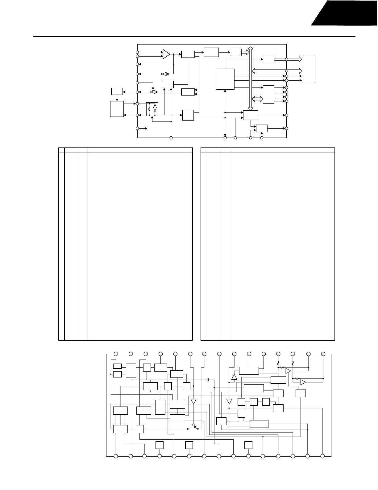
Harman Kardon
Dolby Digital Audio/Video Receiver
AVR75/85
INTEGRATED CIRCUIT DIAGRAMS 5
QM09: PM4007A
QPSK Input
RF DEMODULATOR
VCXO
18.432 MHz
Name
I/O
At "H" during normal operation At "L" during standby
No.
1 GND - GND
2 VDD - +5VD
3 RESET I System Reset At "L" reset
4 OSCON I Oscillator Control
5 DATA I TEST
6 MCK I TEST
7 MLTB I TEST
8 IDST O TEST
9 IDCK O TEST
10 IDO O TEST
11 TM0 I TEST
12 ECCK O TEST
13 DEN O TEST
14 DRY O TEST
15 MSYC O TEST
16 TM1 I TEST
17 A0 O RAM A0
18 A1 O RAM A1
19 A2 O RAM A2
20 A3 O RAM A3
21 A4 O RAM A4
22 A5 O RAM A5
23 TM2 I TEST
24 TM3 I TEST
25 XOUT O TEST
26 XIN I TEST
27 XENT I TEST
28 GND - GND
29 VDD - +5VD
30 A6 O RAM A6
31 A7 O RAM A7
32 GND - GND
33 VDD - +5VD
34 A12 O RAM A12
35 A14 O RAM A14
36 WEB O RAM WEB
37 A13 O RAM A13
38 A8 O RAM A8
39 A9 O RAM A9
40 GND - GND
41 A11 O RAM A11
42 OEB O RAM OE
43 A10 O RAM A10
44 DB7 B RAM D7
45 DB6 B RAM D6
46 DB5 B RAM D5
47 DB4 B RAM D4
48 DB3 B RAM D3
49 DB2 B RAM D2
50 DB1 B RAM D1
SYNC
CPIN
CMIN
Demoduration
DetectionSafeguard
DOUT
DOUTB
PDDIS
PDO
LPF
46.08 MHz
Oscillator
46.08 MHz
Phase
Comparator
9 KHz
VI
VO
1/2048
Divider
1/2
RESET
Timing
9.216 KHz
S/P
Address
Error
Correction
DAI
Control
SW
A(14:0)
DB(7:0)
OEB
WEB
C2F1
C2F0
C1F1
C1F0
MUTO
DAOUT
SRAM
32Kx8
Serial data stream output
C9M
MUTI
DAIN
Function
Sets to "H" when MUTI = H or the AC-3 period cannot be received.
Function
OSCON
Name
I/O
O TEST
No.
51 DB0 B RAM D0
52 VDD - +5VD
53 GND - GND
54 TI1 I TEST
55 VIN I VCXO input
56 VOUT O VCXO output
57 TI2 I TEST
58 TI3 I TEST
59 TLDB I TEST
60 TCK I TEST
61 TRP O TEST
62 TDO O TEST
63 PDO O Phase comparator output (3-state)
64 TI4 I TEST
65 PDDIS I Control input for PDO out At "L" Output ON
66 MUTO O Muting output. Mutes at "H."
67 TI5 I TEST
68 VLDY
69 DASYO O TEST
70 DAOUT O Digital OUT (serial data stream output)
71 DAIN I Digital external input: Sets to DAOUT when DASEL is at "H"
72 DASEL I Selects digital OUT
73 TI8 I TEST
74 C2F1 O N.C.
75 C2F0 O N.C.
76 C1F1 O N.C.
77 C1F0 O Displays C1 correction error status. Outputs error count at C1.
78 MUTI I Muting input. Mutes at "H."
79 VDD - +5VD
80 GND - GND
81 AVDD - +5VD
82 CPIN I Analog converter inverted input
83 CMIN I Analog converter inverted input
84 AGND - GND
85 TM4 I TEST
86 VDD - +5VD
87 DIN I TEST
88 DOUT O Analog converter inverted input
89 DOUTB O Analog converter inverted reverse output
90 C9M O N.C.
91 GND - GND
92 WINGT O TEST
93 SYST0 O TEST
94 SYST1 O TEST
95 ADST0 O TEST
96 ADST1 O TEST
97 TM5 I TEST
98 BUNRI I TEST
99 AGND - GND
100 AVDD - +5VD
Q201: LA1836
FM/AM IF, MPX
30
ALC
BUFF
1
LEVEL
DET
FM IF
OSC
25
2829
AM
AM
RF AMP
MIX
26
27
AM
AGC
S-CURVE
FM
DET
S METER
AM/FM
IF
BUFF
AM
IF
COMP
TUNING
DRIVE
AM
DET
AM
FM
23
24
22
DECODER
ANTI SIROIE
FF FF FF
VCO
AM/FM
SW
REG GND
5
3
2
4
6
7
89
21
STEREO
VCC
10
DRIVE
PHASE DET
20
STEREO
PILOT
11 12
SW
TRIG
DET
1819
16
17
MUTE
13
15
14
65
Page 68
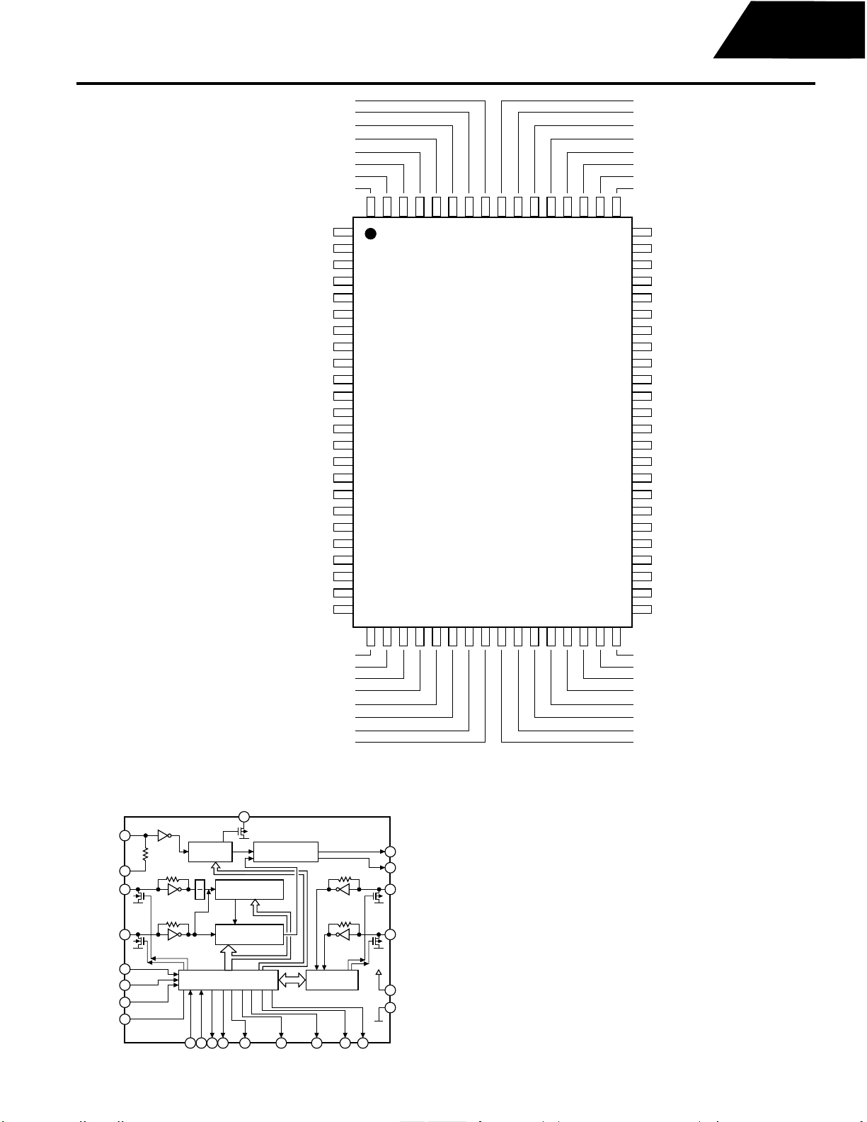
Harman Kardon
Dolby Digital Audio/Video Receiver
AVR75/85
INTEGRATED CIRCUIT DIAGRAMS 6
QU01: TMP87CP71F
MICROPROCESSOR
ENC (A) IN PULS ENC.
ENC (B) IN PULS ENC.
RC-5 OUT
RDS START BIN IN
MULTI ROOM RC DATA DET.
DS CLOCK IN
CE2 (OSD) OUT
AUTO MODE L:STEREO (DSP)
OSD SYNC. DET. IN
POWER DET. (L:STAND-BY)
N.C.
SD IN
PLL DATA IN
RESET IN
8 MHz
8 MHz
GND
POWER DOWN IN
RC-5 IN
REQ I/O
m
SUB -COM SCK IN
m
SUB -COM DATA IN
m
SUB -COM DATA OUT
CLK-1 OUT
m
SUB -COM ACK I/O
DATA-0 (OSD) OUT
KEY IN CIN4
KEY IN CIN3
KEY IN CIN2
KEY IN CIN1
KEY IN CIN0
SIG. STR. IN
P10/INTO
INP11/INT1
INP12/INT2
P13
P14
P15
P16
P17
TEST
P21
P22
RESET
XIN
XOUT
VSS
P20
P30/INT3
P31
P32
P33
P34
P35
P36
P37
78
79
80
1
2
3
4
5
6
7
8
9
10
11
12
13
14
15
16
17
18
19
20
21
22
23
24
25 262728 29
K5 KEY IN (K5)
K4 KEY IN (K4)
K3 KEY IN (K3)
K2 KEY IN (K2)
K1 KEY IN (K1)
K0 KEY IN (K0)
Vkk -30V
Sa SEGMENT a
76
77
74
75
73
30
31
32
72 71
33
34 35
70
69 686766
36
37
65
40
39
38
Sb SEG. b
64
Sc SEG. c
63
Sd SEG. d
62
Se SEG. e
61
Sf SEG. f
60
Sg SEG. g
59
Sh SEG. h
58
Si SEG. i
57
Sj SEG. j
56
Sk SEG. k
55
Sl SEG. l
54
Sm SEG. m
53
Sn SEG. n
52
So SEG. o
51
Sp SEG. p
50
G1 DIGIT D1
49
G2 DIGIT D2
48
G3 DIGIT D3
47
G4 DIGIT D4
46
G5 DIGIT D5
45
G6 DIGIT D6
44
G7 DIGIT D7
43
G8 DIGIT D8
42
G9 DIGIT D9
41
CE4 (TC9174 ENABLE)
RDS DATA IN
PORT EXP.1 (TC9173P) DATA IN
CLK-0 OUT
DATA-0 OUT
POWER ON/OFF OUT (H:ON)
CE3 OUT (TC9173P)
VOL.1-CLOCK OUT (FRONT)
Q501: LC7218 PPL
XIN
1
24
XOUT
FM IN
19
AM IN
18
CE
2
DI
3
CL
4
DO
5
REFERENCE
DIVIDER
1
2
89
7
6
SWALLOW COUNTER
I/16, I/17 4bit
12bit PROGRAMMABLE
DEVICER
SHIFT REGISTER
LATCH
10
11 12
SVC
PHASE DETECTOR
CHARGE PUMP
P00
P01
P02
P03
P04
P05
P06
P07
UNIVERSAL
COUNTER
13
14 17
PD1
PD2
HC TR
LC TR
G10 DIGIT D10
G11 DIGIT D11
G12 DIGIT D12
VOL. 3-CLOCK OUT (CEN./SUB-W.)
VOL. 2-CLOCK OUT (SURR.)
IR SENSOR SW CONT.
TAPE MONITOR LED OUT (H:ON)
VDD +5.5V
21
22
16
15
V
DD
20
Vss
23
66
Page 69
Harman Kardon
Dolby Digital Audio/Video Receiver
AVR75/85
INTEGRATED CIRCUIT DIAGRAMS 7
QS57 - LC78212 ANALOG SWITCH
L1
L2
L3
LCOM1
L4
L5
L6
LCOM2
L7
L8 L8
LCOM3
VDD
VSS
VEE
RES
S
Level Shift
Latch
Shift Register
Control
R1
R2
R3
RCOM1
R4
R5
R6
RCOM2
R7
R8 R8
RCOM3
DI
CL
CE
Q512 - LC78213 ANALOG SWITCH
L1
L2
LCOM1
L3
L4
LCOM2
L5
L6
LCOM3
L7
LCOM4
VDD
VSS
VEE
RES
Level Shift
Latch
Shift Register
S
Control
R1
R2
RCOM1
R3
R4
RCOM2
R5
R6
RCOM3
R7
RCOM4
DI
CL
CE
L1
L2
L3
L4
LCOM1
L5
L6
LCOM2
L7
LCOM3
VDD
VSS
VEE
RES
Q511, Q556 - LC78211 ANALOG SWITCH
Level Shift
Latch
Shift Register
S
Control
QY12 - TC9215 ANALOG SWITCH
161
OFF
S
S
C
S
S
V
10
11
12
20
21
SS
SW
SW
1
2
SW
SW
SW
SW
152
4
143
4
134
125
116
3
107
3
98
QE04, 05, 06, QG04-07, QG57 - TC9213P
ELECTRIC VOLUME CONTROL
R1
R2
R3
R4
RCOM1
R5
R6
RCOM2
R7
RCOM3
DI
CL
CE
V
DDGND
S
40
S
41
S
42
S
34
S
32
S
31
S
30
+5, +15V REGULATORS
Q801 - NJM7815
Q803 - NJM7805
1
INPUT
2
COMMON
3
OUTPUT
-5, -15V REGULATORS
Q802 - NJM7915
Q804 - NJM7905
1
COMMON
2
INPUT
3
OUTPUT
33
1122
V
OUT1
A-GND
OUT2
Left Channel
GND
SS
IN1
IN2
CK
1
2
3
4
5
6
7
8
(TOP VIEW)
16
15
14
13
12
TC9213P
11
10
9
V
DD
OUT1
IN1
A-GND
OUT2
IN2
STB
DATA
Right Channel
67
Page 70
Harman Kardon
Dolby Digital Audio/Video Receiver
Q652 - 74HC541
3-STATE BUFFER/
LINE DRIVER
DE1
A1
A2
A3
A4
A5
A6
A7
A8
GND
1
2
3
4
5
6
7
8
9
10
20
V
CC
19
DE2
18
Y1
17
Y2
16
Y3
15
Y4
14
Y5
13
Y6
12
Y7
11
Y8
INTEGRATED CIRCUIT DIAGRAMS 8
QC11 - NJU7311L
ANALOG SWITCH
V
EE
L1
L2
L-COM1
L3
L4
L-COM2
L5
L6
L-COM3
L7
L-COM4
ST
V
SS
V
DD
R1
R2
R-COM1
R3
R4
R-COM2
R5
R6
R-COM3
R7
R-COM4
DATA
CK
QM10 - 8X32 SRAM
A14
A12
I/O 0
I/O 1
I/O 2
GND
A7
A6
A5
A4
A3
A2
A1
A0
11
22
33
44
55
66
77
88
99
1010
1111
1212
1313
1414
AVR75/85
2828
VCC
2727
WE
2626
A13
2525
A8
2424
A9
2323
A11
2222
OE
2121
A10
2020
CE
1919
I/O 7
1818
I/O 6
1717
I/O 5
1616
I/O 4
1515
I/O 3
QF01 - NJM2058
QUAD OP-AMP
OUTPUT 1
-INPUT 1
+INPUT 1
+INPUT 2
-INPUT 2
OUTPUT 2
+V
1
2
3
4
5
6
7
14
13
12
11
10
9
8
OUTPUT 4
-INPUT 4
+INPUT 4
-V
+INPUT 3
-INPUT 3
OUTPUT 3
Q604 - 74HC157A
QUAD 2-INPUT MULTIPLEXER
S
1I
1I
1Y
2I
2I
2Y
GND
1
2
0
3
1
4
5
0
1
6
7
8
16
15
14
13
12
11
10
V
CC
E
4I
0
4I
1
4Y
3I
0
3I
1
3Y
9
QR02 - TC74CH00AP
QUAD 2-INPUT NAND GATE
1A
1B
1Y
2A
2B
2Y
GND
1
2
3
4
5
6
7
14
13
12
11
10
9
8
V
4B
4A
4Y
3B
3A
3Y
Q607, 608 - 74HC164E
8-BIT SERIAL-IN/PARALLEL-OUT
SHIFT REGISTER
D
SA
D
SB
Q
Q
Q
Q
GND
0
1
2
3
V
Q
Q
Q
Q
MR
CP
CC
7
6
5
4
CC
QT04 - 74LS132
QUAD 2-INPUT NAND
SCHMITT TRIGGER
1
A
0
2
B
0
3
O
0
4
A
1
5
B
1
6
0
1
7
GND
Q605 - 74HC74
DUAL D-TYPE FLIP-FLOP
1D
1Q
1Q
11
D
22
33
44
D
55
66
77
1R
1CP
1S
GND
14
V
CC
13
A
2
12
B
2
11
0
2
10
A
3
9
B
3
8
0
3
1414
V
CC
2R
1313
1212
1111
1010
D
2D
2CP
2S
D
99
2Q
88
2Q
68
Page 71
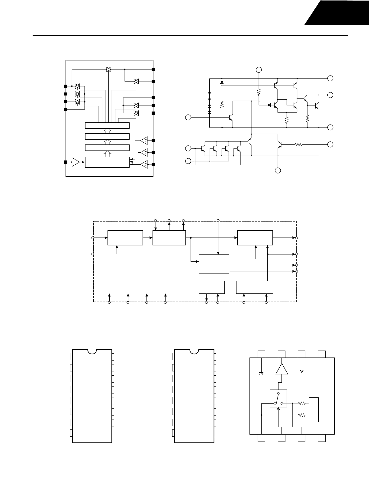
Harman Kardon
Dolby Digital Audio/Video Receiver
QL01, QL51, QL52 - LC7824
ANALOG SWITCH
SW7
L1
L2
L3
LCOM1
S
SW1
SW2
SW3
Level Shift
Shift Register
Latch
Control
INTEGRATED CIRCUIT DIAGRAMS 9
QN84 - TA7317P OVERLOAD PROTECTOR
COM3
SW6
IN6
COM2
SW5
IN5
SW4
IN4
CE
DI
CL
1
2
3
AVR75/85
8
9
6
4
7
5
DATA IN
CLOCK IN
QY10 - TC9173
PORT EXPANDER
GND
I/O-1
I/O-2
I/O-3
I/O-4
I/O-5
I/O-6
11
22
33
44
55
66
77
Q902 - LC7073 RDS ERROR MODULATOR
CD.S.CONTROL
SYNCHRONISM
OSCILLATOR SYSTEM CONTROL
OSC2
SERIAL/PARALLEL
CONVERTER
DD
ERROR
CORR. SEL
ERROR CHECK
CORRECTION
QY11 - TC9174P
PORT EXPANDER
16 16
V
DD
15 15
STB
14 14
CK
13 13
SI
12 12
SO
11 11
I/O-10
10 10
I/O-9
GND
OP-1
OP-2
OP-3
OP-4
OP-5
OP-6
CHECK
OSC1VSS3VSS2VSS1V
V
DD
STB
CK
SI
SO
OP-10
OP-9
SERIAL/PARALLEL
CONVERTER
SYNCHRONISM
A, B, C, C', D
RES CL.ED.SEL
DATA OUT
CLOCK OUT
DATA START
RECEIVE
QL04, QL05 - NJM2233D
VIDEO AMP
GND V out V+ NC
8
BUFFER
7
6
BIAS
5
I/O-7
I/O-8
88
99
OP-7
OP-8
1
Vin1 CTL Vin2 NC
2
3
4
69
Page 72
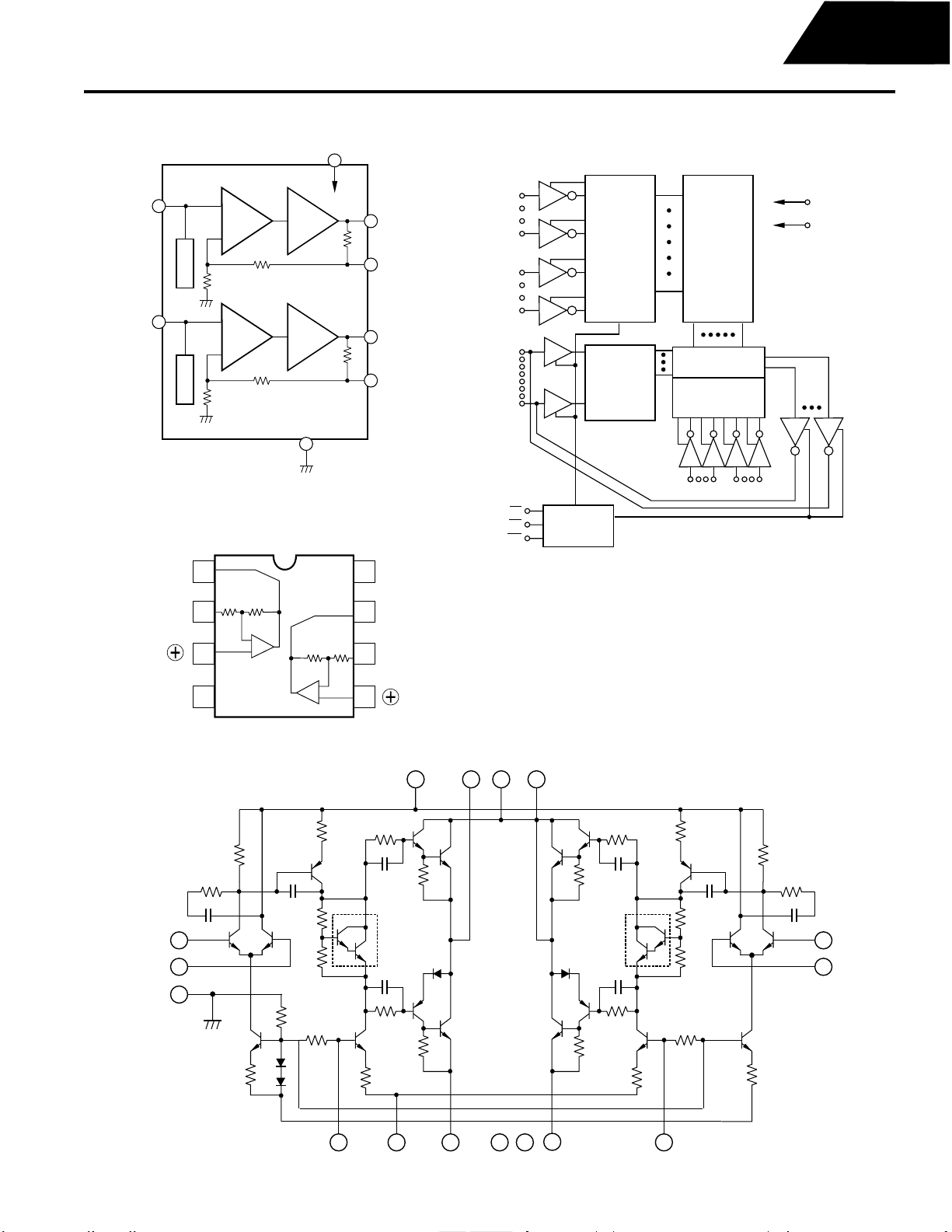
Harman Kardon
Dolby Digital Audio/Video Receiver
AVR75/85
INTEGRATED CIRCUIT DIAGRAMS 10
QX63 - NJM2267D VIDEO AMP
V+
7
V2
IN
8
V1
IN
1
Clamp
Clamp
6.2dB
2.07KW
6.2dB
2.07KW
Amp
Amp
2.2KW
2.2KW
75
Driver
75
Driver
2
W
W
GND
750W
750W
V2
OUT
5
V2
SAG
6
V1
OUT
4
V1
SAG
3
QL03, QL55-57 - MC14576S, MC14577A
VIDEO AMP
A OUTPUT
A -INPUT
1
500
2
500
V
8
7
DD
B OUTPUT
A12
A14
VO1
V08
A3
A8
WE
CS
OE
Q603 - HM62H256AJ-15T 32Kx8
HIGH SPEED CMOS STATIC RAM
CONTROL
CIRCUIT
ROW
DECODER
INPUT
DATA
CIRCUIT
256x256
MEMORY
ARRAY
COLUMN I/O
COLUMN
DECODER
A0A0
AgA2 A11
V
CC
GND
500
3
V
4
SS
500
B -INPUT
6
5
QP01 - STK401
STEREO POWER AMP
R4
913
R8 R21
TR7
R1 R15
R27 R28
C7 C8
1 5
TR1
2 4
TR4
C1 C2
R5
TR2
R6
C3 C5
TR5
15
TR9 TR19
R10 R23
D2 D3
16
TR17
TR14
TR15
R17
R18
R19
TR12
TR11
C4 C6
3
R3
TR3 TR13
R25 R26
D1
R2 R16
TR6
R7
TR8
R9 R22
TR10 TR20
R11 R24
TR18
TR16
R20
678
12 11 10
14
70
Page 73
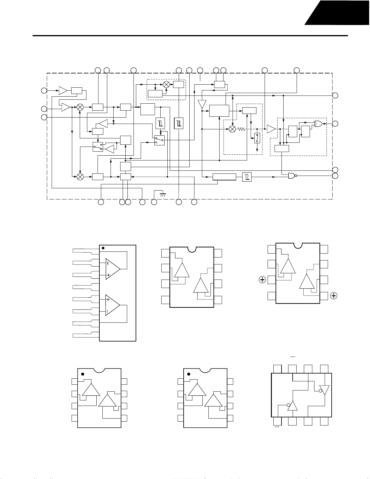
Harman Kardon
Dolby Digital Audio/Video Receiver
43 2 1 24 23 22 21 20 19
IN
PUT
6
5
7
AGC
BPF
LPF
LPF
INTEGRATED CIRCUIT DIAGRAMS 11
Q901 - LA2232 RDS MODULATOR
ARI-DK DET
LPF LEVEL
DIV
-DET
LPF BPF
D-PLL
V
CC
CLOCK
RECOVERY
BI-PHASE DEMOD.
LOGIC
LOGIC
DIFF. DECODE
DFF DFF
AVR75/85
CLK
18
DATA
17
E-OR
VCO
LPF
QD02, 32, 52, QM08 - 4560M OP-AMP
LPF
NJM
LEVEL-DET
141312111098
SK-IDDK-ID
Q301, QE01-03, QC01-10, QE07-12, QC12, QL91, QS01-03,
QW01, QS13, QS51-54, QF02, 03, QG55, 56 NJM4558DD - OP-AMP
A OUTPUT
A -INPUT
A +INPUT
V-
B +INPUT
B -INPUT
B OUTPUT
V+
QK02, QK03 - NJM2115M
1
2
3
4
5
6
7
8
OP-AMP
A OUTPUT
A
A +INPUT
A -INPUT
1
2
A
+
-
3
V
-
4
B
+
V
+
8
B OUTPUT
7
B -INPUT
6
-
B +INPUT
5
B
QW01 - NJM2115M
DUAL OP-AMP
A OUTPUT
A -INPUT
V
SS
AND
QM04 - MC14577C
VIDEO AMP
1
2
A
+
-
3
4
8
7
6
B
+
-
5
Q609 - TCW125FU
DUAL BUS BUFFER
V
CC
8
G2
7
Y1 A2
6
5
SK-ADJ.
16
15
RDS-ID
V
DD
B OUTPUT
B -INPUT
A OUTPUT
A -INPUT A -INPUT
11
AA
22
88
V+
77
B OUTPUT
A OUTPUT
BB
A +INPUT A +INPUT
33
V- V-
44
66
B -INPUT
55
B +INPUT
V+
B OUTPUT
B -INPUT
B +INPUT
G1
1
2
A1 Y2
4
3
GND
71
Page 74

Harman Kardon
Dolby Digital Audio/Video Receiver
AVR75/85 WIRING DIAGRAM (120V & 230V)
AVR75/85
A
B
AVR75/85 120V and 230V Wiring Connection
C
D
1
2
3
E
1
2
3
4
5
6
7
4
5
6
7
A
B
C
D
E
72
Page 75
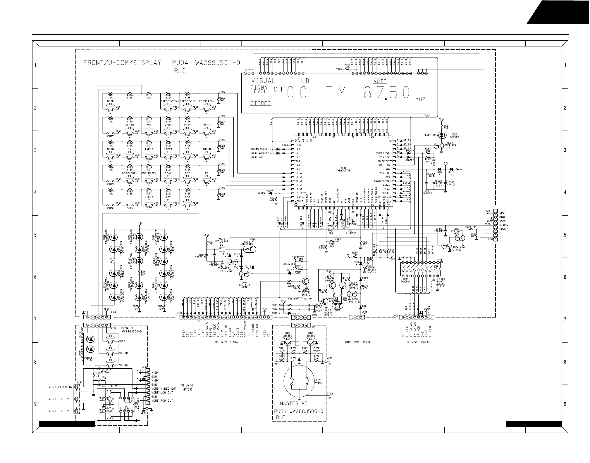
Harman Kardon
Dolby Digital Audio/Video Receiver
AVR75 (120V) SCHEMATIC DIAGRAM 1 of 8 (FRONT PCB PU04, MASTER VOLUME PCB PU54, AUX IN PL94)
AVR75/85
J
4.9
0
LMK
FROM JB04
(PB04)
-30
4.9
-33
-33
4.8
-33
4.9
HGF
-30
4.7
-33
2.7
-28
2.7
-30
I
0
4.9
0
0
4.7
0
0
0
1.1
0
0
5.5
4.9
4.9
4.9
0.2
4.9
4.9
4.9
EDCBA
-30
-26
-28
-30
-30
-33
-33
-28
-34
0.6
0.6
0
0
0
0
0
1.2
4.9
0
1.1
4.9
0.5
4.8
4.8
4.8
0.0
0.0
0.0
5.5
5.5
5.5
4.8
5.0
0
0.2
5.5
5.5
5.4
0.4
0
4.9
0.3
4.9
0
4.9
00
4.8
0.6
4.9
5.5
5.5
0
0
0
0
0.6
1.2
0
0
20.3
21.0
0
0
5.0
0
0
0
5.0
5.0
AVR75 US 120V
Schematic 1 of 8
TEST VOLTAGES SHOWN IN RED
0.0
0.0
0.0
AVR75/85 PAGE 73-1of2
ABCDE
FGH
AVR75/85PAGE73-2of2
J
K
LMI
73
Page 76

Harman Kardon
Dolby Digital Audio/Video Receiver
AVR75/85
AVR75 (120V) SCHEMATIC DIAGRAM 2 of 8 (TUNER PCB P104)
ANTENNA
TERMINAL
2.3
2.3
J
14.2
0.1
0.2
0.1
0.6
2.5
4.8
0
0
4.8
1.1
0
0.6
0.8
0.7
0
LMK
5.3
5.5
5.9
HGF
I
1.5
EDCBA
1.5
0
0
0
0
10.8
8.5
2.1
13.3
1.4
1.6
3.6
5.4
5.4
2.8
1.5
6.9
3.6
6.9
3.6
1.1
6.9
AVR75/85 PAGE 74-1of2
AB CDE
FGH
AVR75 US 120V
Schematic 2 of 8
TEST VOLTAGES SHOWN IN RED
J
K
AVR75/85 PAGE 74-2of2
LMI
74
Page 77

Harman Kardon
Dolby Digital Audio/Video Receiver
AVR75/85
AVR75 (120V) SCHEMATIC DIAGRAM 4 of 8 (AC-3 CROSSOVER PCB PC04, TONE CONTROL PCB PF04, VIDEO SELECTOR PCB PL04, S-VIDEO PCB PL54)
AVR75/85 PAGE 76-1of4
AVR75 US 120V
Schematic 4 of 8
TEST VOLTAGES SHOWN IN RED
000
000
000
EDCBA
HGF
0
0
I
0
0
0
0
0
0
J
0
0
0
LMK
AVR75/85 PAGE 76-2of4
0
0
0
0
0
0
0
0
0
0
0
0
0
00
0
00
0
000
00
000
000
000
00000000000
00000000000
8.6
4.9
8.6
000
000
000
000
000
4.9
0.6
0.6
3.0
0
0
0
0
0
0
000
0
0
0
0
0
0
0
4.8
1.5
0.9
0
0
2.9
2.9
0
4.8
0.9
1.5
1.3
2.3
0.4
0
2.1
1.6
2.1
1.5
1.5
2.1
2.1
000
000
000
000
000
000
000
4.9
0.6
0.6
4.8
2.2
0.8
2.2
2.1
4.5
2.2
4.2
1.9
0.3
4.8
1.9
4.8
4.8
2.3
2.3
4.8
4.9
1.8
4.9
1.8
0.5
0.9
4.8
1.5
4.8
AVR75/85 PAGE 76-3of4
ABCDE
000
8.9
0.6
0.6
FGH
AVR75/85 PAGE 76-4of4
J
K
LMI
76
Page 78

Harman Kardon
Dolby Digital Audio/Video Receiver
AVR75/85
AVR75 (120V) SCHEMATIC DIAGRAM 5 of 8 (CONNECT PCB PY04)
AVR75 US 120V
Schematic 5 of 8
TEST VOLTAGES ARE SHOWN IN RED
0
0
0.6
0.6
5.6
4.8
-13.3
-13.3
-13.3
EDCBA
4.8
4.8
4.8
4.8
2.8
0
0
0
0
4.3
4.9
0
2.8
0000000
3.0
2.8
4.9
HGF
4.8
4.9
0
4.8
000
I
J
14.4
LMK
0
0
0
4.8
0
-14.7V
0
0
-13.3
AVR75/85 PAGE 77-1of2
4.8
0
AB CDE
FGH
AVR75/85PAGE77-2of2
J
K
LMI
77
Page 79

Harman Kardon
Dolby Digital Audio/Video Receiver
AVR75/85
AVR75 (120V) SCHEMATIC DIAGRAM 6 of 8 (VOLTAGE AMP PCB - P714, MAIN PCB - P704, SURROUND AMP PCB - PP04,
SPEAKER TERMINAL PCB - P754, HEADPHONE PCB - PW04, SPEAKER PROTECT PCB - PN54, STANDBY PCB - PB04, POWER SWITCH PCB - PU94)
AVR75/85 PAGE 78-1of4
0
0
0
-15.0
0
0
0
15.0
-1.3
-40.2
-43.0
-42.3
J
+44.3
-41.8
0.6
+43.3
-43.0
+44.3
-41.9
0.7
-0.1
-0.1
-0.1
-0.1
LMK
AVR75/85 PAGE 78-2of4
+44.3V
-44.1V
43.4
HGF
I
EDCBA
1.2
-1.2
42.1
-42.0
1.2
-1.2
-0.6
-0.6
0.4
1.2
0
-1.2
42.5
0.6
-0.6
-42.3
-43.0
43.2
0.6
-0.6
0
0
-43.0
0
0
0
0
42.1
41.5
0
0
-0.6
-1.0
-40.7
-42.3
40.8
41.4
1.2
1.2
-41.3
19.6
-0.7
-0.6
1.2
-1.2
-0.6
1.2
-1.2
AC 17.0
AC 8.1
0.0
AC 8.1
AC 18.0
-21.3
-0.6
-0.6
0.4
0.4
21.6
-7.4
1.2
0
-1.2
1.2
0
-1.2
42.5
0.6
-0.6
-42.3
-43.0
42.5
0.6
-0.6
-42.3
-25.0
-25.0
42.1
1.2
-1.2
-42.0
42.1
1.2
-1.2
-42.0
-42.0
40.8
42.1
41.5
-0.6
-0.6
0
-1.0
-1.0
-42.3
-42.3
-5.2
0.4
0
41.5
-40.7
42.1
00
-40.7
-5.2
0
-40.2
-1.3
-1.3
0
0
0
-0.6
0
-0.6
0
0
-42.3
-43.0
-40.2
-42.3
-43.0
-39.8
40.8
21.3
1.2
1.2
-41.3
41.4
1.2
1.2
5.6
5.6
41.4
-41.3
43.2
43.2
0.6
-0.6
-43.0
0.6
-0.6
15.2
-15.3
43.2
0
-43.0
43.2
0
0
-43.0
0
00
0
0
15.1
-15.1
5.0
43.4
0
0
14.0
28.1
43.4
0
0
43.0
21.6
20.8
21.7
1.0
21.5
-5.2
43.2
43.4
42.7
44.3
-0.4
21.6
1.0
21.4
1.0
0
-7.4
16.2V
8.0V
8.0V
16.2V
AVR75/85 PAGE 78-3of4
AB CDE
21.5
19.9
5.6
-33.8
19.9
-10.0
-4.9
5.09.3
-26.2
-43.0
AC 34.0V
AC 33.1V0
-44.1
0V
AC 33.1V
FGH
AC 34.0V
+44.3V
-44.1V
J
K
0
0
1.3
00
0
AVR75 US 120V
Schematic 6 of 8
TEST VOLTAGES SHOWN IN RED
AVR75/85 PAGE 78-4of4
LMI
78
Page 80
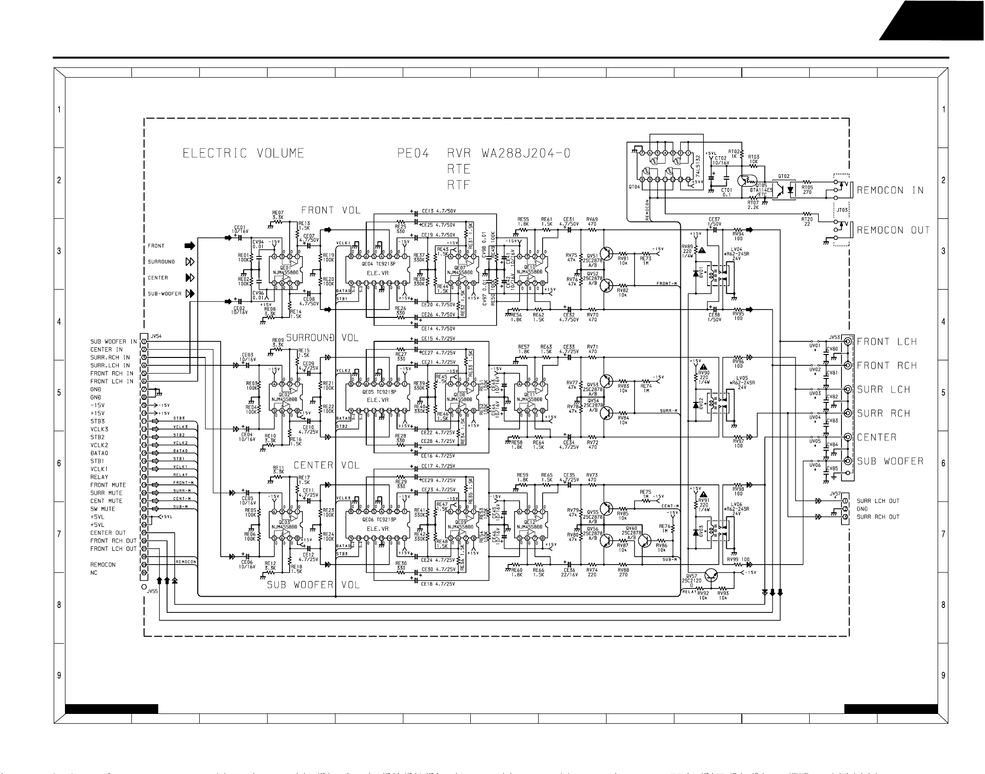
Harman Kardon
Dolby Digital Audio/Video Receiver
AVR75/85
AVR75 (120V) SCHEMATIC DIAGRAM 7 of 8 (ELECTRONIC VOLUME PCB - PE04)
EDCBA
HGF
I
0
000
4.5
J
4.8
4.8
0
10.6
0
0
0
LMK
FROM JY06 (PY04)
AVR75/85 PAGE 79-1of2
ABCDE
FGH
-14.8
10.6
10.6
TO
JP01
(PP04)
-14.0
AVR75 US 120V
Schematic 7 of 8
TEST VOLTAGES SHOWN IN RED
AVR75/85PAGE79-2of2
J
K
LMI
79
Page 81
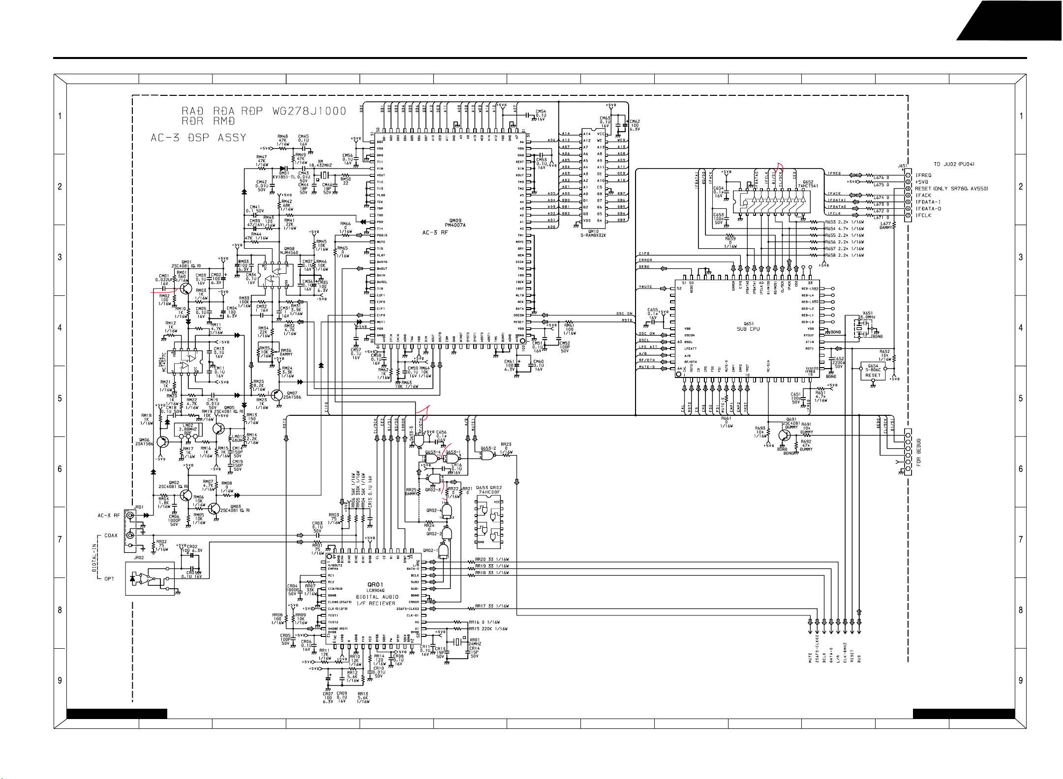
Harman Kardon
Dolby Digital Audio/Video Receiver
AVR75/85
AVR75 (120V/230V) SCHEMATIC DIAGRAM 8 of 8 (AC-3/DSP PCB - P604)
0.8
0.1
000
000
5.0
1.9
0.7
2.3
1.9
2.5
2.3
J
LMK
4.8
5.0
5.0
5.0
4.7
5.0
0
0
2.5
5.0
5.0
4.7
4.7
0
4.7
5.0
4.9
5.0
4.9
2.2
2.2
5.0
0.5
2.5
5.0
5.0
5.0
5.0
5.0
5.0
5.0
HGF
0
0
0
0
0
1.6
0.1
5.0
0.1
0.1
5.0
I
5.0
5.0
5.0
EDCBA
0
0
0
5.0
0
5.0
5.0
5.0
5.0
5.0
5.0
5.0
0
5.0
0
5.0
2.1
2.5
0
5.0
DEMODULATOR
5.0
5.0
2.3
0
4.5
4.8
4.8
0
5.0
0
5.0
0
0
0
0
0
0
0
5.0
5.0
5.0
5.0
0
0
0
0
0
0
0
0
0
0
5.0
0
5.0
5.0
0
5.0
5.0
0
0
0
0
5.0
5.0
5.0
5.0
0
0.6
4.9
0
0
-1.0
4.9
-0.3
5.0
0
0
5.0
3.9
0
0
2.7
2.5
5.0
4.8
2.5
4.3
2.4
2.4
4.9
2.2
0
5.0
5.0
0
2.5
0
2.1
0
5.0
5.0
2.2
0
0
0
0
0
5.0
5.0
AVR75 US 120V & European 230V
Schematic 8 of 8
CA-3 DSP ASSY
TEST VOLTAGES SHOWN IN RED
AVR75/85 PAGE 80-1of2
ABCDE
FGH
AVR75/85 PAGE 80-2of2
J
K
LMI
80
Page 82

Harman Kardon
Dolby Digital Audio/Video Receiver
AVR75 (230V) SCHEMATIC DIAGRAM 1 of 7 (FRONT PCB - PU04, MASTER VOLUME PCB - PU54, AUX IN - PL94)
AVR75/85
EDCBA
HGF
I
J
LMK
AB CDE
FGH
AVR75 European 230V
Schematic 1 of 7
J
K
LMI
81
Page 83
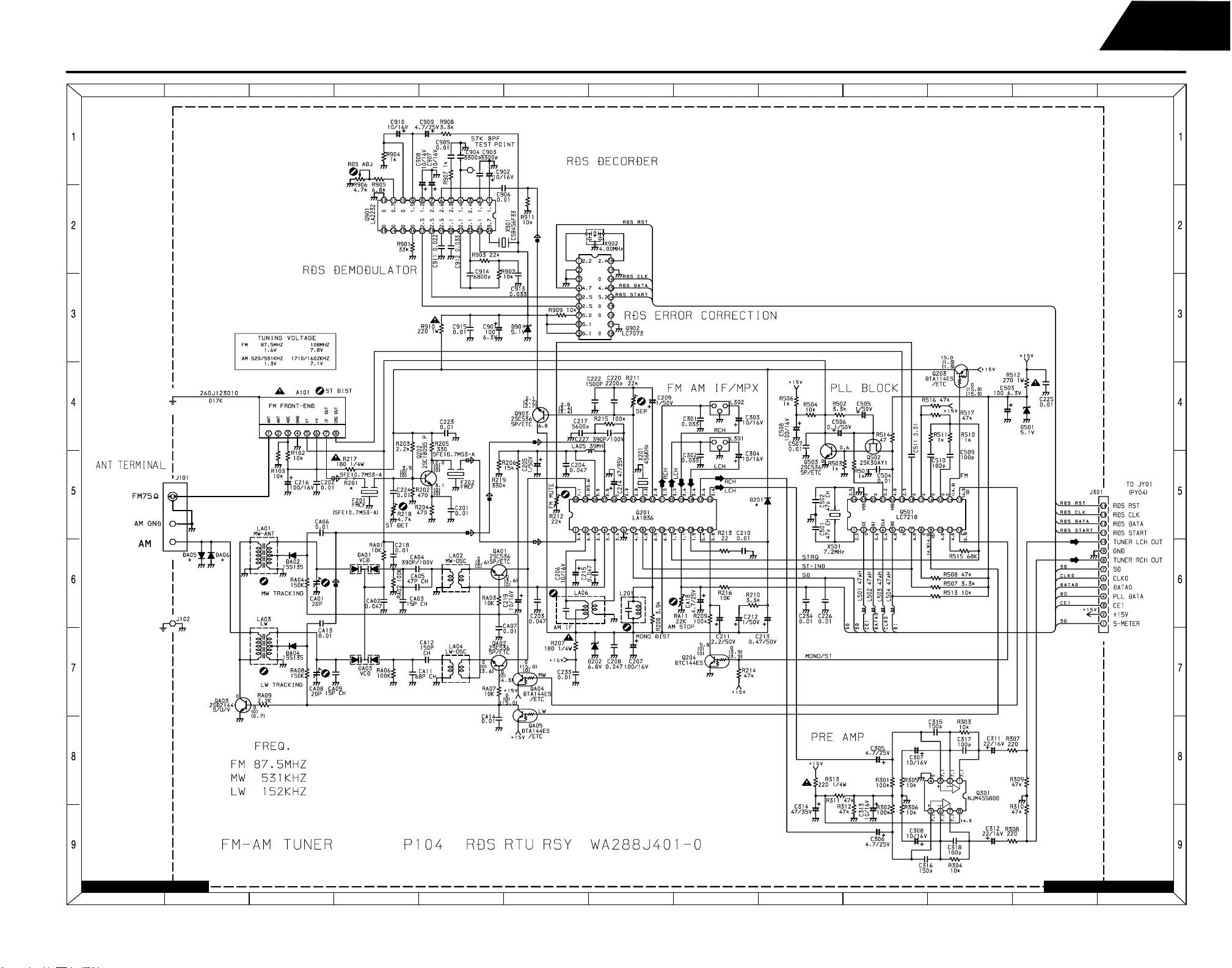
Harman Kardon
Dolby Digital Audio/Video Receiver
AVR75/85
AVR75 (230V) SCHEMATIC DIAGRAM 2 of 7 (TUNER PCB - P104)
EDCBA
HGF
I
J
LMK
AVR75 European 230V
Schematic 2 of 7
AVR75/85 PAGE 82-1of2
ABCDE
FGH
AVR75/85 PAGE 82-2of2
J
K
LMI
82
Page 84
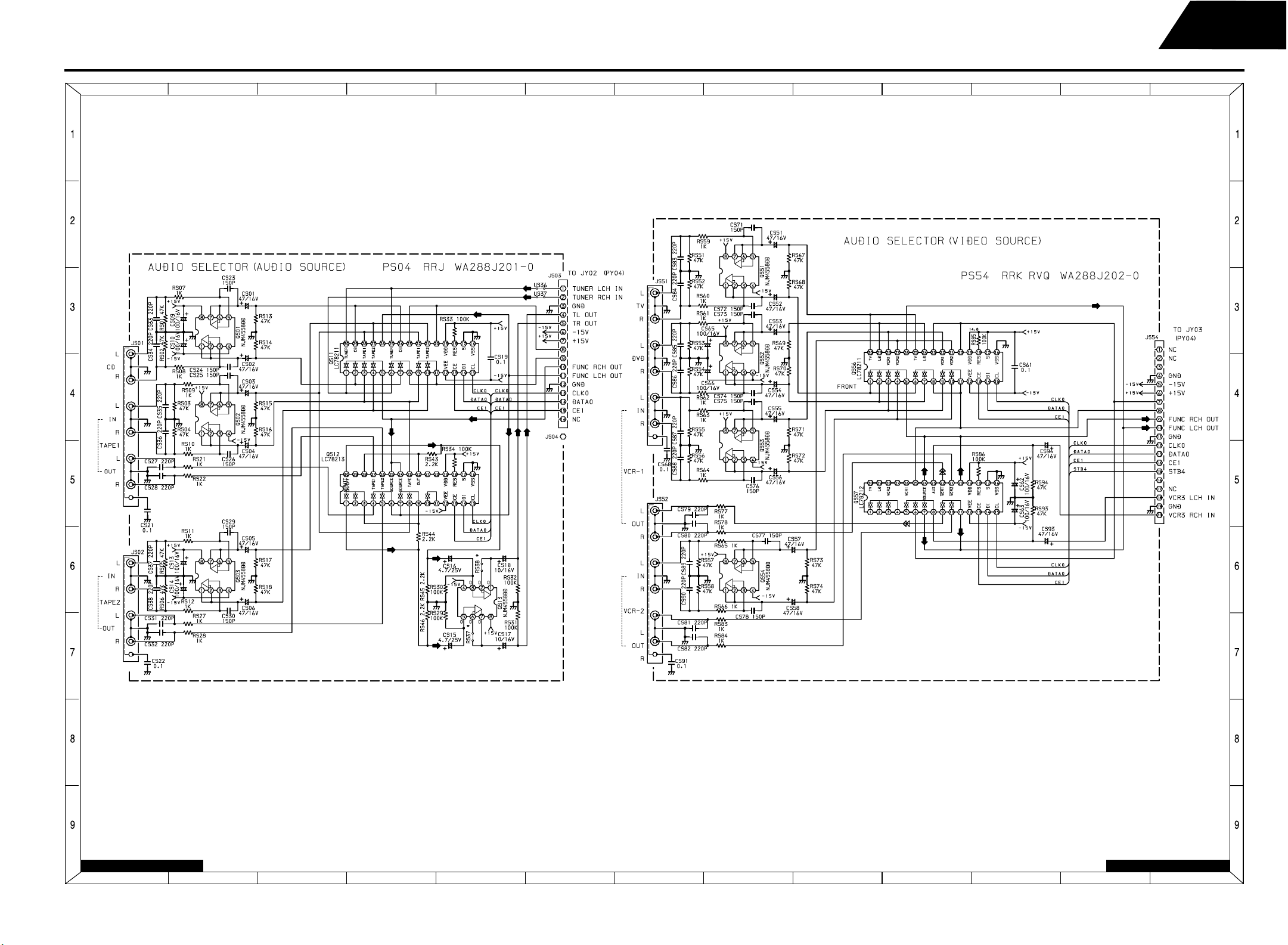
Harman Kardon
Dolby Digital Audio/Video Receiver
AVR75/85
AVR75 (230V) SCHEMATIC DIAGRAM 3 of 7 (AUDIO SELECTOR PCB - PS04, AUDIO/VIDEO PCB - PS54)
EDCBA
HGF
I
J
LMK
AVR75/85 PAGE 83-1of2
AB CDE
FGH
AVR75 European 230V
Schematic 3 of 7
J
K
LMI
AVR75/85 PAGE 83-2of2
83
Page 85
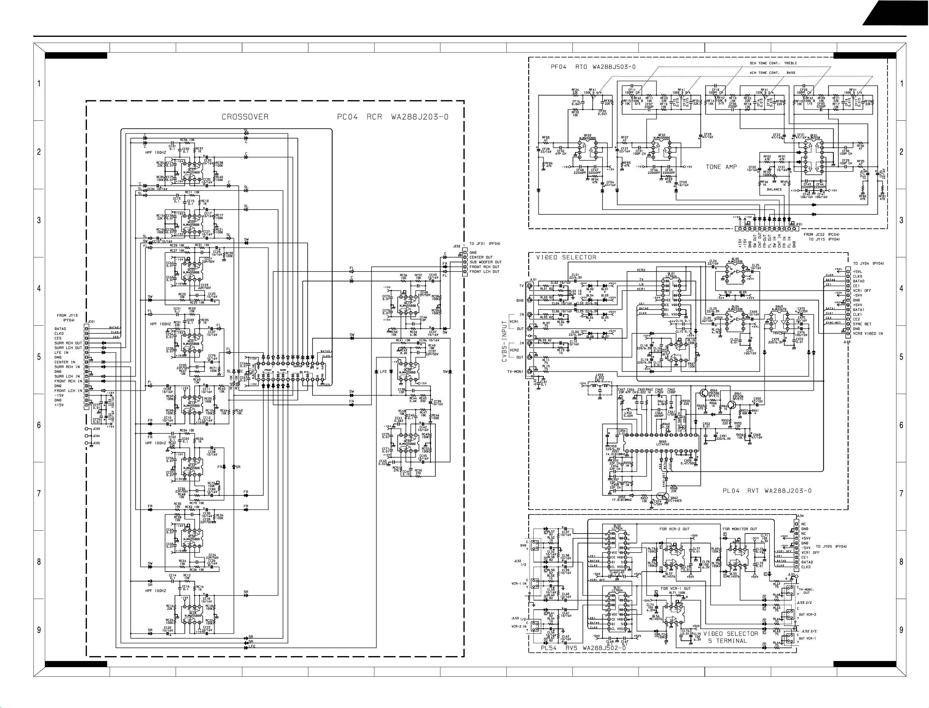
Harman Kardon
Dolby Digital Audio/Video Receiver
AVR75/85
AVR75 (230V) SCHEMATIC DIAGRAM 4 of 7 (AC-3 CROSSOVER PCB - PC04, TONE CONTROL PCB - PF04, VIDEO SELECTOR PCB - PL04, S-VIDEO PCB - PL54)
AVR75/85 PAGE 84 - 1 of 4
AVR75 European 230V
Schematic 4 of 7
EDCBA
HGF
I
J
LMK
AVR75/85 PAGE 84 - 2 of 4
AVR75/85 PAGE 84 - 3 of 4
AB CDE
FGH
AVR75/85 PAGE 84 - 3 of 4
J
K
LMI
84
Page 86
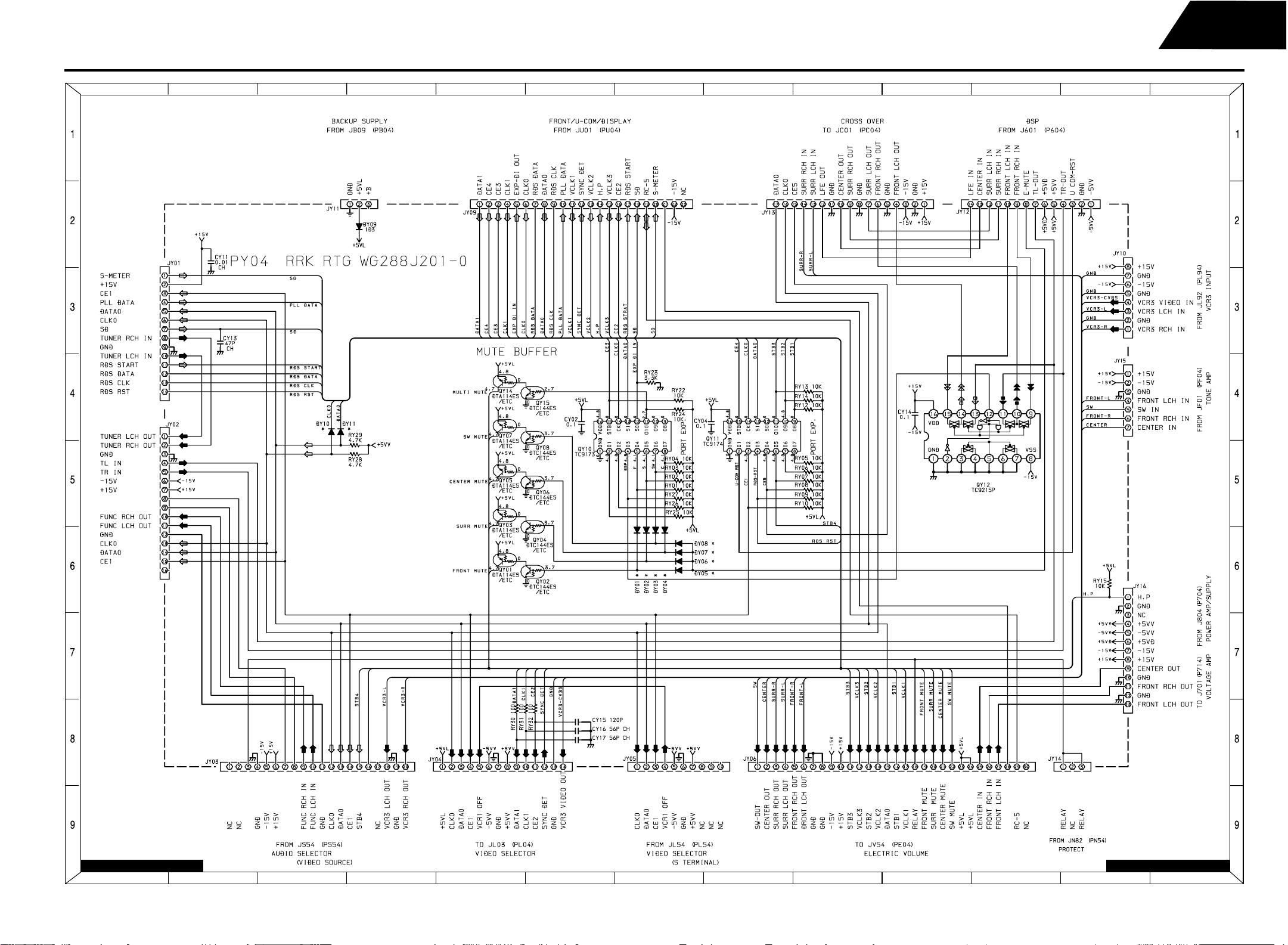
Harman Kardon
Dolby Digital Audio/Video Receiver
AVR75/85
AVR75 (230V) SCHEMATIC DIAGRAM 5 of 7 (CONNECT PCB PY04)
AVR75
European 230V
Schematic 5 of 7
EDCBA
HGF
I
J
LMK
AVR75/85 PAGE 85-1of2
AB CDE
FGH
AVR75/85 PAGE 85-2of2
J
K
LMI
85
Page 87
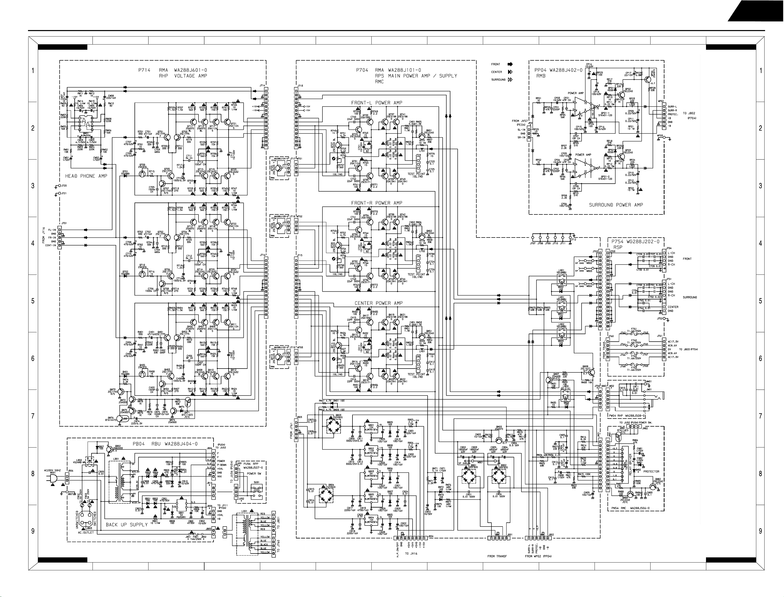
Harman Kardon
Dolby Digital Audio/Video Receiver
AVR75 (230V) SCHEMATIC DIAGRAM 6 of 7 (VOLTAGE AMP PCB - P714, MAIN PCB - P704, SURROUND AMP PCB - PP04, SPEAKER TERMINAL - P754, HEADPHONE PCB - PW04, SPEAKER PROTECT PCB - PN54, STANDBY PCB - PB04, POWER SWITCH PCB - PU94)
AVR75/85
AVR75/85 PAGE 86-1of4
EDCBA
HGF
I
J
LMK
AVR75/85 PAGE 86-2of4
AVR75/85 PAGE 86-3of4
AB CDE
FGH
AVR75 European 230V
Schematic 6 of 7
AVR75/85 PAGE 86-4of4
J
K
LMI
86
Page 88
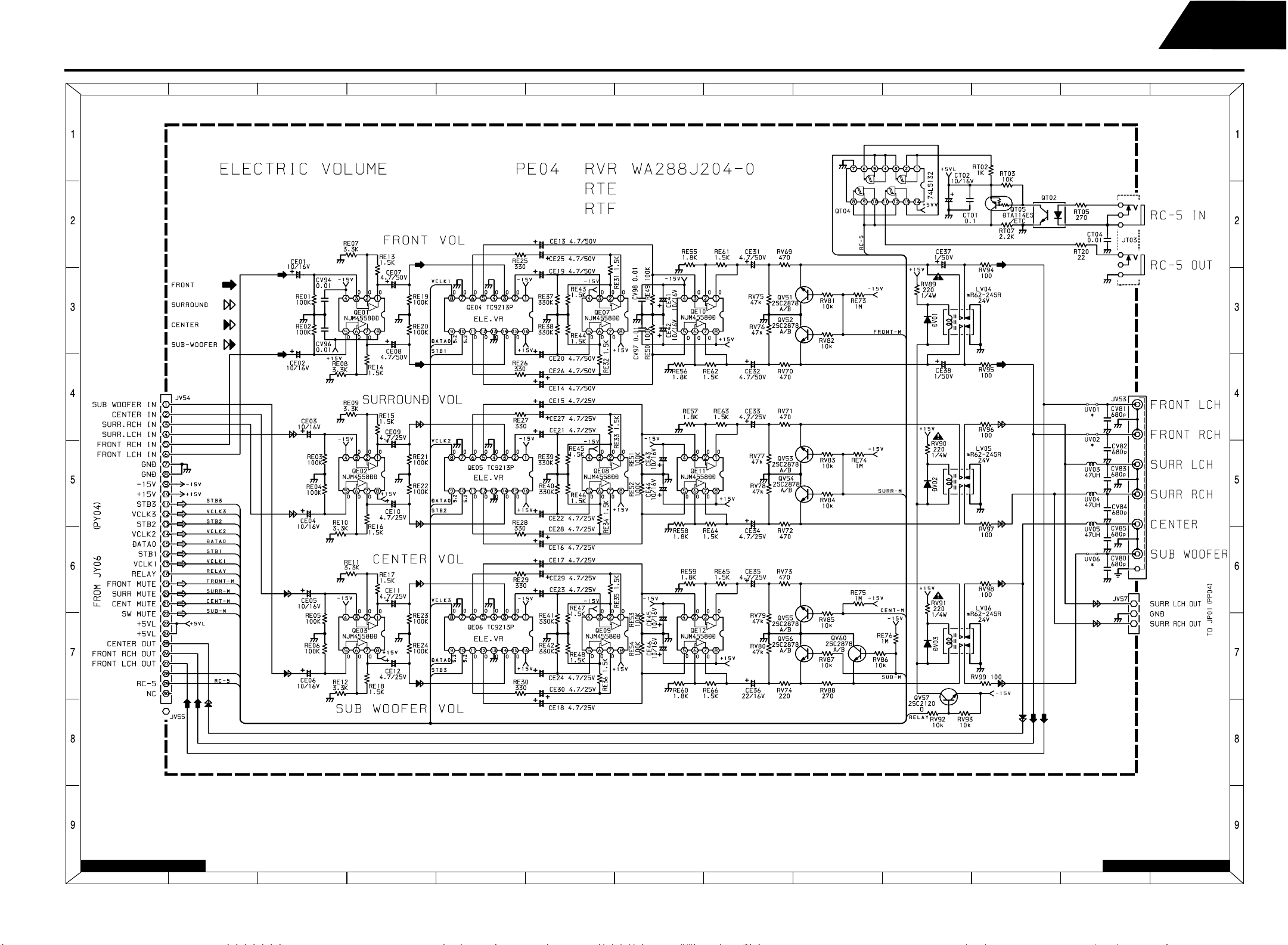
Harman Kardon
Dolby Digital Audio/Video Receiver
AVR75/85
AVR75 (230V) SCHEMATIC DIAGRAM 7 of 7 ELECTRONIC VOLUME CONTROL PCB, PE04
EDCBA
HGF
I
J
LMK
AVR75/85PAGE87-1of2
ABCDE
FGH
AVR75 European 230V
Schematic 7 of 7
J
K
AVR75/85 PAGE 87 - 2 of 2
LMI
87
Page 89

Harman Kardon
Dolby Digital Audio/Video Receiver
AVR85 (120V) SCHEMATIC DIAGRAM 1 of 8 (FRONT PCB - PU04, MASTER VOLUME PCB - PU54, AUX IN - PL94)
AVR75/85
AVR75/85 PAGE 88-1of2
EDCBA
HGF
I
J
LMK
AB CDE
FGH
AVR85 US 120V
Schematic 1 of 8
AVR75/85 PAGE 88 - 2 of 2
J
K
LMI
88
Page 90

Harman Kardon
Dolby Digital Audio/Video Receiver
AVR75/85
AVR85 (120V) SCHEMATIC DIAGRAM 2 of 8 (TUNER PCB - P104)
EDCBA
HGF
I
J
LMK
ANTENNA TERMINAL
AVR85 US 120V
Schematic 2 of 8
AVR75/85 PAGE 89-1of2
ABCDE
FGH
AVR75/85 PAGE 89-2of2
J
K
LMI
89
Page 91
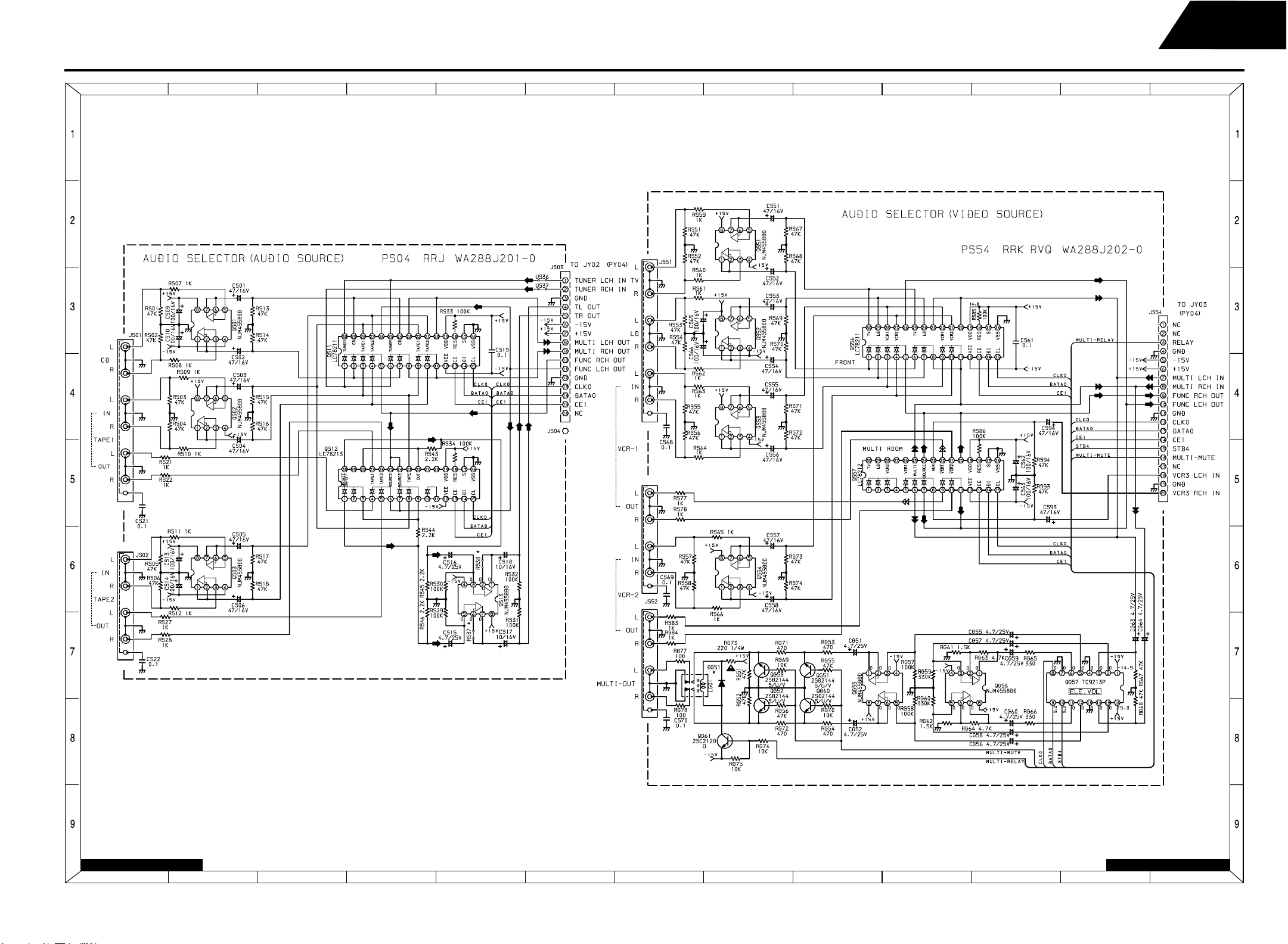
Harman Kardon
Dolby Digital Audio/Video Receiver
AVR75/85
AVR85 (120V) SCHEMATIC DIAGRAM 3 of 8 (AUDIO SELECTOR PCB - PS04, AUDIO/VIDEO PCB - PS54)
EDCBA
HGF
I
J
LMK
AVR75/85 PAGE 90-1of2
AB CDE
FGH
AVR85 US 120V
Schematic 3 of 8
AVR75/85 PAGE 90-2of2
J
K
LMI
90
Page 92

Harman Kardon
Dolby Digital Audio/Video Receiver
AVR75/85
AVR85 (120V) SCHEMATIC DIAGRAM 4 of 8 (AC-3 CROSSOVER PCB - PC04, TONE CONTROL PCB - PF04, VIDEO SELECTOR PCB - PL04, S-VIDEO PCB - PL54)
AVR75/85 PAGE 91 - 1 of 4
AVR85 US 120V
Schematic 4 of 8
EDCBA
HGF
I
J
LMK
AVR75/85 PAGE 91 - 2 of 4
AVR75/85 PAGE 91 - 3 of 4
AB CDE
FGH
AVR75/85 PAGE 91 - 4 of 4
J
K
LMI
91
Page 93

Harman Kardon
Dolby Digital Audio/Video Receiver
AVR75/85
AVR85 (120V) SCHEMATIC DIAGRAM 5 of 8 (CONNECT PCB - PY04)
AVR85 US 120V
Schematic 5 of 8
EDCBA
HGF
I
J
LMK
AVR75/85 PAGE 92-1of2
AB CDE
FGH
AVR75/85 PAGE 92-2of2
J
K
LMI
92
Page 94

Harman Kardon
Dolby Digital Audio/Video Receiver
AVR85 (120V) SCHEMATIC DIAGRAM 6 of 8 (VOLTAGE AMP PCB - P714, MAIN PCB - P704, SURROUND AMP PCB - PP04, SPEAKER TERMINAL - P754,
HEADPHONE PCB - PW04, SPEAKER PROTECT PCB - PN54, STANDBY PCB - PB04, POWER SWITCH PCB - PU94)
AVR75/85
AVR75/85 PAGE 93-1of4
EDCBA
HGF
I
J
LMK
AVR75/85 PAGE 93-2of4
AVR75/85 PAGE 93-3of4
ABCDE
FGH
AVR85 US 120V
Schematic 6 of 8
AVR75/85 PAGE 93-4of4
J
K
LMI
93
Page 95

Harman Kardon
Dolby Digital Audio/Video Receiver
AVR75/85
AVR85 (120V) SCHEMATIC DIAGRAM 7 of 8 (ELECTRONIC VOLUME PCB - PE04)
AVR85 US 120V
Schematic 7 of 8
EDCBA
HGF
I
J
LMK
AVR75/85 PAGE 94-1of2
ABCDE
FGH
AVR75/85 PAGE 94-2of2
J
K
LMI
94
Page 96
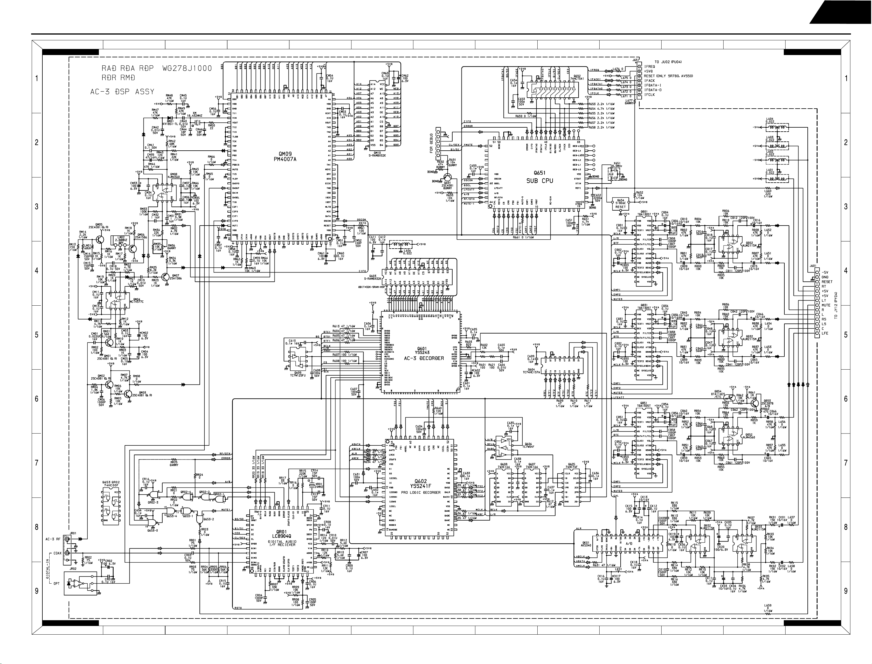
Harman Kardon
Dolby Digital Audio/Video Receiver
AVR75/85
AVR85 (120V & 230v) SCHEMATIC DIAGRAM 8 of 8 (AVR85 DSP BOARD - P604)
AVR75/85 PAGE 95-1of4
AC-3 RF DEMODULATOR
EDCBA
HGF
I
J
LMK
AVR75/85 PAGE 95 - 2 of 4
AVR85 US 120V
Schematic 8 of 8
AVR75/85 PAGE 95-3of4
AB CDE
FGH
AVR75/85 PAGE 95 - 4 of 4
J
K
LMI
95
Page 97
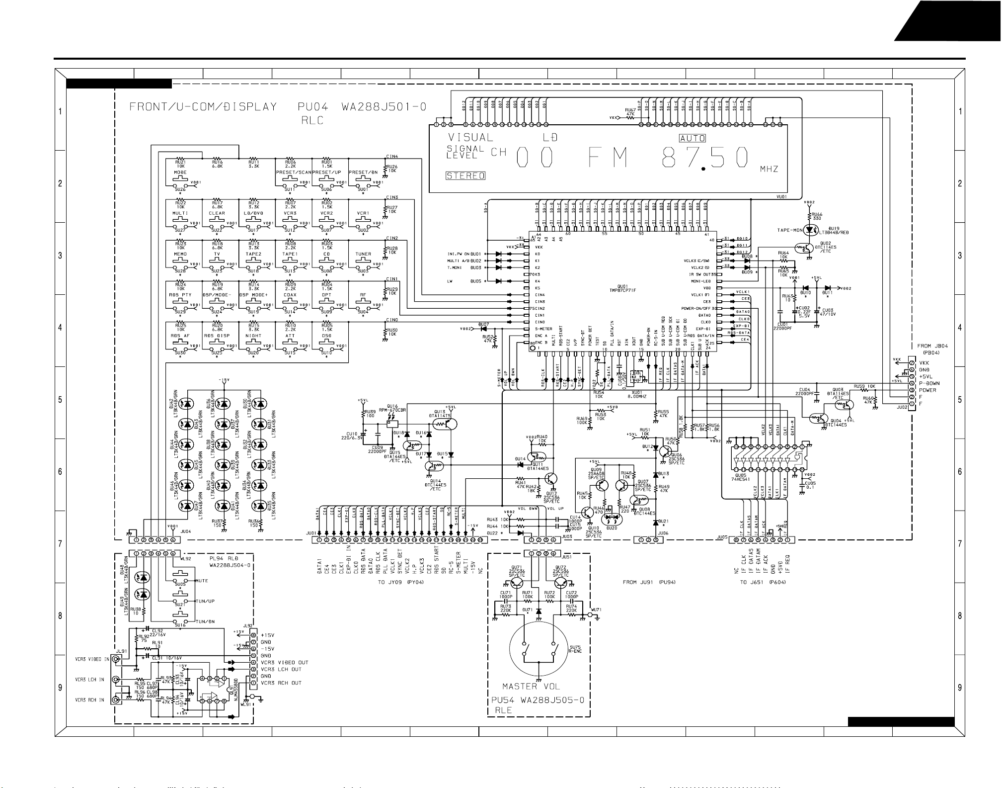
Harman Kardon
Dolby Digital Audio/Video Receiver
AVR85 (230V) SCHEMATIC DIAGRAM 1 of 8 (FRONT PCB - PU04, MASTER VOLUME PCB - PU54, AUX IN - PL94)
AVR75/85
AVR75/85 PAGE 96 - 1 of 2
EDCBA
HGF
I
J
LMK
ABCDE
FGH
AVR85 European 230V
Schematic 1 of 8
AVR75/85 PAGE 96-2of2
J
K
LMI
96
Page 98
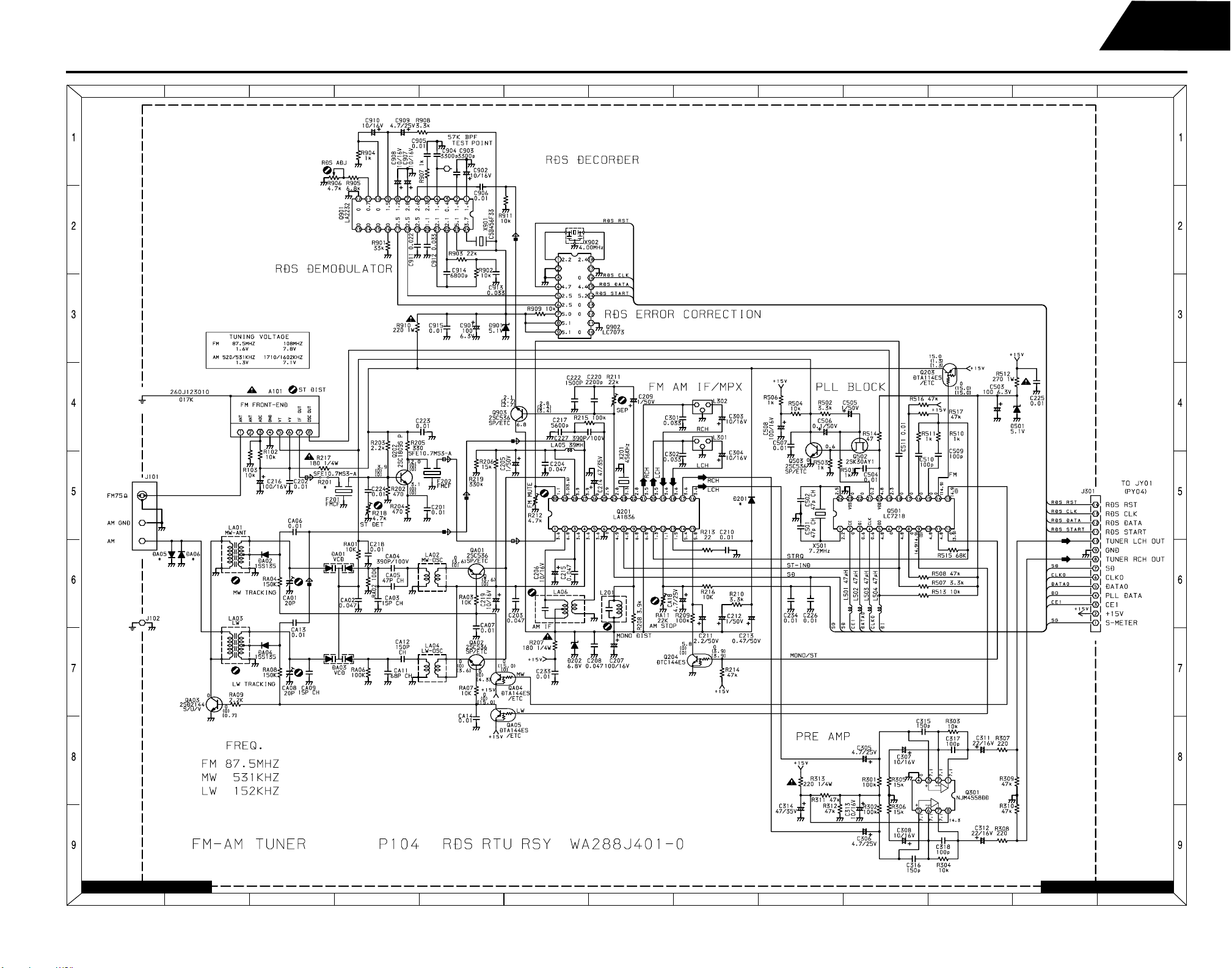
Harman Kardon
Dolby Digital Audio/Video Receiver
AVR75/85
AVR85 (230V) SCHEMATIC DIAGRAM 2 of 8 (TUNER PCB - P104)
EDCBA
HGF
I
J
LMK
AVR85 European 230V
Schematic 2 of 8
ANT TERMINAL
AVR75/85 PAGE 97 - 1 of 2
ABCDE
FGH
AVR75/85 PAGE 97-2of2
J
K
LMI
97
Page 99
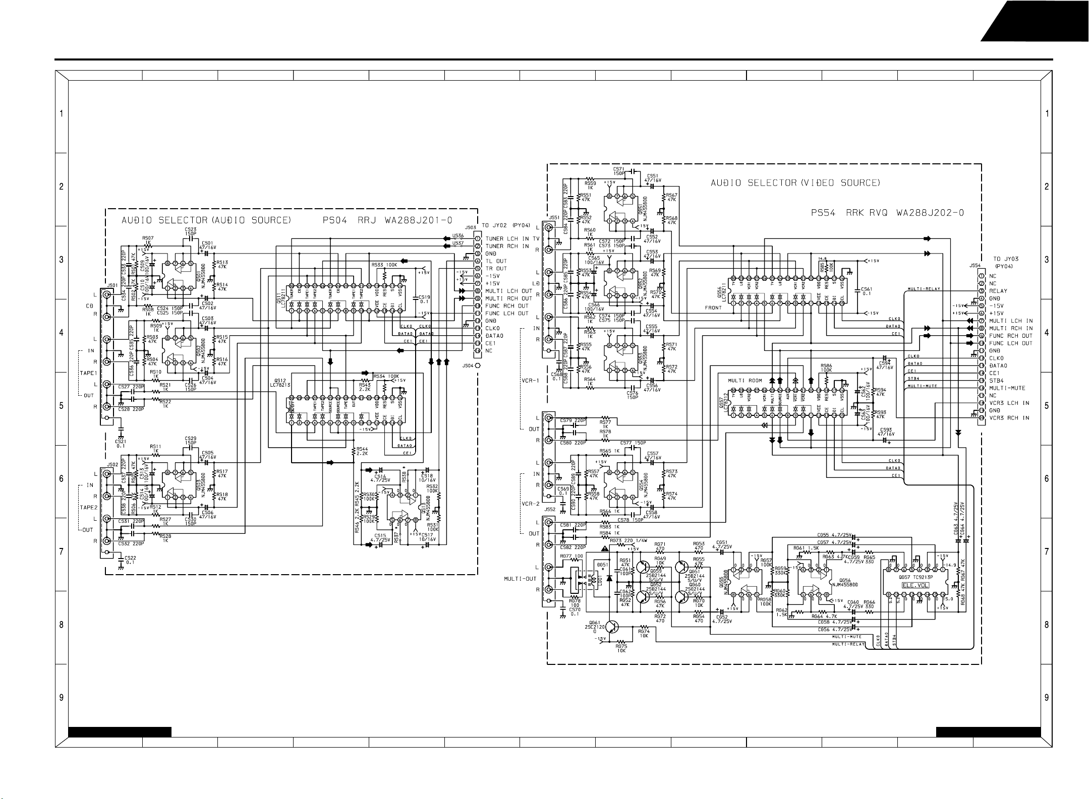
Harman Kardon
Dolby Digital Audio/Video Receiver
AVR75/85
AVR85 (230V) SCHEMATIC DIAGRAM 3 of 8 (AUDIO SELECTOR PCB - PS04, AUDIO/VIDEO PCB PS54)
EDCBA
HGF
I
J
LMK
AVR75/85 PAGE 98-1of2
AB CDE
FGH
AVR85 European 230V
Schematic 3 of 8
AVR75/85 PAGE 98-2of2
J
K
LMI
98
Page 100
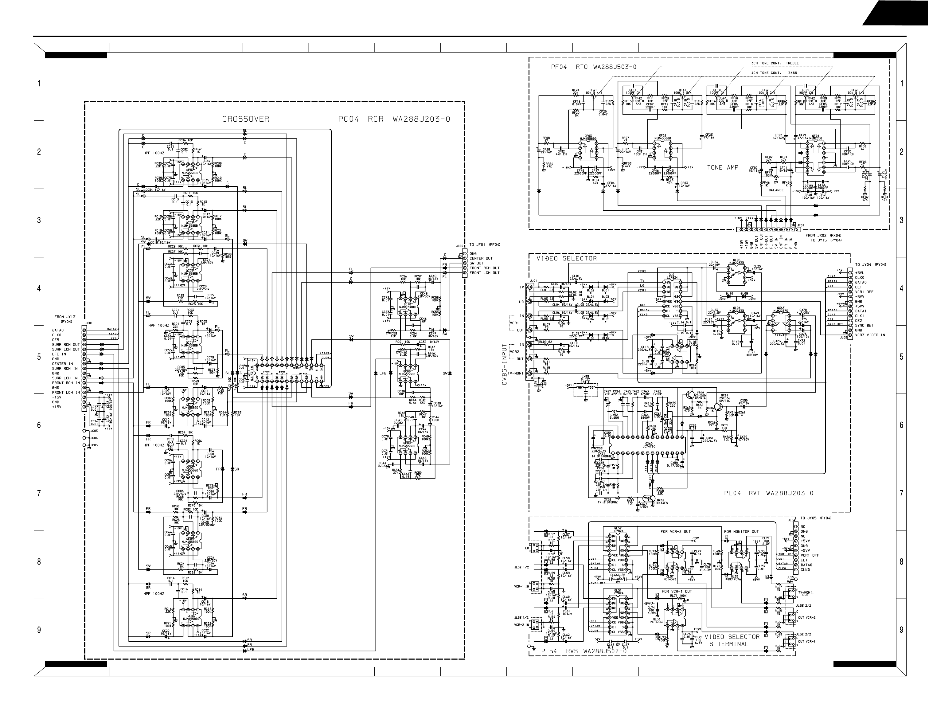
Harman Kardon
Dolby Digital Audio/Video Receiver
AVR75/85
AVR85 (230V) SCHEMATIC DIAGRAM 4 of 8 (AC-3 CROSSOVER PCB - PC04, TONE CONTROL PCB - PF04, VIDEO SELECTOR PCB - PL04, S-VIDEO PCB PL54)
AVR75/85 PAGE 99 - 1 of 4
AVR85 European 230V
Schematic 4 of 8
EDCBA
HGF
I
J
LMK
AVR75/85 PAGE 99-2of4
AVR75/85 PAGE 99 - 3 of 4
ABCDE
FGH
AVR75/85 PAGE 99-4of4
J
K
LMI
99
 Loading...