

Page 1
Data Sheet
October 5, 2009
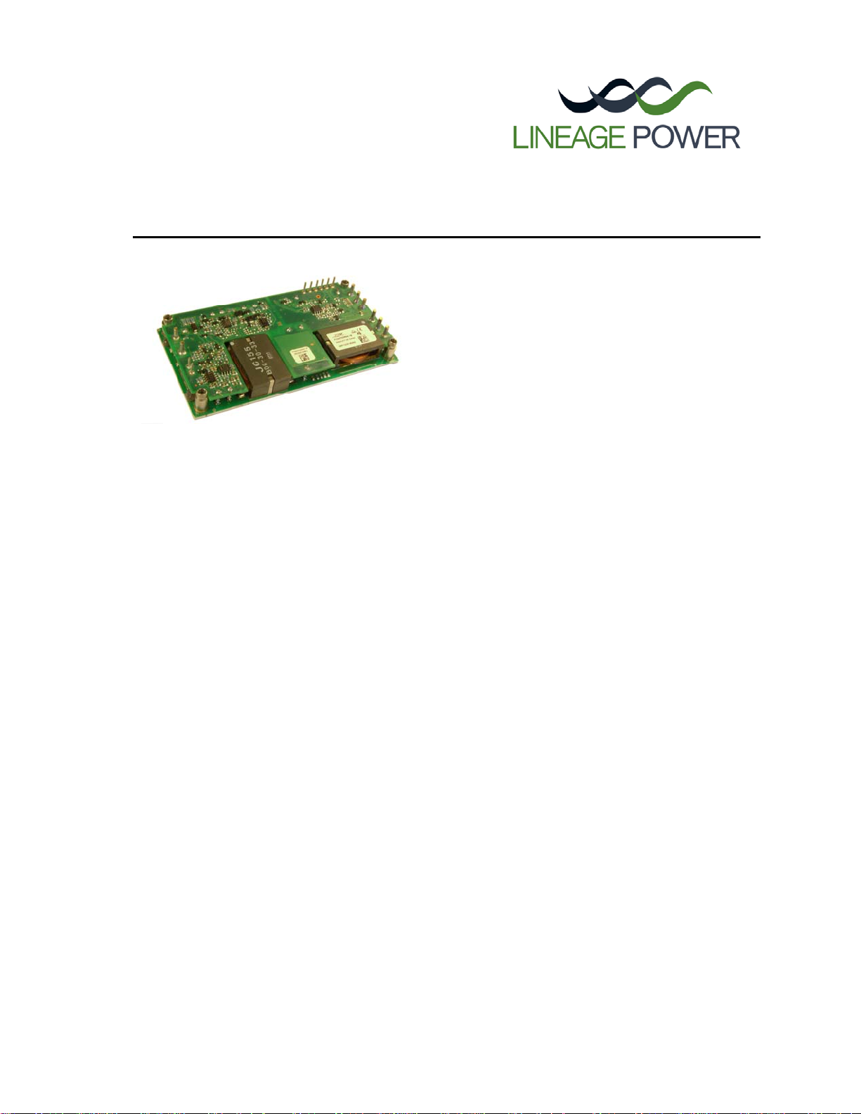
FNW500R Series Power Modules; DC-DC Converters
Applications
RF Power Amplifier
Wireless Networks
Switching Networks
Options
Output OCP/OVP auto restart
Shorter pins
Unthreaded heatsink holes
36-75 Vdc Input; 28Vdc Output; 500W Output
Features
High power density: 90 W/in3
Industry standard pin-out
Low output ripple and noise
Industry standard Full brick
116.8mm x 61.0mm x 12.7mm
(4.6” x 2.4” x 0.5”)
Remote Sense
2:1 input voltage range
Single tightly regulated output
Constant switching frequency
Latch after fault shutdown
Over temperature protection auto restart
Loosely regulated auxiliary output
Power good signal
Output voltage adjustment trim (+10%/-40%)
Wide operating case temperature range (-40°C to
100°C)
CE mark meets 73/23/EEC and 93/68/EEC
directives
UL60950-1/CSA
(
C
Licensed
ISO** 9001 and ISO 14001 certified manufacturing
facilities
§
†
CSAUS) and VDE‡ 0805:2001-12 (EN60950-1)
C22.2 No. 60950-1-03 Certified
Description
The FNW500R series of dc-dc converters are a new generation of isolated DC/DC power modules providing up to
500W output power in an industry standard full size brick footprint, which makes it an ideal choice for high voltage
and high power applications. Threaded-through holes are provided to allow easy mounting or addition of a heatsink
for high-temperature applications. The output is fully isolated from the input, allowing versatile polarity configurations
and grounding connections.
* UL is a re gistered trademark of Underwriters Laboratories, Inc.
†
CSA is a reg istered trademark of Canadian Standards Associ ation.
‡
VDE is a t rademark of Verband Deutscher Elektrotechniker e.V.
** ISO is a registered trademark of the International Orga nization of Standards
Document No: DS07-013 ver1.21
PDF name: fnw500r.ds.pdf
:
Page 2

Data Sheet
October 5, 2009
FNW500R Power Modules; DC-DC Converters
36 – 75 Vdc Input; 28Vdc Output; 500W Output
Absolute Maximum Ratings
Stresses in excess of the absolute maximum ratings can cause permanent damage to the device. These are
absolute stress ratings only, functional operation of the device is not implied at these or any other conditions in
excess of those given in the operations sections of the data sheet. Exposure to absolute maximum ratings for
extended periods can adversely affect the device reliability.
Parameter Device Symbol Min Max Unit
Input Voltage (Continuous) All V
Operating Ambient Temperature
Note: When the operating ambient temperature is within
55C~85C, the application of the module refers to the
derating curves of Figure 16.
Operating Case Temperature
(See Thermal Considerations section)
Storage Temperature All T
I/O Isolation Voltage ,Input to case All
Output to case All
All Ta
All Tc -40 100 °C
IN
stg
⎯ ⎯
⎯ ⎯
-0.3 80 Vdc
-40 85 °C
-55 125 °C
1500 Vdc
500 Vdc
Electrical Specifications
Unless otherwise indicated, specifications apply over all operating input voltage, resistive load, and temperature
conditions.
Parameter Device Symbol Min Typ Max Unit
Operating Input Voltage All VIN 36 48 75 Vdc
Maximum Input Current
(VIN=36V to 75V, IO=I
Inrush Transient All I2t 2 A2s
Input Reflected Ripple Current, peak-to-peak
(5Hz to 20MHz, 12μH source impedance; V
75V, I
= I
; see Figure 10)
O
Omax
Input Ripple Rejection (120Hz) All 50 dB
) All I
O, max
=0V to
IN
All 40 mAp-p
IN,max
CAUTION: This power module is not internally fused. An input line fuse must always be used.
This power module can be used in a wide variety of applications, ranging from simple standalone operation to being
an integrated part of complex power architecture. To preserve maximum flexibility, internal fusing is not included.
Always use an input line fuse, to achieve maximum safety and system protection. The safety agencies require a
time-delay or fast-acting fuse with a maximum rating of 30 A (see Safety Considerations section). Based on the
information provided in this data sheet on inrush energy and maximum dc input current, the same type of fuse with a
lower rating can be used. Refer to the fuse manufacturer’s data sheet for further information.
18 Adc
LINEAGE POWER 2
Page 3

Data Sheet
October 5, 2009
FNW500R Power Modules; DC-DC Converters
36 – 75 Vdc Input; 28Vdc Output; 500W Output
Electrical Specifications (continued)
Parameter Device Symbol Min Typ Max Unit
Output Voltage Set-point
(V
IN=VIN,nom
, IO=I
O, max
, Tc =25°C)
All
V
O, set
27.5 28 28.5 V
dc
Output Voltage
(Over all operating input voltage, resistive load,
and temperature conditions until end of life)
All
V
O
27.15
⎯
28.85 V
dc
Output Regulation
Line (VIN=V
Load (IO=I
Temperature (Tc = -40ºC to +100ºC) All
IN, min
O, min
to V
to I
) All ⎯ 0.05 0.2 %Vo
IN, max
) All ⎯ 0.05 0.2 %Vo
O, max
⎯
100 300 mV
Output Ripple and Noise on nominal output
(VIN=V
RMS (5Hz to 20MHz bandwidth) All
Peak-to-Peak (5Hz to 20MHz bandwidth) All
IN, nom
and IO=I
O, min
to I
)
O, max
⎯ ⎯
⎯
140 300 mV
80 mV
rms
pk-pk
External Capacitance
Note: use a minimum 470uF output capacitor. If
the ambient temperature is less than -20
o
C, use
All C
O, max
470 1000 5000 μF
more than 3 of recommended minimum
capacitors.
Output Current All I
Output Current Limit Inception All I
Efficiency
V
IN=VIN, nom
I
O=IO, max , VO
, Tc=25°C
= V
O,set
All
Switching Frequency f
o
O, lim
η
sw
1.8 18 Adc
19 22 25.2 Adc
⎯
⎯
91
300
⎯
⎯
%
kHz
Dynamic Load Response
(ΔIo/Δt=1A/10μs; Vin=Vin,nom; Tc=25°C;
Tested with a 470 μF aluminum and a 10 µF
ceramic capacitor across the load.)
Load Change from Io= 50% to 75% of Io,max:
Peak Deviation
Settling Time (Vo<10% peak deviation)
Load Change from Io= 25% to 50% of Io,max:
Peak Deviation
Settling Time (Vo<10% peak deviation)
All
V
t
V
pk
ts
__ 3 __ %V
pk
s
⎯
__
⎯
3
2
2
⎯
__
⎯
%V
ms
ms
O, set
O, set
Isolation Specifications
Parameter Symbol Min Typ Max Unit
Isolation Capacitance C
Isolation Resistance R
iso
iso
⎯
10
1500
⎯ ⎯
⎯
pF
MΩ
General Specifications
Parameter Device Symbol Min Typ Max Unit
Calculated Reliability based upon Telcordia SR332 Issue 2: Method
=40°C, airflow = 200 lfm, 90% confidence)
T
A
I Case 3 (I
=80%I
O
O, max
,
All
Weight All
LINEAGE POWER 3
FIT 402 109/Hours
MTBF 2,487,326 Hours
⎯
150
⎯
g
5.3 oz.
Page 4

Data Sheet
p
October 5, 2009
FNW500R Power Modules; DC-DC Converters
36 – 75 Vdc Input; 28Vdc Output; 500W Output
Feature Specifications
Unless otherwise indicated, specifications apply over all operating input voltage, resistive load, and temperature
conditions. See Feature Descriptions for additional information.
Parameter Device Symbol Min Typ Max Unit
Remote On/Off Signal Interface
(VIN=V
Refer to remote on/off descri
Remote On/Off Current – Logic ON All I
Remote On/Off Current – Logic OFF All I
Turn-On Delay and Rise Times
(Vin=Vin,nom, IO=I
Case1: T
application of Vin with Remote On/Off set to ON,
IN, min
to V
delay
; open collector or equivalent),
IN, max
O, max
tion and Figure 11.
, 25C)
= Time until VO = 10% of Vo,set from
All
on/off
on/off
T
60 75 100 ms
delay
1.0
⎯ ⎯
⎯
5.0 mA
50 μA
Case2: T
application of Remote On/Off from Off to On with Vin
already applied for at least one second.
T
rise
of V
O,set
= Time until VO = 10% of Vo,set from
delay
= time for VO to rise from 10% of V
.
O,set
to 90%
All
All
T
T
delay
rise
⎯
⎯
5
25
⎯
⎯
Output Voltage Overshoot 3 % V
(IO=80% of I
Output Voltage Adjustment
(See Feature Descriptions):
Output Voltage Remote-sense Range
(only for No Trim or Trim down application )
Output Voltage Set-point Adjustment Range (trim) All V
Output Overvoltage Protection
Over Temperature Protection
(See Feature Descriptions)
Input Under Voltage Lockout V
Input Over voltage Lockout V
, TA=25°C)
O, max
Turn-on Threshold
Turn-off Threshold
Hysteresis
Turn-on Threshold
Turn-off Threshold
Hysteresis
All V
All
V
All T
All
All
All
All
All
All
sense
60
trim
O, limit
ref
IN, UVLO
IN, OVLO
__
32
⎯
35 36 V
30 31 V
4 V
⎯
79 80
--- 4 --- V
__
__
⎯
106
2 %V
110 %V
38 V
⎯
76 78 V
⎯
ms
ms
o,nom
o,nom
°C
V
O, set
LINEAGE POWER 4
Page 5
Data Sheet
October 5, 2009
FNW500R Power Modules; DC-DC Converters
36 – 75 Vdc Input; 28Vdc Output; 500W Output
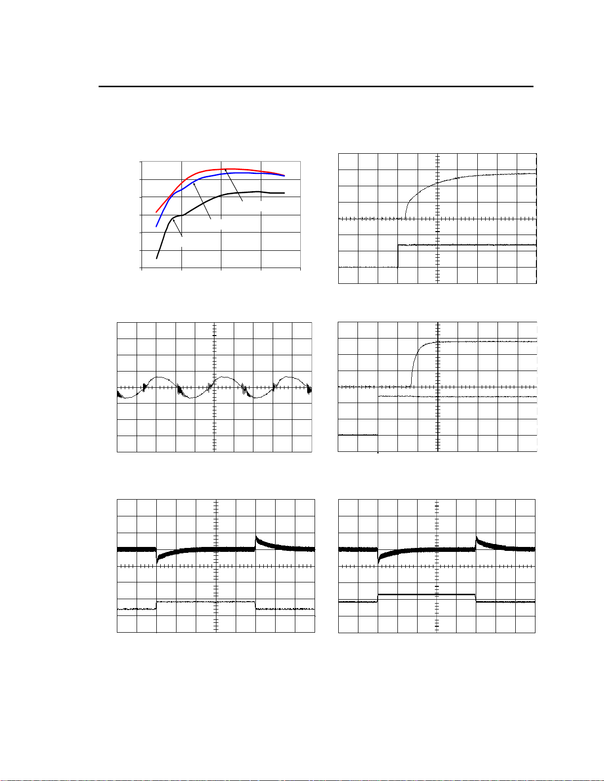
Characteristic Curves
The following figures provide typical characteristics for the FNW500R (28V, 18A) at 25ºC. The figures are identical for
either positive or negative Remote On/Off logic.
93.0
91.0
89.0
Vin=36V
87.0
85.0
Vin=48V
Vin=75V
83.0
EFFICIENCY (%)
81.0
0 5 10 15 20
OUTPUT CURRENT, Io (A)
Figure 1. Converter Efficiency versus Output
Current.
(V) (100mV/div)
O
V
OUTPUT VOLTAGE,
TIME, t (1μs/div)
Figure 2. Typical Output Ripple and Noise at Room
Temperature and 48Vin; I
o
= I
o,max
; C
= 470µF.
o,ext
(V) (10V/div)
O
(V) (2V/div) V
ON/OFF
V
On/Off VOLTAGE OUTPUT VOLTAGE
TIME, t (10ms/div)
Figure 4. Typical Start-Up Using Remote On/Off,
R1=30Kohm; C
(V) (10V/div)
O
INPUT VOLTAGE OUTPUT VOLTAGE
Vin (V) (20V/div) V
Figure 5. Typical Start-Up Using from V
logic version shown; C
= 470µF.
o,ext
TIME, t (50ms/div)
= 470µF.
o,ext
, positive
IN
(V) (500mV/div)
O
(A) (10A/div) V
O
VOLTAGE
I
TIME, t (1ms/div)
Figure 3. Transient Response to Dynamic Load
Change from 25% to 50% to 25% of Full Load at
Room Temperature and 48 Vdc Input; 0.1A/uS
5
(V) (500mV/div)
O
(A) (5A/div) V
O
I
OUTPUT CURRENT OUTPUT VOLTAGE
TIME, t (1ms/div)
Figure 6. Transient Response to Dyna mic Load
Change from 50% to 75% to 50% of Full Load at
Room Temperature and 48 Vdc Input; 0.1A/uS
Page 6

Data Sheet
October 5, 2009
FNW500R Power Modules; DC-DC Converters
36 – 75 Vdc Input; 28Vdc Output; 500W Output
Test Configurations
Note: Measure the input reflected-ripple current with a
simulated source inductance (LTEST) of 12 µH. Capacitor CS
offsets possible battery impedance. Measure the current, as
shown above.
Figure 7. Input Reflected Ripple Current Test Setup.
Note: Use a Cout (470 µF Low ESR aluminum or tantalum
capacitor typical), a 0.1 µF ceramic capacitor and a 10 µF
ceramic capacitor, and Scope measurement should be made
using a BNC socket. Position the load between 51 mm and 76
mm (2 in. and 3 in.) from the module.
Figure 8. Output Ripple and Noise Test Setup.
Note: All measurements are taken at the module terminals.
When socketing, place Kelvin connections at module terminals
to avoid measurement errors due to socket contact resistance.
Figure 9. Output Voltage and Efficiency Tes t Setup.
Design Considerations
Input Source Impedance
The power module should be connected to a low
ac-impedance source. A highly inductive source
impedance can affect the stability of the power module.
For the test configuration in Figure 7, a 470μF Low
ESR aluminum capacitor, C
power module helps ensure the stability of the unit.
Consult the factory for further application guidelines
, mounted close to the
IN
Output Capacitance
The FNW500R power module requires a minimum
output capacitance of 470µF Low ESR aluminum
capacitor, C
range of load and line conditions, see Figure 8. If the
ambient temperature is under -20C, it is required to use
at least 3 pcs of minimum capacitors in parallel. In
general, the process of determining the acceptable
values of output capacitance and ESR is complex and
is load-dependant.
to ensure stable operation over the full
out
Safety Considerations
For safety-agency approval of the system in which the
power module is used, the power module must be
installed in compliance with the spacing and separation
requirements of the end-use safety agency standard,
i.e., UL60950-1, CSA C22.2 No. 60950-1-03,
EN60950-1 and VDE 0805:2001-12.
For end products connected to –48V dc, or –60Vdc
nominal DC MAINS (i.e. central office dc battery plant),
no further fault testing is required. *Note: -60V dc
nominal battery plants are not available in the U.S. or
Canada.
For all input voltages, other than DC MAINS, where the
input voltage is less than 60V dc, if the input meets all
of the requirements for SELV, then:
The output may be considered SELV. Output
voltages will remain within SELV limits even with
internally-generated non-SELV voltages. Single
component failure and fault tests were performed
in the power converters.
One pole of the input and one pole of the output
are to be grounded, or both circuits are to be kept
floating, to maintain the output voltage to ground
voltage within ELV or SELV limits. However, SELV
will not be maintained if V
grounded simultaneously.
(+) and VO(+) are
I
LINEAGE POWER 6
Page 7

Data Sheet
October 5, 2009
FNW500R Power Modules; DC-DC Converters
36 – 75 Vdc Input; 28Vdc Output; 500W Output
Safety Considerations (continued)
For all input sources, other than DC MAINS, where the
input voltage is between 60 and 75V dc (Classified as
TNV-2 in Europe), the following must be meet, if the
converter’s output is to be evaluated for SELV:
The input source is to be provided with reinforced
insulation from any hazardous voltage, including
the ac mains.
One Vi pin and one Vo pin are to be reliably
earthed, or both the input and output pins are to be
kept floating.
Another SELV reliability test is conducted on the
whole system, as required by the safety agencies,
on the combination of supply source and the
subject module to verify that under a single fault,
hazardous voltages do not appear at the module’s
output.
All flammable materials used in the manufacturing of
these modules are rated 94V-0, or tested to the
UL60950 A.2 for reduced thickness.
The input to these units is to be provided with a
maximum 30 A fast-acting or time-delay fuse in the
unearthed lead.
Feature Description
Remote On/Off
Remote ON/OFF control is available as standard and
has positive logic remote On/Off mode only. The
converter will be active as long as a current Ion/off (1 to
5mA) is flowing into the ON/OFF+ (pin 4) and from the
ON/OFF- (pin 3), and inactive when no current is
flowing. Remote control pins are isolated up to 1.5 kV.
The voltage to drive this current can be derived from
the input voltage, the output voltage, or an external
supply with an appropriate current limit resistor. The
maximum forward current allowable without damage is
5 mA, and the maximum reverse current is 10mA. A
typical remote ON/OFF circuit is shown as Figure 10.
The current limit resistor (R1) is connected from Vin (+)
pin to ON/OFF + pin, an open collector or an equivalent
switch can be connected between ON/OFF - and V
pins to control ON/OFF operation. A 0 Ohm resistor
(R2) can be used if no open collector or switch used.
For 48Vin, an appropriate R1 value is recommended to
be 30Kohm (0.5W).
(-)
I
Figure 10. Circuit configuration for using Remote
On/Off Implementation.
Overcurrent Protection
To provide protection in a fault output overload
condition, the module is equipped with internal currentlimiting circuitry and can endure current limit for few
milli-seconds. A latching shutdown option is standard. If
overcurrent persists for few milli-seconds, the module
will shut down and remain off until the module is reset
by either cycling the input power or by toggling the
on/off pin for one second.
An auto-restart option (4) is also available in a case
where an auto recovery is required. If overcurrent
persists for few milli-seconds, the module will shut
down and auto restart until the fault condition is
corrected. If the output overload condition still exists
when the module restarts, it will shut down again. This
operation will continue indefinitely, until the overcurrent
condition is corrected.
Over Voltage Protection
The output overvoltage protection consists of circuitry
that monitors the voltage on the output terminals. If the
voltage on the output terminals exceeds the over
voltage protection threshold, then the module will
shutdown and latch off. The overvoltage latch is reset
by either cycling the input power for one second or by
toggling the on/off signal for one second. The
protection mechanism is such that the unit can continue
in this condition until the fault is cleared.
An auto-restart option (4) is also available in a case
where an auto recovery is required.
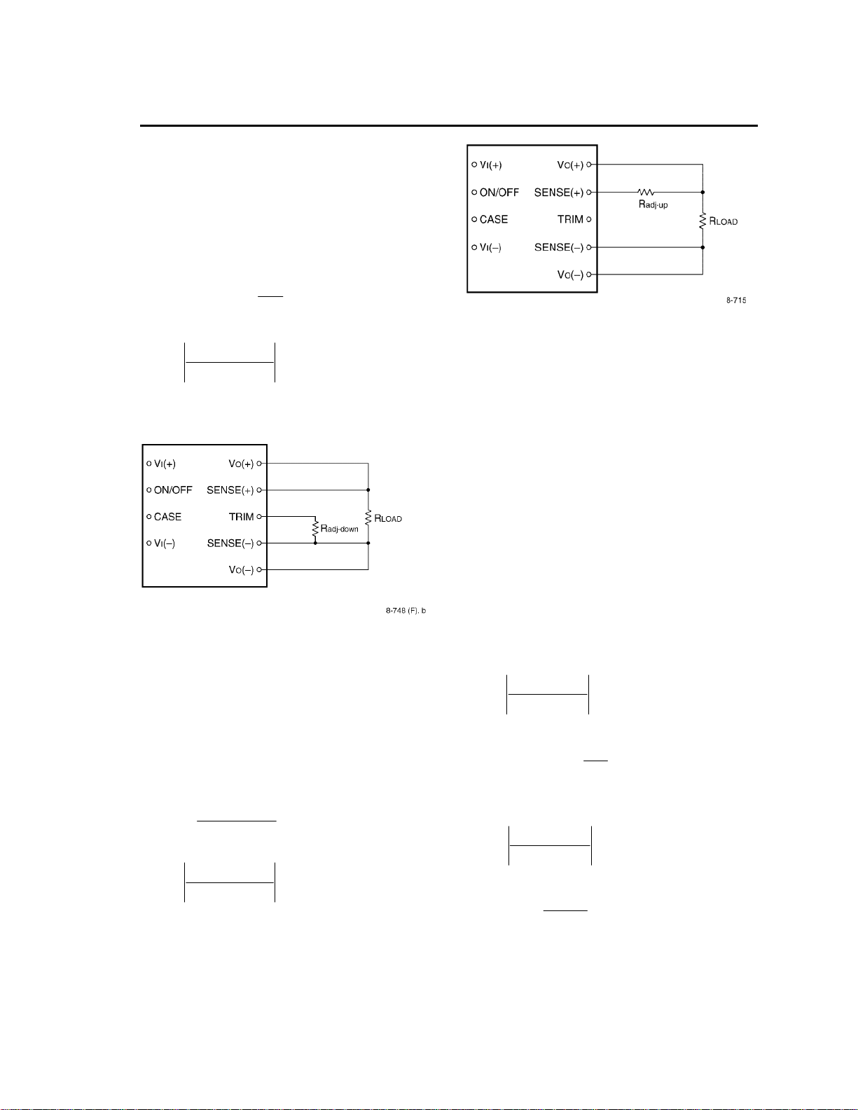
Output Voltage Programming
Trimming allows the user to increase or decrease the
output voltage set point of a module. Trimming down is
accomplished by connecting an external resistor
between the TRIM pin and the SENSE(-) pin. Trimming
up is accomplished by connecting external resistor
between the SENSE(+) pin and Vo(+) pin. The trim
resistor should be positioned close to the module.
Be sure to use a zero resistor or short SENSE(+) and
Vo(+) pins when the trim up function is not used.
If not using the trim down feature, leave the TRIM pin
open.
LINEAGE POWER 7
Page 8
Data Sheet
×
October 5, 2009
FNW500R Power Modules; DC-DC Converters
36 – 75 Vdc Input; 28Vdc Output; 500W Output
Feature Description (continued)
With an external resistor between the TRIM and
SENSE(-) pins (Radj-down), the output voltage set
point (Vo,adj) decreases (see Figure 11). The following
equation determines the required external-resistor
value to obtain a percentage output voltage change of
Δ%.
For output voltages: 28V
100
− KR downadj 1
Where,
,
=Δ
V
= Desired output voltage set point (V).
desired
Figure 11. Circuit Configuration to Dec reas e Outpu t
Voltage.
⎛
97.5
×=
⎜
Δ
⎝
desirednomo
VV
−
,
nomo
V
Trim Up – Increase Output Voltage
With an external resistor connected between the Vo(+)
and SENSE(+) pins
Vo,adj) increases (see Figure 12).
point (
The following equation determines the required
external-resistor value to obtain a percentage output
voltage change of Δ%.
For output voltages: 28V
R upadj
Where,
=− K
=Δ
V
= Desired output voltage set point (V).
desired
(Radj-up), the output voltage set
Δ×
nomVo
100
VV
−
,
nomodesired
,
nomo
V
⎞
Ω
−
⎟
%
⎠
100%
×
%,
Ω
100%
×
Figure 12. Circuit Configuration to Increase Output
Voltage.
The voltage between the Vo(+) and Vo(-) terminals
must not exceed the minimum output overvoltage shutdown value indicated in the Feature Specifications
table. This limit includes any increase in voltage due to
remote- sense compensation and output voltage setpoint adjustment (trim). See Figure 13.
Although the output voltage can be increased by both
the remote sense and by the trim, the maximum
increase for the output voltage is not the sum of both.
The maximum increase is the larger of either the
remote sense or the trim.
The amount of power delivered by the module is
defined as the voltage at the output terminals multiplied
by the output current. When using remote sense and
trim, the output voltage of the module can be
increased, which the same output current would
increase the power output of the module. Care should
be taken to ensure that the maximum output power of
the module remains at or below the maximum rated
F
power.
Examples:
To trim down the output of a nominal 28V module to
16.8V
VV
8.1628
% ×
=Δ
∆% = 40
−
V
28
100
⎛
97.5
⎜
⎝
= 8.96 kΩ
R
adj-down
To trim up the output of a nominal 28V module to 30.8V
288.30
−
% ×
=Δ
Δ% = 10
=− KupRadj
28
VV
V
1028
40
100
−×=− KR downadj 1
100
Ω
⎞
Ω
⎟
⎠
100
R
= 2.8 KΩ
tadj-up
LINEAGE POWER 8
Page 9

Data Sheet
October 5, 2009
FNW500R Power Modules; DC-DC Converters
36 – 75 Vdc Input; 28Vdc Output; 500W Output
Feature Description (continued)
Remote sense
Remote sense minimizes the effects of distribution
losses by regulating the voltage at the remote-sense
connections (see Figure 13). For No Trim or Trim down
application, the voltage between the remote-sense pins
and the output terminals must not exceed the output
voltage sense range given in the Feature Specifications
table i.e.:
[Vo(+) – Vo(-)] – [SENSE(+) – SENSE(-)] ≤ 2% of
V
.
o,nom
The voltage between the Vo(+) and Vo(-) terminals
must not exceed the minimum output overvoltage shutdown value indicated in the Feature Specifications
table. This limit includes any increase in voltage due to
remote-sense compensation and output voltage setpoint adjustment (trim). See Figure 13. If not using the
remote-sense feature to regulate the output at the point
of load, then connect SENSE(+) to Vo(+) and SENSE() to Vo(-) at the module.
Although the output voltage can be increased by both
the remote sense and by the trim, the maximum
increase for the output voltage is not the sum of both.
The maximum increase is the larger of either the
remote sense or the trim. The amount of power
delivered by the module is defined as the voltage at the
output terminals multiplied by the output current. When
using remote sense and trim: the output voltage of the
module can be increased, which at the same output
current would increase the power output of the module.
Care should be taken to ensure that the maximum
output power of the module remains at or below the
maximum rated power.
approximately 20 ºC the converter will automatically
restart.
The module can be restarted by cycling the dc input
power for at least one second or by toggling the remote
on/off signal for at least one second.
Auxiliary Power Output
The module has an auxiliary power output, available on
pin 16, referenced to the Sense- pin. The output is
derived from the internal secondary bias supply and is
capable of delivering up to 15 mA, with a voltage range
that varies between 9V
typically used to drive LEDs. To prevent internal
module damage, do not connect or short this pin to any
other pin on the module.
and 13 Vdc. This supply is
dc
Power Good Signal
The module contains a power good signal on pin 15,
consisting of an open collector circuit that is referenced
to the Sense- pin on the secondary side of the module.
The power good signal is active low, when the module
is operating normally. The maximum current that can
sunk at this pin, during normal operation active low, is
35 mA
during module abnormal operation active high, is 35V
During transient load changes or during overcurrent
hiccup events, the sanity of the power good signal is
not guaranteed.
, and the maximum voltage allowed on the pin,
dc
dc
.
Figure 13. Effective Circuit Configuration for SingleModule Remote-Sense Operation Output Voltage.
Over Temperature Protection
The FNW500R module provides with non-latching over
temperature protection. A temperature sensor monitors
the operating temperature of the converter. If the
reference temperature exceeds a threshold of 106 °C
(typical) at the center of the baseplate, the converter
will shut down and disable the output. When the
baseplate temperature has decreased by
LINEAGE POWER 9
Page 10

Data Sheet
(C)
October 5, 2009
FNW500R Power Modules; DC-DC Converters
36 – 75 Vdc Input; 28Vdc Output; 500W Output
Thermal Considerations
The power modules operate in a variety of thermal
environments; however, sufficient cooling should be
provided to help ensure reliable operation of the unit.
Heat-dissipating components inside the unit are
thermally coupled to the case. Heat is removed by
conduction, convection, and radiation to the
surrounding environment. Proper cooling can be
verified by measuring the case temperature. Peak
temperature (T
) occurs at the position indicated in
C
Figure 14.
Considerations include ambient temperature, airflow,
module power dissipation, and the need for increased
reliability. A reduction in the operating temperature of
the module will result in an increase in reliability. The
thermal data presented here is based on physical
measurements taken in a wind tunnel.
For reliable operation this temperature should not
exceed 100ºC.
23mm
Figure 14. Case (T
Location (top view).
The output power of the module should not exceed the
rated power for the module as listed in the ordering
Information table.
Although the maximum T
modules is 100°C, you can limit this temperature to a
lower value for extremely high reliability.
Thermal Derating
The curve in Figure 15 depicts the temperature/output
power derating curve for conduction cooling type
applications. These applications typically will provide a
low thermal impedance cooling interface that is
attached to the top surface of the module and is
maintained at or below the T
air surrounding the module is still and is held below
72°C. The module will deliver full power when the case
(T
) Temperature Measurement Location is maintained
C
at or below 95°C. For temperatures above 95°C, the
output current must be limited by the derating curve.
For other applications, such as force air cooling, the
FNW500R power module has large power dissipation,
a customized heatsink is required for application.
TOP VIEW
45mm
) Temperature Measurement
c
temperature of the power
c
temperature. The internal
C
600
500
400
300
200
100
Output Po wer (W @ Vou t=28 V)
0
60 65 70 75 80 85 90 95 100
Tcase
Figure 15. Output Power Derating for FNW500R in
Conduction cooling (cold plate) applications;
T
<72ºC in vicinity of module interior; VIN = V
a
IN, NOM
Layout Considerations
The FNW500R power module series are aluminum
base board packaged style, as such; component
clearance between the bottom of the power module
and the mounting (Host) board is limited. Avoid placing
copper areas on the outer layer directly underneath the
power module.
Post Solder Cleaning and Drying
Considerations
Post solder cleaning is usually the final circuit-board
assembly process prior to electrical board testing. The
result of inadequate cleaning and drying can affect both
the reliability of a power module and the testability of
the finished circuit-board assembly. For guidance on
appropriate soldering, cleaning and drying procedures,
refer to Lineage Power Board Mounted Power
Modules: Soldering and Cleaning Application Note.
LINEAGE POWER 10
Page 11

Data Sheet
October 5, 2009
FNW500R Power Modules; DC-DC Converters
36 – 75 Vdc Input; 28Vdc Output; 500W Output
Mechanical Outline for Through-Hole Module
Dimensions are in millimeters and [inches].
Tolerances: x.x mm ± 0.5 mm [x.xx in. ± 0.02 in.] (Unless otherwise indicated)
x.xx mm ± 0.25 mm [x.xxx in ± 0.010 in.]
TOP VIEW
SIDE VIEW
BOTTOM
VIEW
Pin Description Pin Description Pin Description Pin Description
1 Vin – 5 Vo+ 9 Vo- 13 Trim
2 Vin + 6 Vo+ 10 Vo- 14 N/A
3 - On/Off 7 Vo+ 11 Sense (-) 15
4 +On/Off 8 Vo- 12 Sense (+) 16
LINEAGE POWER 11
Power Good
Aux Power
Page 12

Data Sheet
October 5, 2009
FNW500R Power Modules; DC-DC Converters
36 – 75 Vdc Input; 28Vdc Output; 500W Output
Recommended Pad Layout for Through Hole Module
Dimensions are in millimeters and [inches].
Tolerances: x.x mm ± 0.5 mm [x.xx in. ± 0.02 in.] (Unless otherwise indicated)
x.xx mm ± 0.25 mm [x.xxx in ± 0.010 in.]
LINEAGE POWER 12
Page 13

Data Sheet
a
©
October 5, 2009
FNW500R Power Modules; DC-DC Converters
36 – 75 Vdc Input; 28Vdc Output; 500W Output
Ordering Information
Please contact your Lineage Power Sales Representative for pricing, availability and optional features.
Table 2. Device Code
Input Voltage
Output
Voltage
48V (36-75Vdc) 28V 18A 91% Through hole FNW500R4 CC109141223
48V (36-75Vdc) 28V 18A 91% Through hole FNW500R64-18 CC109141388
Table 3. Device Options
Option Device Code Suf f i x
Auto restart (hiccup) protection 4
Pin Length: 3.68 mm ± 0.25mm , (0.145 in. ± 0.010 in.) 6
Unthreaded heatsink mounting holes 18
Output
Current
Efficiency Connector
Type
Product codes Comcodes
World Wide Headquarters
Lineage Power Corporation
601 Shil oh Roa d, Plano, TX 75074, USA
+1-800-526-7819
(Outsi de U.S.A.: +1-972-244-9428)
www.lineagepower.com
e-mail: techsupport1@lineagepower.com
Linea ge Power res erves th e right to make change s to the prod uct(s) or i nformation c ontained herein without not ice. No l iability is assumed as a result o f their use o r
pplication . No righ ts under any patent accompany the sal e of any s uch produc t(s) or informati on.
Linea ge Power D C-DC pro ducts are p rotected unde r v arious pa tents. Information on these patents is availabl e at www.line agepower.com/paten ts.
2009 Line age Power Corporation, (Plan o, Texas) All Inte rn ational Rights Reserved.
Asia-Pacific Headquarters
Tel: + 65 6593 7211
Europe, Middle-East and Africa Headquarters
Tel: + 49 898 780 672 80
India Headquarters
Tel: + 91 80 2841163 3
Document No: DS07-013 ver1.21
PDF name: fnw500r.ds.pdf
 Loading...