

Page 1
Data Sheet
October 2009
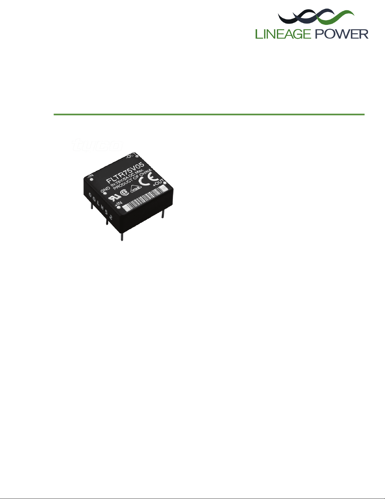
FLTR75V05 Filter Module
75 Vdc Input Maximum, 5 A Maximum
Features
RoHS Compliant
Applications
n
Common-mode and differential-mode filtering of
power supply dc input and output lines
n
Distributed power architectures
n
Telecom
n
Datacom
n
Compatible with RoHS EU Directive 200295/EC
n
Compatible in Pb- free or SnPb reflow environment
n
Small size: 25.4 mm x 25.4 mm x 10.2 mm
(1.0 in. x 1.0 in. x 0.4 in.)
n
Optimized for use with high-frequency switching
dc-to-dc power modules
n
Printed-circuit board mountable
n
Operating case temperature range:
–40 °C to +100 °C
Options
n
Choice of pin lengths
Description
The FLTR75V05 Filter Module is designed to reduce the conducted common-mode and differential-mode noise
on input or output lines of high-frequency switching power supplies. The module has a maximum current rating
of 5 A. It provides high insertion loss throughout the frequency range regulated by the U.S. Federal Communications Commission (FCC) and the International Special Committee on Radio Interference (CISPR) for conducted emissions.
The module is 25.4 mm long, 25.4 mm wide, and 10.2 mm high (1.0 in. x 1.0 in. x 0.4 in.) and mounts on a PC
board in a natural convection or forced-air environment.
Page 2
FLTR75V05 Filter Module
75 Vdc Input Maximum, 5 A Maximum
Data Sheet
October 2009
Introduction
High-density power modules are usually designed to operate at a high switching frequency to reduce the size of
the internal filter components. The small EMI filters internal to the modules are often inadequate to meet stringent
international EMI requirements. Many high-density electronic packaging techniques can increase the noise conducted onto the modules’ input and output lines. For example, the close proximity of switching components to the
input pins increases internal noise coupling; and planar transformers, designed to handle high-power levels in lowprofile packages, have high interwinding capacitance that can increase common-mode current levels. Also, metal
substrates used to facilitate heat transfer from the power train components to an external heat sink add to common-mode noise because of the large capacitance between switching components and the metal substrate.
Many international agencies specify conducted and radiated emissions limits for electronic products. Included
among these are CISPR, FCC, VCCI, and the new CE specifications. Most agency-conducted noise limits apply
only to noise currents induced onto the ac power lines in finished products. European Telecommunication Standard
Instructions (ETSI) are an exception, applying CE requirements to dc supplies with cables over three meters long.
Although not required to do so by agency standards, some system designers apply the conducted emissions
requirements to subassemblies within the product to reduce internal interference between subsystems and to
reduce the difficulty of meeting overall system requirements.
To meet these requirements, external filtering of the power module is often required. When used in conjunction with
the recommended external components and layout, the Lineage Power filter module will significantly reduce the
conducted differential and common-mode noise returned to the power source. CISPR and FCC class B requirements can be met by using the filter as described in the following sections.
Absolute Maximum Ratings
Stresses in excess of the absolute maximum ratings can cause permanent damage to the device. These are absolute stress ratings only. Functional operation of the device is not implied at these or any other conditions in excess
of those given in the operations sections of the data sheet. Exposure to absolute maximum ratings for extended
periods can adversely affect device reliability.
Parameter Symbol Min Max Unit
Input Voltage:
Continuous
Transient (100 ms)
Voltage from GND to Either Input Lead — — 1500 Vdc
Operating Case Temperature T
Storage Temperature T
I
V
VI, trans
C –40 100 °C
stg –55 125 °C
—
—
75
100
Vdc
V
2 Lineage Power
Page 3
Data Sheet
October 2009
75 Vdc Input Maximum, 5 A Maximum
FLTR75V05 Filter Module
Electrical Specifications
Unless otherwise indicated, specifications apply over all operating input voltage and temperature conditions.
Parameter Symbol Min Typ Max Unit
Resistance per Leg R — — 20 mΩ
Maximum Average Current
(T
A = 60 °C, 2.03 m/s (400 lfm) air)
Maximum Average Current
A = 60 °C, natural convection)
(T
Common-mode Insertion Loss
(50 Ω circuit, 500 kHz)
Differential-mode Insertion Loss
(50 Ω circuit, 500 kHz)
I
max —— 5 A
I
max ——3.3A
——28—dB
——25—dB
Lineage Power 3
Page 4
FLTR75V05 Filter Module
6
75 Vdc Input Maximum, 5 A Maximum
Data Sheet
October 2009
Characteristics
30
0 m/s (0 ft./min.)
20
10
RISE, ΔT (˚C)
TEMPERATURE
0
12345
Figure 1. Typical Case Temperature Rise vs.
0
-10
-20
-30
-40
-50
-60
COMMON MODE
-70
INSERTION LOSS (dB)
-80
10E+3 100E+3 1E+6 10E+6 100E+6
1.0 m/s (200 ft./min.)
2.0 m/s (400 ft./min.)
CURRENT (A)
Average Current (Case Temperature
Must Be Kept Below 100 °C)
FREQUENCY (Hz)
1-0352
20
10
0
-10
-20
-30
-40
-50
-60
DIFFERENTIAL MODE
INSERTION LOSS (dB)
-70
10E+3 100E+3 1E+6 10E+6 100E+
FREQUENCY (Hz)
1-0319
Figure 3. Typical Differential-Mode Insertion Loss
in a 50 Ω Circuit
Internal Schematics
IN
GND
OUT
8-1324 (F).b
1-0320
Figure 4. Internal Schematic
Figure 2. Typical Common-Mode Insertion Loss in
a 50 Ω Circuit
44 Lineage Power
Page 5

Data Sheet
October 2
FLTR75V05 Filter Module
75 Vdc Input Maximum, 5 A Maximum
Application
Conducted noise on the input power lines can occur as
either differential-mode or common-mode noise currents. Differential-mode noise is measured between the
two input lines, and is found mostly at the lowfrequency end of the spectrum. This noise shows up as
noise at the fundamental switching frequency and its
harmonics. Common-mode noise is measured
between the input lines and ground and is mostly
broadband noise above 10 MHz. The high-frequency
nature of common-mode noise is mostly due to the
high-speed switching transitions of power train components. Either or both types of noise may be covered in
a specification, as well as a combination of the two. An
approved measurement technique is often described,
as well.
Differential-mode noise is best attenuated using a filter
composed of line-to-line capacitors (X caps) and series
inductance, provided by either a discrete inductor or
the leakage inductance of a common-mode choke. In
addition to the differential filtering provided by the filter
module, it is recommended that an electrolytic capacitor be located at the converter side of the filter to provide additional attenuation of low-frequency differential
noise and to provide a low source impedance for the
converter, preventing input filter oscillations and loadtransient induced input voltage dips.
Common-mode noise is best attenuated by capacitors
from power module input to power module output,
capacitors from each input line to a shield plane
(Y caps), and common-mode chokes. It is recommended that ceramic capacitors be added around each
power module from each input and output pin to a
shield plane under the module. The shield plane should
be connected to the CASE pin.
The GND pin of the filter module is attached to Y caps
within the module. This pin should be tied to a quiet
chassis ground point away from the power modules.
GND of the filter module should not be tied to the
CASE pin of the power module since this is a noisy
node and will inject noise into the filter, increasing the
input common-mode noise.
If no quiet grounding point is available, it is best to
leave the filter module GND pin unattached. Each
power system design will be different, and some experimentation may be necessary to arrive at the best configuration.
Figure 5 shows a typical schematic of a power module
with filter module and recommended external components. Figure 6 is a proposed layout. More than one
power module may be attached to a single filter module
as long as input current does not exceed 5 A. Figure 7
shows the recommended schematic for two power
modules attached to a single filter.
In applications where the addition of input to output
capacitors is undesirable, do not use C3 and C4 shown
in Figures 5 and 6, and do not use C3, C4, C8, and C9
shown in Figure 7.
In –48 V applications where the shield plane and the
power module case must be tied to a signal, remove
C1 in Figures 5 and 6, remove C1 and C6 in Figure 7,
and connect the shield plane and CASE pin to the V
plane.
In +48 V applications where the shield plane and the
power module case must be tied to a signal, remove
C2 in Figures 5 and 6, remove C2 and C7 in Figure 7,
and connect the shield plane and CASE pin to the V
plane.
I(+)
I(–)
Lineage Power 5
Page 6

FLTR75V05 Filter Module
75 Vdc Input Maximum, 5 A Maximum
Application (continued)
Data Sheet
October 2009
SHIELD PLANE
C1
Vdc INPUT(–)
CHASSIS GROUND
Vdc INPUT(+)
Note: C1 through C4 can be 0.01 µF to 0.1 µF. Select the voltage rating to meet input-to-output isolation requirements. C5 should be the
recommended value indicated in the power module data sheet.
VI(–)
GND
VI(+)
MODULE
FILTER
V
V
O(–)
C5
O(+)
VI(–)
V
I(+)
C2
CASE
POWER MODULE
C3 C4
O(–)
V
V
O(+)
8-1325 (F).b
Figure 5. Recommended Schematic When Used as the Input Filter to a High-Frequency dc-to-dc Converter
C1
POWER
MODULE
C4
FILTER
MODULE
V
I(+)
Vdc INPUT(+)
Vdc INPUT(–)
CHASSIS
GROUND
Note: Vdc input(+) and Vdc input(–) planes should overlay each other, as should the VI(+) and VI(–) planes, as should the VO(+) and VO(–)
planes. Avoid routing signals or planes under the power module or the filter module. Ensure all connections are low impedance.
C5
I(–)
V
CASE
C2
SHIELD
PLANE
C3
V
O(+)
V
O(–)
1-0118
Figure 6. Recommended Layout When Used as the Input Filter to a High-Frequency dc-to-dc Converter
6 Lineage Power
Page 7

Data Sheet
October 2009
Application (continued)
FLTR75V05 Filter Module
75 Vdc Input Maximum, 5 A Maximum
SHIELD PLANE
C6
C1
VI2(–)
I2(+)
V
V
I1(–)
C7
CASE 2
POWER MODULE 2
SHIELD PLANE
C2
CASE 1
C8 C9
V
O2(–)
O2(+)
V
C3 C4
V
O1(–)
Vdc INPUT(–)
CHASSIS GROUND
Vdc INPUT(+)
Note: C1 through C4 and C6 through C9 can be 0.01 µF to 0.1 µF. Select the voltage rating to meet input-to-output isolation requirements.
C5 should be the recommended value indicated in the power module data sheet.
V
I(–)
GND
I(+)
V
MODULE
FILTER
V
O(–)
VO(+)
C5
VI1(+)
POWER MODULE 1
V
O1(+)
8-1362 (F).a
Figure 7. Recommended Schematic of Filter Module with Two Power Modules
Lineage Power 7
Page 8
FLTR75V05 Filter Module
75 Vdc Input Maximum, 5 A Maximum
Data Sheet
October 2009
Application (continued)
Figures 9, 10 & 11 show some experimental results for
various Lineage Power modules obtained by using the filter module, together with the recommended external
components shown in Figures 5 and 6. Measured
noise is highly dependent on layout, grounding, cable
orientation, and load characteristics and will, vary from
application to application.
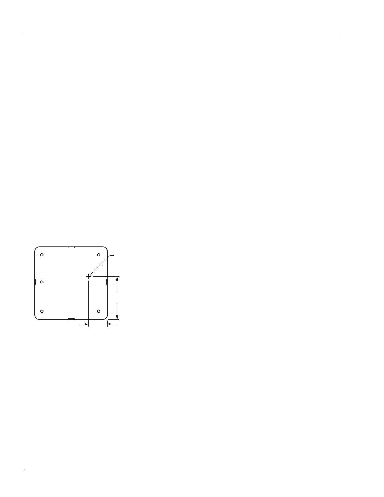
Thermal Considerations
The case temperature must be kept below 100 °C. The
case temperature (T
tion indicated in Figure 8. Therefore, for a particular
current and ambient temperature, the airflow at the filter must be adequate.
Example:
Given: I
Therefore ΔT
O, max = 4 A; TA, max = 95 °C
, max allowable = 5 °C
Determine airflow required (Figure 1): v = 2.0 m/s
(400lfm)
VI(-)
GND
I(+)
V
Note: Top view, pin locations are for reference only. Measurements
are shown in millimeters and (inches).
Figure 8. Case Temperature Measurement
Location
C) should be measured at the posi-
V
O(-)
O(+)
V
6.1
(0.24)
MEASURE CASE
TEMPERATURE HERE
12.7
(0.5)
1-0146
Other Considerations
It is essential for good EMI performance that the input
lines not be contaminated with noise after passing
through the filter. Filtered input traces should therefore
be kept away from noise sources such as power modules and switching logic lines. If input voltage sense
traces must be routed past the power modules from the
quiet side of the filter module, they should be filtered at
the point where they leave the quiet input lines. Input
traces should be kept as far away from output power
traces as possible.
The fundamental switching frequency noise spike can
be somewhat reduced by adding a high-frequency
capacitor of a few microfarads across the input lines of
the filter module.
Adding additional components to the input filter to
improve performance usually has very limited payback,
and may actually increase the noise conducted onto
the input lines. Adding Y caps to the input side of the filter module couples any noise in the ground plane
directly into the input lines, usually degrading performance. Adding additional X and Y caps to the power
module side of the filter module produces lowimpedance loops for high-frequency currents to flow,
possibly degrading performance.
Adding additional common-mode or differential-mode
filtering to the power module output leads decreases
the power module output noise, and also frequently
reduces the input noise by decreasing the noise coupled from output leads to input leads. Common-mode
output filtering is particularly important if the load is tied
to chassis ground. If common-mode filtering is added
to the power module output, ensure that remote-sense
leads sense the output voltage before the commonmode filter. Do not use remote-sense on the load side
of an output common-mode filter.
If input noise performance is unsatisfactory after applying the filter module as described previously, the best
remedy is to modify the layout and grounding scheme.
It is often useful to make a model of the power card,
using copper tape and a vector card, to experiment
with various layout and grounding approaches prior to
committing to a printed-wiring board.
88 Lineage Power
Page 9

Data Sheet
October 2009
Other Considerations (continued)
80
70
60
50
40
30
20
LEVEL (dBµV)
10
0
0.15 0.50 1 2 3 4 5 7 10 30
FREQUENCY (MHz)
Figure 9. HW050FG Conducted Noise with Filter
Compared to Class B Limits
80
70
60
50
40
30
20
LEVEL (dBµV)
10
0
0.15 0.50 1 2 3 4 5 7 10 30
FREQUENCY (MHz)
FLTR75V05 Filter Module
75 Vdc Input Maximum, 5 A Maximum
1-0321
1-0322
Figure 10.JAW075A1 Conducted Noise with Filter
Compared to Class B Limits
90
80
70
60
50
40
30
20
LEVEL (dBµV)
10
0
0.15 0.50 1 2 3 4 5 7 10 30
FREQUENCY (MHz)
1-0323
Figure 11.QHW100F1 Conducted Noise with Filter
Compared to Class B Limits
Lineage Power 9
Page 10
FLTR75V05 Filter Module
75 Vdc Input Maximum, 5 A Maximum
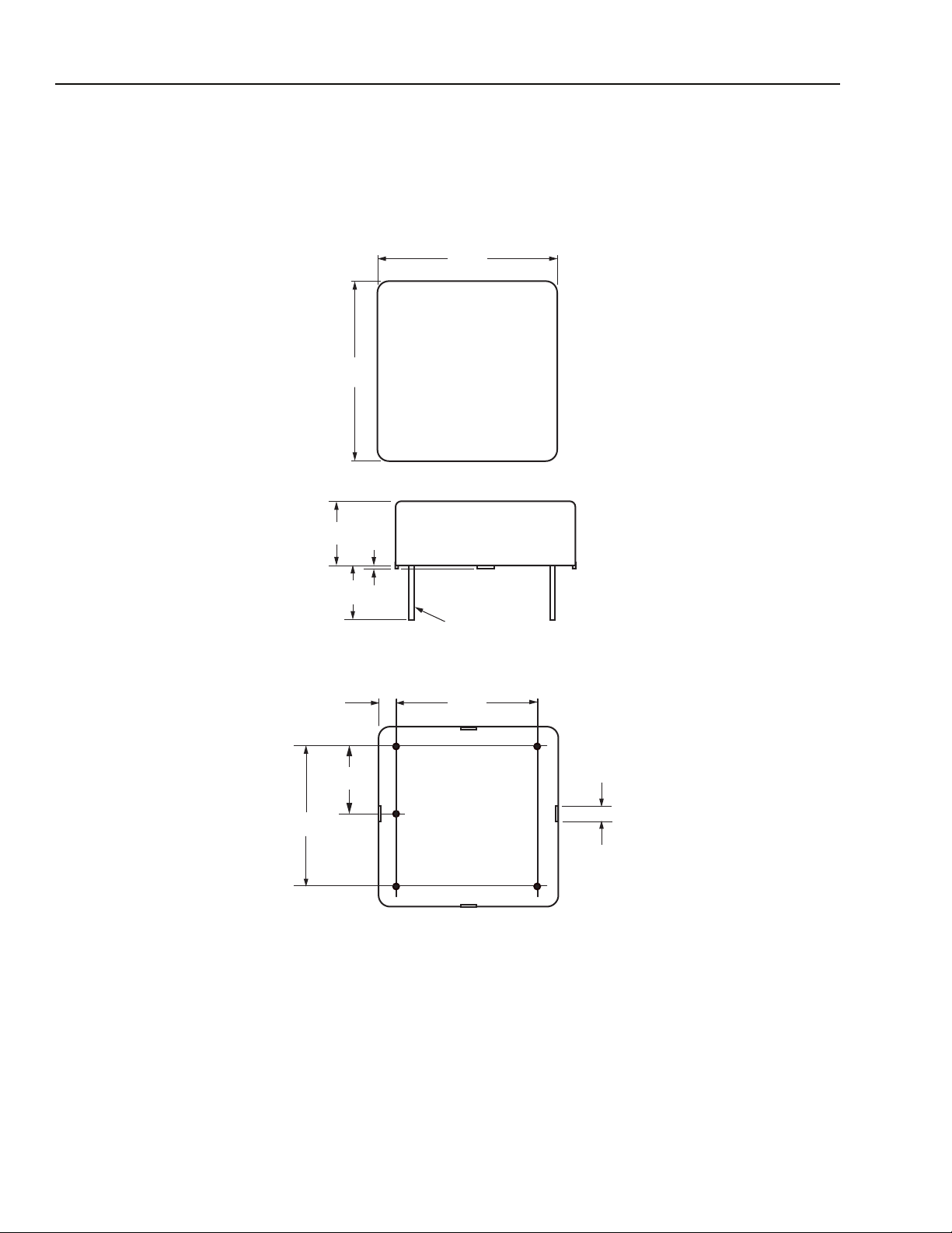
Outline Diagram
Dimensions are in millimeters and (inches).
Tolerances: x.xx ± 0.50 mm (0.02 in.), x.xxx ± 0.250 mm (0.010 in.).
Top View
25.40
(1.000)
25.40
(1.000)
Side View
Data Sheet
October 2009
Bottom View
(0.385)
2.8
(0.11)
19.81
(0.780)
9.78
0.38
(0.015)
8.3 (min)
(0.325 min)
9.91
(0.390)
1.02 (0.040) DIA
SOLDER-PLATED
BRASS, 5 PLACES
19.81
(0.780)
VI(+)
GND
I(-)
V
V
O(+)
V
O(-)
2.03 (0.08
STANDOFFS,
4 PLACES
1-0119
10 Lineage Power
Page 11
Data Sheet
October 2009
Recommended Hole Pattern
Component-side footprint.
Dimensions are in millimeters and (inches).
Tolerances: x.xx ± 0.50 mm (0.02 in.), x.xxx ± 0.250 mm (0.010 in.).
Note: Do not route copper paths beneath power module standoffs.
FLTR75V05 Filter Module
75 Vdc Input Maximum, 5 A Maximum
2.8
(0.11)
19.81
(0.780)
9.91
(0.390)
VI(-)
GND
I(+)
V
19.81
(0.780)
V
O(-)
O(+)
V
STANDOFFS,
4 PLACES
1-0119
Lineage Power 11
Page 12

FLTR75V05 Filter Module
75 Vdc Input Maximum, 5 A Maximum
Post Solder Cleaning and Drying Consideratrions
Post solder cleaning is usually the final circuit-board
assembly process prior to electrical board testing.The
result of inadequate cleaning and drying can affect
both the reliability of a power module and the testability
of the finished circuit-board assembly.For guidance on
appropriate soldering,cleaning and drying procedures,refer to
Modules:Soldering and Cleaning Application Note.
Lineage Power Board Mounted Power
Through-Hole Lead Free Soldering Information
The RoHS-compliant through-Hole products use the
SAC(Sn/Ag/Cu) Pb-free solder and RoHS- compliant
components.They are designed to be processed
through single or dual wave soldering machines.The
pins have an RoHS-compliant finish that is compatible
with both Pb and Pb-free wave soldering processes.A
Maximum preheat rate 3
preheat process should be such that the temperature
of the power module board is kept below 210
solder,the recommended pot temperature is
0
C,while the Pb-free solder pot is 2700C max.Not
260
all RoHS-compliant through-hole products can be processed with paste-through-hole Pb or Pb-free reflow
process.If additional information is needed,please consult with your Lineage Power representative for more details.
0
C/s is suggested.The wave
0
C.For Pb
Data Sheet
October 2009
12 Lineage Power
Page 13

FLTR75V05 Filter Module
75 Vdc Input Maximum, 5 A Maximum
Data Sheet
October 2009
Ordering Information
Please contact your Lineage Power Account Manager or Field Application Engineer for pricing and availability.
Table 1. Device Codes
Device Code Comcode
FLTR75V05 108900739
FLTR75V05Z CC109102654
FLTR75V058Z CC109310818
FLTR75V605Z CC109101433
FLTR75V055Z CC109128237
Optional features may be ordered using the suffixes shown in the Table below.
Option Codes
Option Device Code Suffix
ort pins: 2.79 mm (+0.38 mm/ –0.25 mm)
Sh
(0.110 in. (+0.015 in./ –0.010 in.))
Sh
ort pins: 3.68 mm (+0.38 mm/ –0.25 mm)
(0.145 in. (+0.015 in./ –0.010 in.))
Short pins: 4.57 mm (+0.38 mm/ –0.25 mm)
(0.180 in. (+0.015 in./ –0.010 in.))
Compliant
RoHS
8
6
5
Z
Asia-P acific Head qu arters
Tel: +65 6 41 6 42 83
Eu ro pe, M id dle-East an d Afr ic a He adquar ters
World W i de Headq u arter s
Lineag e Power Corpor ation
Shiloh Roa d, Pla no , TX 75 074, U SA
601
Tyco Electronics Power Systems, Inc.
+1-800-526-781 9
Skyline Drive, Mesquite, TX 75149, USA
3000
(Outs id e U .S.A .: +1- 972-244 -942 8)
-800-526-7819 FAX: +1-888-315-5182
+1
www.l ine agep owe r .co m
utside U.S.A.: +1-972-284-2626, FAX: +1-972-284-2900)
(O
e-m ail: tec h support1 @ lineagep ower .co m
http://power.tycoelectronics.com
Lineage Power reserves the right to ma ke cha nges to the pro duct(s) or in forma tion co ntain ed herein witho ut notice. No liab ility is a ssume d as a res ult of the ir use or
Tyco Electronics Corporation reserves the right to make changes to the product(s) or information contained herein without notice. No liability is assumed as a result of their use or application.
ap
plication. No ri ghts und er any pa tent a ccomp any the sale o f any s uch pr oduct(s) o r info rmation.
No rights under any patent accompany the sale of any such product(s) or information.
Lineage Power DC-DC Products are protected under various patents. Information on these patents is available at www.lineagepower.com/patents
© 2001 Tyco Electronics Corporation Power Systems, Inc., (Mesquite, Texas) All International Rights Reserved.
Printed in U.S.A.
© 2008 Line age Power Co rporation, (P la no , Texas) Al l Inte rnatio nal R ights Res erved.
October 2009
ADS01-0
52EPS (Replaces ADS01-051EPS)
Tel: +49 898 780 672 80
Ind ia Head qu arter s
Tel: +91 8 0 2841 1633
 Loading...