

Page 1
Data Sheet
February 9, 2012
75Vdc Input Voltage Maximum; 12A Output Current Maximum
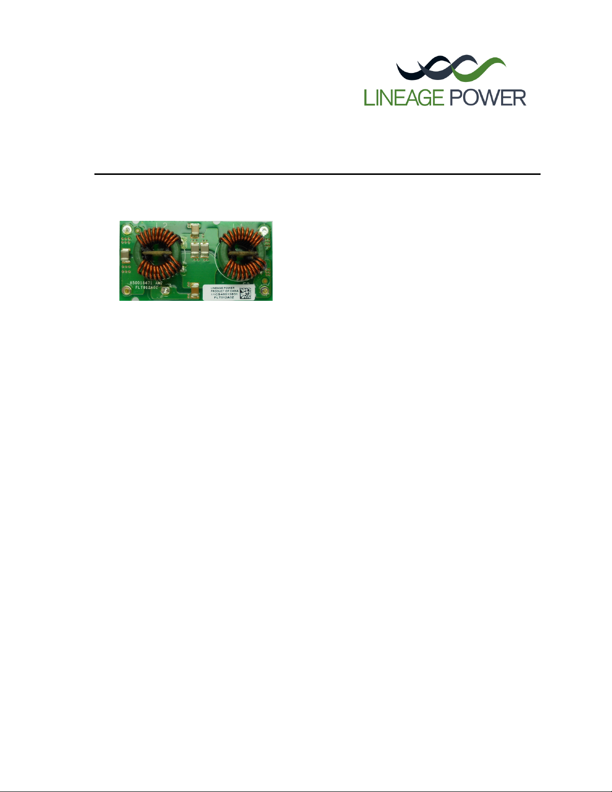
FLT012A0Z/FLT012A0-SZ Input Filter Modules
Applications
Distributed power architectures
Wireless Networks
Enterprise Networks
Access and Optical Network Equipment
Options
Surface Mount Interconnect (-S)
Features
Compliant to RoHS EU Directive 2002/95/EC (Z
versions)
Compatible in a Pb-free or SnPb reflow environment
(Z versions)
Surface Mount and Through hole versions
Common-mode and Differential-mode filtering
Small size and low profile
48.3 mm x 25.4 mm x 11.7 mm
(1.9 in x 1.0 in x 0.46 in)
Same footprint as FLTR100V10 module
Cost efficient open frame design
Wide operating temperature range (-40°C to +85°C)
Meets the voltage isolation requirements for
ETSI 300-132-2
UL* 60950-1, 2
60950-1-07 Certified, and VDE
Licensed
CE mark meets 2006/95/EC directives
ISO** 9001 and ISO 14001 certified manufacturing
facilities
nd
Ed. Recognized, CSA† C22.2 No.
‡
(EN60950-1, 2nd Ed.)
§
Description
The Filter module shall be designed to operate over an input voltage range up to 75Vdc at output current
of 12A in an ambient temperature of -40ºC to 85ºC. The filter module shall be optimized for use with
dc/dc converter modules, to significantly reduce the conducted differential and common-mode noise
returned to the power source. The filter module shall enable designers to meet the requirements of EMI
standards CISPR 22 (EN55022) and FCC Class B by inserting in-line between the power source and the
dc/dc converter module. These modules shall be designed and manufactured to be either surface
mounted
* UL is a re gistered trademark of Underwriters Laboratories, Inc.
†
CSA is a reg istered trademark of Canadian Standards Associat ion.
‡
VDE is a t rademark of Verband Deutscher Elektrotechniker e.V.
** ISO is a registered trademark of the International Orga nization of Standards
§
This product is intended for integration into end-user e quipment . All of the required procedures of end-us e equipment should be followed.
(-S version) or through hole mounted on PCBs.
Document No:DS11-026 ver 1.2
PDF name: FLT012A0Z_FLT012A0-SZ_ds.pdf
Page 2
Preliminary Data Sheet
August 9, 2005
75Vdc Input Voltage Maximum, 7A Output Current Maximum
FLT007A0/FLT007A0-SR Input Filter Modules
Absolute Maximum Ratings
Stresses in excess of the absolute maximum ratings can cause permanent damage to the device. These are
absolute stress ratings only, functional operation of the device is not implied at these or any other conditions in
excess of those given in the operations sections of the data sheet. Exposure to absolute maximum ratings for
extended periods can adversely affect the device reliability.
Parameter Device Symbol Min Max Unit
Input Voltage
Continuous All V
Transient (100ms) V
Operating Ambient Temperature All T
Storage Temperature All T
I/O to Ground Isolation (100% Factory Tested) All
Input to GND Insulation 10 -
IN
0 100 V
IN, TRANS
A
stg
−
0 75 Vdc
-40 85 °C
-55 125 °C
−
1500 Vdc
Ω
M
Electrical Specifications
Unless otherwise indicated, specifications apply over all operating input voltage, resistive load, and temperature
conditions.
Parameter Device Symbol Min Typ Max Unit
Operating Input Voltage All VIN 0 24/48 75 Vdc
Maximum Input-to-Output Current
(VIN= 0 to V
Resistance per leg All R
Maximum Average Current
= 60°C, 2.03 m/s (400lfm) air)
(T
A
Maximum Average Current
= 60°C, natural convection)
(T
A
) All I
iN,max
I
I
max
12 A
max
8 A
max
CAUTION: This power module is not internally fused. An input line fuse must always be used.
This power module can be used in a wide variety of applications, ranging from simple standalone operation to an
integrated part of sophisticated power architecture. To preserve maximum flexibility, internal fusing is not included,
however, to achieve maximum safety and system protection, always use an input line fuse. The safety agencies
require a fast-acting fuse with a maximum rating of 15 A (see Safety Considerations section). Based on the
information provided in this data sheet on inrush energy and maximum dc input current, the same type of fuse with a
lower rating can be used. Refer to the fuse manufacturer’s data sheet for further information.
12 Adc
20
mΩ
2
Page 3
Data Sheet
February 9, 2012
75Vdc Input Voltage Maximum, 12A Output Current Maximum
FLT012A0Z/FLT012A0-SZ Input Filter Modules
Insertion Loss Tables
Parameter Device Symbol Min Typ Max Unit
Common-mode Insertion Loss
50Ω circuit, 500kHz
50Ω circuit, 1MHz
50Ω circuit, 10MHz
Differential-mode Insertion Loss
50Ω circuit, 500kHz
50Ω circuit, 1MHz
50Ω circuit, 10MHz
All
All
All
All
All
All
41 45 dB
51 56
69 75
50 55
52 57
48 53
dB
dB
dB
dB
dB
General Specifications
Parameter Min Typ Max Unit
Calculated MTBF (VIN= V
Telecordia SR 332 Issue 2: Method 1, case 3
Weight
IN, nom
, IO= 0.8I
, TA=40°C)
O, max
⎯
150,609,226 Hours
12 (0.42)
⎯
g (oz.)
LINEAGE POWER 3
Page 4
Data Sheet
February 9, 2012
75Vdc Input Voltage Maximum, 12A Output Current Maximum
FLT012A0Z/FLT012A0-SZ Input Filter Modules
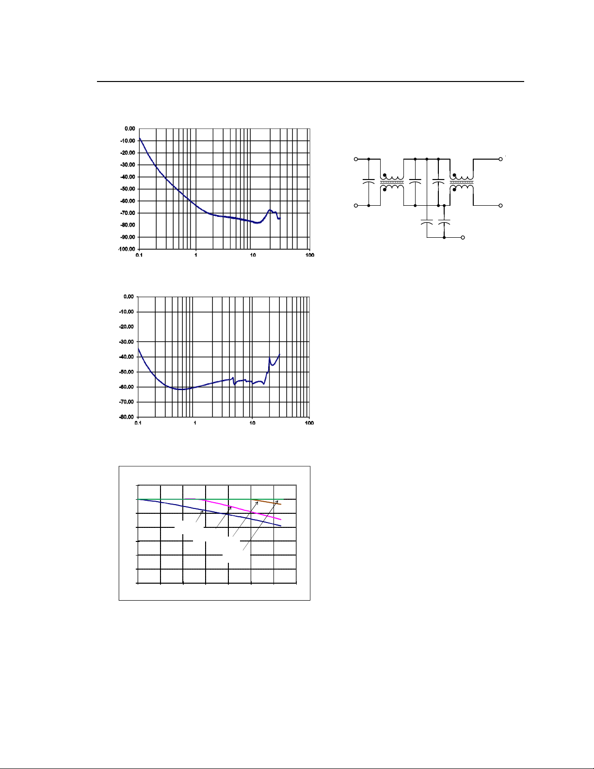
Characteristic Curves
The following figures provide typical characteristics for the FLT012A0 Module.
INSERTION LOSS (dB)
FREQUENCY (MHz)
Figure 1. Typical Common-Mode Insertion Loss in a
50Ω circuit.
INSERTION LOSS (dB)
FREQUENCY (MHz)
Figure 2. Typical Differential-Mode Insertion Loss in a
50Ω circuit.
14
12
10
8
6
4
2
0
20 30 40 50 60 70 80 90
OUTPUT CURRENT, Io (A)
Natural
Convection
00.5m/s
(100lfm)
1m/s
(200lfm)
2m/s
(400lfm)
AMBIENT TEMPERATURE, TA OC
Figure 3. Derating Output Current versus Local
Ambient Temperature and Airflow.
INPUT OUTPUT
15Name = 4488 15Name = 4 488
Figure 4. Internal Schematic
GROUND
LINEAGE POWER 4
Page 5

Data Sheet
E
V
E
February 9, 2012
FLT012A0Z/FLT012A0-SZ Input Filter Modules
75Vdc Input Voltage Maximum, 12A Output Current Maximum
Application Guidelines
Conducted noise on the input power lines can occur
as either differential-mode or common-mode noise
currents. Differential-mode noise is measured
between the two input lines, and is found mostly at
the low frequency end of the spectrum. This noise
shows up as noise at the fundamental switching
frequency and its harmonics. Common-mode noise is
measured between the input lines and ground and is
mostly broadband noise above 10 MHz. The highfrequency nature of common-mode noise is mostly
due to the high-speed switching transitions of power
train components. Either or both types of noise may
be covered in a specification, as well as a
combination of the two.
Differential-mode noise is best attenuated using a
filter composed of line-to-line capacitors (X caps) and
series inductance, provided by either a discrete
inductor or the leakage inductance of a commonmode choke. In addition to the differential filtering
provided by the filter module, it is recommended that
an electrolytic capacitor be located at the converter
side of the filter to provide additional attenuation of
low-frequency differential noise and to provide a low
source impedance for the converter, preventing input
filter oscillations and load transient induced input
voltage dips.
Open-frame DC/DC converter modules and the older
metal-cased DC/DC converter modules require
slightly different filtering arrangements. The
FLT012A0 series of modules are optimized for the
newer open-frame series of modules, but can also be
used with older metal-case modules. The main
differences in filtering recommendations between the
two types of modules are in common-mode filtering,
as explained below.
Filtering Open-Frame DC/DC
Converter Modules
For filtering open-frame DC/DC converter modules,
the recommended circuit is shown in Fig. 5. In
addition to the input electrolytic filter capacitor C1
(recommended value is a minimum of 100uF and
approximately 1uF/W at power levels above 100W),
common-mode filtering capacitors C2 and C3 should
be connected between the input and outputs as
shown. Suitable values for common-mode capacitors
C2 and C3 are in the range between 1000pF to 0.1μF
are usually indicated in the DC/DC converter data
sheet. These capacitors need to be rated for the
isolation voltage desired
sides of the DC/DC converter module. The
recommended power layout of the modules
where the two common-mode capacitors are to be
placed is shown in Fig. 6.
between the input and output
showing
C2
VI(+)
VI(-)
CHASSIS GROUND
FILTER
MODULE
C1
VI(+)
DC/DC
CONVERTER
MODULE
VI(-)
VO(+)
VO(-)
C3
Figure 5. Schematic diagram showing
recommended connection of the FLT012A0 filter
module with open-frame DC/DC converter
modules.
Load
C2
Input
VIN+
VIN-
CHASSIS
GROUND
FLT012A0
MODULE
GND
VO+
VO-
VI+ VO+
C1
CONVERTER
-
V
I
DC/DC
C3
VO+ PLAN
-
V
O
− PLAN
O
Figure 6. Diagram showing recommended layout
of the FLT012A0 filter module with open-frame
DC/DC converter modules.
Filtering Metal-Case DC/DC Converter
Modules
For metal-case DC/DC converter modules with a case
pin, a different filtering arrangement and layout is
recommended. Figure 7 shows the schematic
diagram of the recommended circuit. The main
difference with open-frame module is the use of an
isolated shield plane located underneath the module
which is connected through capacitors C2 through C5
to the input and output connections of the module.
The shield plane along with the case of the module
serves as a Faraday shield helping reduce EMI. The
corresponding layout for metal-case modules is
shown in Fig. 8.
LINEAGE POWER 5
Page 6

Data Sheet
xxx
x
V
February 9, 2012
FLT012A0Z/FLT012A0-SZ Input Filter Modules
75Vdc Input Voltage Maximum, 12A Output Current Maximum
VI(+)
VI(-)
FILTER
MODULE
CHASSIS GROUN D
VI(+)
DC/DC
C1
CONVERTER
MODULE
VI(-)
CASE
C3C2 C4 C5
SHIELD P LANE
VO(+)
VO(-)
Figure 7. Schematic diagram showing
recommended connection of the FLT012A0 filter
module with metal-cased DC/DC converter
modules.
Input
+
V
IN
FLT012A0
GND
VIN-
CHASSIS
GROUND
MODULE
C2
+
V
O
V
−
O
C1
VI+ VO+
DC/DC
CONVERTER
CASE
SHIELD
V
-
I
PLANE
C3
C
C5
4
V
O
Load
-
Figure 8. Diagram showing recommended layout
of the FLT012A0 filter module with metal-case
DC/DC converter modules.
Example Data Showing Results using
the FLT012A0 Modules
Level [dBµV]
80
70
60
x
+
x
+
50
40
30
20
10
0
150k 300k 500k 1M 2M 3M 5M 7M 10M 30M
MES CE1220111019_fin QP
+ MES CE1220111019_fin A
MES CE1220111019_pre PK
MES CE1220111019_pre AV
Frequency [Hz]
+
x
x
x
+
+
+
+
+
Figure 9. Experimental results showing
conducted EMI measured using a FLT012A0
module with a QBVW033 DC/DC converter.
Figure 9 shows example results obtained using a
QBVW033 DC/DC converter module with the
FLT012A0 filter module. The QBVW033 module is
operated at an input voltage of 48V and output
loading corresponding to an input current of 8.7A, a
level close to the 12A capability of the FLT012A0 filter
module. Board capacitance was as per
recommendations in the QBVW033 datasheet. The
results show that the filter module is capable of
meeting EN55022 Class A limits with 11 margin.
LINEAGE POWER 6
Page 7

Data Sheet
W
February 9, 2012
75Vdc Input Voltage Maximum, 12A Output Current Maximum
Thermal Considerations
Power modules operate in a variety of thermal
environments; however, sufficient cooling should
always be provided to help ensure reliable operation.
Considerations include ambient temperature, airflow,
module power dissipation, and the need for increased
reliability. A reduction in the operating temperature of
the module will result in an increase in reliability. The
thermal data presented here is based on physical
measurements taken in a wind tunnel. The test setup is shown in Fig. 10. Note that the airflow is parallel
to the long axis of the module as shown in Fig. 10.
x
12.7_
(0.50)
Air
flow
25.4_
(1.0)
76.2_
(3.0)
used in the
ref
Power Module
Probe Location
for measuring
airflow and
ambient
temperature
o
C.
ind Tunnel
PWBs
Figure 10. Thermal Test Set-up.
The thermal reference point, T
specifications is shown in Figure 11. For reliable
operation this temperature should not exceed 130
The output power of the module should not exceed
the rated output current of the module.
Please refer to the Application Note “Thermal
Characterization Process For Open-Frame BoardMounted Power Modules” for a detailed discussion of
thermal aspects including maximum device
temperatures.
FLT012A0Z/FLT012A0-SZ Input Filter Modules
Figure 11. T
Temperature measurement
ref
location.
Surface Mount Information
Pick and Place
The FLT012A0-SR SMT modules use an open frame
construction and are designed for a fully automated
assembly process. The modules are fitted with a
label designed to provide a large surface area for pick
and place operations. The label meets all the
requirements for surface mount processing, as well as
safety standards, and is able to withstand reflow
temperatures of up to 300
product information such as product code, serial
number and location of manufacture.
Nozzle Recommendations
The module weight has been kept to a minimum by
using open frame construction. Even so, these
modules have a relatively large mass when compared
to conventional SMT components. Variables such as
nozzle size, tip style, vacuum pressure and pick &
placement speed should be considered to optimize
this process. The minimum recommended nozzle
diameter for reliable operation is 5 mm. The maximum
nozzle outer diameter, which will safely fit within the
allowable component spacing, is 8 mm max.
Figure 12. Pick and Place Location.
o
C. The label also carries
LINEAGE POWER 7
Page 8

Data Sheet
February 9, 2012
FLT012A0Z/FLT012A0-SZ Input Filter Modules
75Vdc Input Voltage Maximum, 12A Output Current Maximum
Bottom Side / First Side Assembly
This module is not recommended for assembly on the
bottom side of a customer board. If such an assembly
is attempted, components may fall off the module
during the second reflow process.
Tin Lead Soldering
The FLT012A0-SZ power modules are lead free
modules and can be soldered either in a lead-free
solder process or in a conventional Tin/Lead (Sn/Pb)
process. It is recommended that the customer review
data sheets in order to customize the solder reflow
profile for each application board assembly. The
following instructions must be observed when
soldering these units. Failure to observe these
instructions may result in the failure of or cause
damage to the modules, and can adversely affect
long-term reliability.
In a conventional Tin/Lead (Sn/Pb) solder process
peak reflow temperatures are limited to less than
o
235
C. Typically, the eutectic solder melts at 183oC,
wets the land, and subsequently wicks the device
connection. Sufficient time must be allowed to fuse
the plating on the connection to ensure a reliable
solder joint. There are several types of SMT reflow
technologies currently used in the industry. These
surface mount power modules can be reliably
soldered using natural forced convection, IR (radiant
infrared), or a combination of convection/IR. For
reliable soldering the solder reflow profile should be
established by accurately measuring the modules CP
connector temperatures.
300
250
200
150
10 0
REFLOW TEMP (°C)
50
0
Figure 13. Reflow Profile for Tin/Lead (Sn/Pb)
process.
P eak Temp 23 5oC
Heat zo ne
oCs-1
max 4
So ak zone
30-240s
Preheat zo ne
oCs-1
max 4
REFLOW TIME (S)
Cooling
zo ne
oCs-1
1- 4
T
above
lim
o
C
205
240
235
230
225
220
215
210
MAX TEMP SOLDER (°C)
205
200
0 10 203040 5060
Figure 14. Time Limit Curve Above 205oC Reflow
for Tin Lead (Sn/Pb) process.
Lead Free Soldering
The FLT012A0-SZ SMT modules are lead-free (Pbfree) and RoHS compliant and are both forward and
backward compatible in a Pb-free and a SnPb
soldering process. Failure to observe the instructions
below may result in the failure of or cause damage to
the modules and can adversely affect long-term
reliability.
Pb-free Reflow Profile
Power Systems will comply with J-STD-020 Rev. C
(Moisture/Reflow Sensitivity Classification for
Nonhermetic Solid State Surface Mount Devices) for
both Pb-free solder profiles and MSL classification
procedures. This standard provides a recommended
forced-air-convection reflow profile based on the
volume and thickness of the package (table 4-2). The
suggested Pb-free solder paste is Sn/Ag/Cu (SAC).
The recommended linear reflow profile using
Sn/Ag/Cu solder is shown in Figure. 15. Soldering
outside of the recommended profile requires testing to
verify results and performance.
MSL Rating
The FLT012A0-SRZ SMT modules have a MSL rating
of 2a.
Storage and Handling
The recommended storage environment and handling
procedures for moisture-sensitive surface mount
packages is detailed in J-STD-033 Rev. A (Handling,
Packing, Shipping and Use of Moisture/Reflow
Sensitive Surface Mount Devices). Moisture barrier
bags (MBB) with desiccant are required for MSL
ratings of 2 or greater. These sealed packages
should not be broken until time of use. Once the
original package is broken, the floor life of the product
at conditions of <= 30°C and 60% relative humidity
varies according to the MSL rating (see J-STD-033A).
The shelf life for dry packed SMT packages will be a
LINEAGE POWER 8
Page 9

Data Sheet
February 9, 2012
minimum of 12 months from the bag seal date, when
stored at the following conditions: < 40° C, < 90%
relative humidity.
75Vdc Input Voltage Maximum, 12A Output Current Maximum
FLT012A0Z/FLT012A0-SZ Input Filter Modules
drying procedures, refer to Lineage Power Board
Mounted Power Modules: Soldering and Cleaning
Application Note.(AN04-001)
Per J-STD-020 Rev. C
300
250
200
150
Heat in g Zo ne
1°C/Second
100
Reflow Temp (°C)
50
0
Peak Temp 260°C
Reflow Time (Seconds )
* Min. Time Above 235°C
15 Sec onds
*Time Above 217°C
60 Seconds
Cooling Zone
4°C/Second
Figure 15. Recommended linear reflow profile
using Sn/Ag/Cu solder.
Post solder Cleaning and Drying
Considerations
Post solder cleaning is usually the final circuit-board
assembly process prior to electrical board testing. The
result of inadequate cleaning and drying can affect
both the reliability of a power module and the
testability of the finished circuit-board assembly. For
guidance on appropriate soldering, cleaning and
Through-Hole Lead-Free Soldering
Information
The RoHS-compliant through-hole products use the
SAC (Sn/Ag/Cu) Pb-free solder and RoHS-compliant
components. They are designed to be processed
through single or dual wave soldering machines. The
pins have an RoHS-compliant finish that is compatible
with both Pb and Pb-free wave soldering processes.
A maximum preheat rate of 3°C/s is suggested. The
wave preheat process should be such that the
temperature of the power module board is kept below
210°C. For Pb solder, the recommended pot
temperature is 260°C, while the Pb-free solder pot is
270°C max. Not all RoHS-compliant through-hole
products can be processed with paste-through-hole
Pb or Pb-free reflow process. If additional information
is needed, please consult with your Lineage Power
representative for more details.
LINEAGE POWER 9
Page 10

Data Sheet
February 9, 2012
75Vdc Input Voltage Maximum, 12A Output Current Maximum
FLT012A0Z/FLT012A0-SZ Input Filter Modules
Mechanical Outline
Dimensions are in millimeters and [inches].
Tolerances: x.x mm ± 0.5 mm [x.xx in. ± 0.02 in.] (Unless otherwise indicated)
x.xx mm ± 0.25 mm [x.xxx in ± 0.010 in.]
FLT012AZ (Through Hole Version)
Page 11

Data Sheet
February 9, 2012
75Vdc Input Voltage Maximum, 12A Output Current Maximum
Surface Mount Outline Drawing
FLT012A0Z/FLT012A0-SZ Input Filter Modules
Page 12

Data Sheet
February 9, 2012
75Vdc Input Voltage Maximum, 12A Output Current Maximum
FLT012A0Z/FLT012A0-SZ Input Filter Modules
Recommended Pad Layout
Dimensions are in millimeters and [inches].
Tolerances: x.x mm ± 0.5 mm [x.xx in. ± 0.02 in.] (Unless otherwise indicated)
x.xx mm ± 0.25 mm [x.xxx in ± 0.010 in.]
FLT012A0 (Through Hole Version)
FLT012A0-SR (SMT Version)
Page 13

Data Sheet
a
©
February 9, 2012
75Vdc Input Voltage Maximum, 12A Output Current Maximum
FLT012A0Z/FLT012A0-SZ Input Filter Modules
Ordering Information
Please contact your Lineage Power Sales Representative for pricing, availability and optional features.
Table 1. Device Codes
Device Code
FLT012A0Z 0 – 75Vdc 12A TH CC109172202
FLT012A0-SZ 0 – 75Vdc 12A SMT CC109172210
-Z refers to RoHS-compliant codes
Input
Voltage Range
Output
Current
Connector
Type
Comcodes
Asia-Pacific Headquarters
Tel: +65 6593 7 211
World Wide Headquarters
Lineage Power Corporation
601 Shil oh Roa d, Plano, TX 75074, USA
+1-800 -526-7819
(Outsi de U.S.A.: +1-97 2-244 -9428)
www.lineagepower.com
e-mail: techs uppor t1@li neagep ower.c om
Linea ge Power reser ves th e right to mak e change s to the p roduct(s) o r informat ion conta ined herei n without not ice. No liab ility is ass umed as a result o f their use o r
pplication . No righ ts under any patent accompany the sal e of any s uch produc t(s) or informati on.
Linea ge Power D C-D C pro ducts are p rote cted under variou s patents . Informa tion on the se patents is avail able at www .line agepower .com/paten ts.
2009 Line age Power Corporation, (Plano, Texas) All Inte rn ation al Rights Reserv ed.
Europe, Middle-Ea st and Africa Headquarters
Tel: +49 898 78 0 672 80
India Headquarters
Tel: +91 80 284 11633
PDF name: FLT012A0Z_FLT012A0-SZ_ds.pdf
Document No:DS11-026 ver 1.2
 Loading...