

Page 1

DEH41181
Rev01
g
SMR2 Modbus User Manual
Page 2

Page 3

SMR2 Modbus User Manual
Table of Contents
Introduction .......................................................................................................................2
RTU Transmission Mode .......................................................................................................................... 2
Message frame............................................................................................................................................ 2
RTU Mode Message Frames ...................................................................................................................... 2
Message Format.......................................................................................................................................... 2
Electrical Interface .............................................................................................................2
Communication Environment...........................................................................................3
Register Map .....................................................................................................................2
Fixed Value Registers ................................................................................................................................. 2
Dynamic Value Registers............................................................................................................................ 7
Interpretation of SOS values...................................................................................................................... 9
Setpoint Registers....................................................................................................................................... 9
Event Registers......................................................................................................................................... 13
Interpretation of Event Codes.................................................................................................................. 15
Bit position in Bit map............................................................................................................................. 16
i
Page 4

SMR2 Modbus User Manual
Introduction
The SMR2 trip unit has an optional communications
module that facilitates monitoring of the trip unit via a
master Modbus device. Monitoring features include
breaker settings and the breaker status.
Communication with the SMR2 trip unit requires a
FAMECM module powered externally that provides
isolation and protection.
The Modbus communication protocol is a single
master multi-slave protocol that is hardware
independent and it interfaces with a 2-wire RS485
interface. A single master device initiates and controls
all communication with the other slave devices on the
network. A computer with a serial port and an external
RS-232/RS-485 converter can be used as the mastermonitoring device. The SMR II trip unit is always the
slave and cannot initiate communication. The
maximum number of devices on a Modbus network is
32, i.e. only 31 slave devices can be connected to a
master.
MODBUS devices usually include a Register Map.
MODBUS functions operate on Register map registers
to monitor, configure, and control module I/O. You
should refer to the Register map for your device to gain
a better understanding of its operation.
The transmission mode defines the bit contents of the
message bytes transmitted along the network, and how
the message information is to be packed into the
message stream and decoded.
Standard MODBUS networks employ one of two types
of transmission modes:
i) ASCII Mode ii) RTU Mode
The mode of transmission is usually selected along
with other serial port communication parameters
(baud rate, parity, etc.) as part of the device
configuration.
RTU Transmission Mode
In RTU (Remote Terminal Unit) Mode, each 8-bit
message byte contains two 4-bit Hexadecimal
characters, and the message is transmitted in a
continuous stream. The greater effective character
density increases throughput over ASCII mode at the
same baud rate.
Message frame
A message frame is used to mark the beginning and
ending point of a message allowing the receiving device
to determine which device is being addressed and to
know when the message is completed. It also allows
partial messages to be detected and errors flagged as a
result.
A MODBUS message is placed in a message frame by
the transmitting device. Each word of this message
(including the frame) is also placed in a data frame
that appends a start bit, stop bit, and parity bit.
In ASCII mode, the word size is 7 bits, while in RTU
mode; the word size is 8 bits. Thus, every 8 bits of an
RTU message is effectively 11 bits when accounting for
the start, stop, and parity bits of the data frame.
RTU Mode Message Frames
RTU mode messages start with a silent interval of at
least 3.5 character times. Implemented as a multiple of
character times at the baud rate being used on the
network. The first field transmitted is the device
address. The allowable characters transmitted for all
fields are hexadecimal values 0-9, A-F. A networked
device continuously monitors the network, including
the silent intervals, and when the first field is received
(the address) after a silent interval of at least 3.5
character times, the device decodes it to determine if it
is the addressed device. Following the last character
transmitted, a similar silent interval of 3.5 character
times marks the end of the message and a new message
can begin after this interval.
The entire message must be transmitted as a
continuous stream. If a silent interval of more than 1.5
character times occurs before completion of the frame
(not a continuous stream), the receiving device flushes
the incomplete message and assumes the next byte will
be the address field of a new message.
In similar fashion, if a new message begins earlier than
3.5 character times following a
previous message, the receiving device assumes it is a
continuation of the previous message. This will
generate an error, as the value in the final CRC field
will not be valid for the combined messages.
Message Format
The Modbus RTU Protocol is strictly based upon a
transaction scheme where a master device generates a
query and a slave device replies with a response. Each
query and response message transaction consists of the
following four parts
2
Page 5

SMR2 Modbus User Manual
MODBUS ADDRESSES
The master device addresses a specific slave device by
placing the 8-bit slave address in the address field of the
message (RTU Mode). The address field of the
message frame contains two characters (in ASCII
mode), or 8 binary bits (in RTU Mode). Valid
addresses are from 1-247.
When the slave responds, it places its own address in
this field of its response to let the master know which
slave is responding.
MODBUS FUNCTIONS
The function code field of the message frame will
contain two characters (in ASCII mode), or 8 binary
bits (in RTU Mode) that tell the slave what kind of
action to take. Valid function codes are from 1-255, but
not all codes will apply to a module and some codes are
reserved for future use.
MODBUS DATA FIELD
The data field provides the slave with any additional
information required by the slave to complete the
action specified by the function code. The data is
formed from a multiple of character bytes (a pair of
ASCII characters in ASCII Mode), or a multiple of two
hex digits in RTU mode, in range 00H-FFH. The data
field typically includes register addresses; count values,
and written data. If no error occurs, the data field of a
response from a slave will return the requested data. If
an error occurs, the data field returns an exception
code that the master's application software can use to
determine the next action to take.
The resulting value is compared to the error check
field.
Transmission errors occur when the calculated
checksum is not equal to the Checksum stored in the
incoming packet. The receiving device ignores a bad
packet.
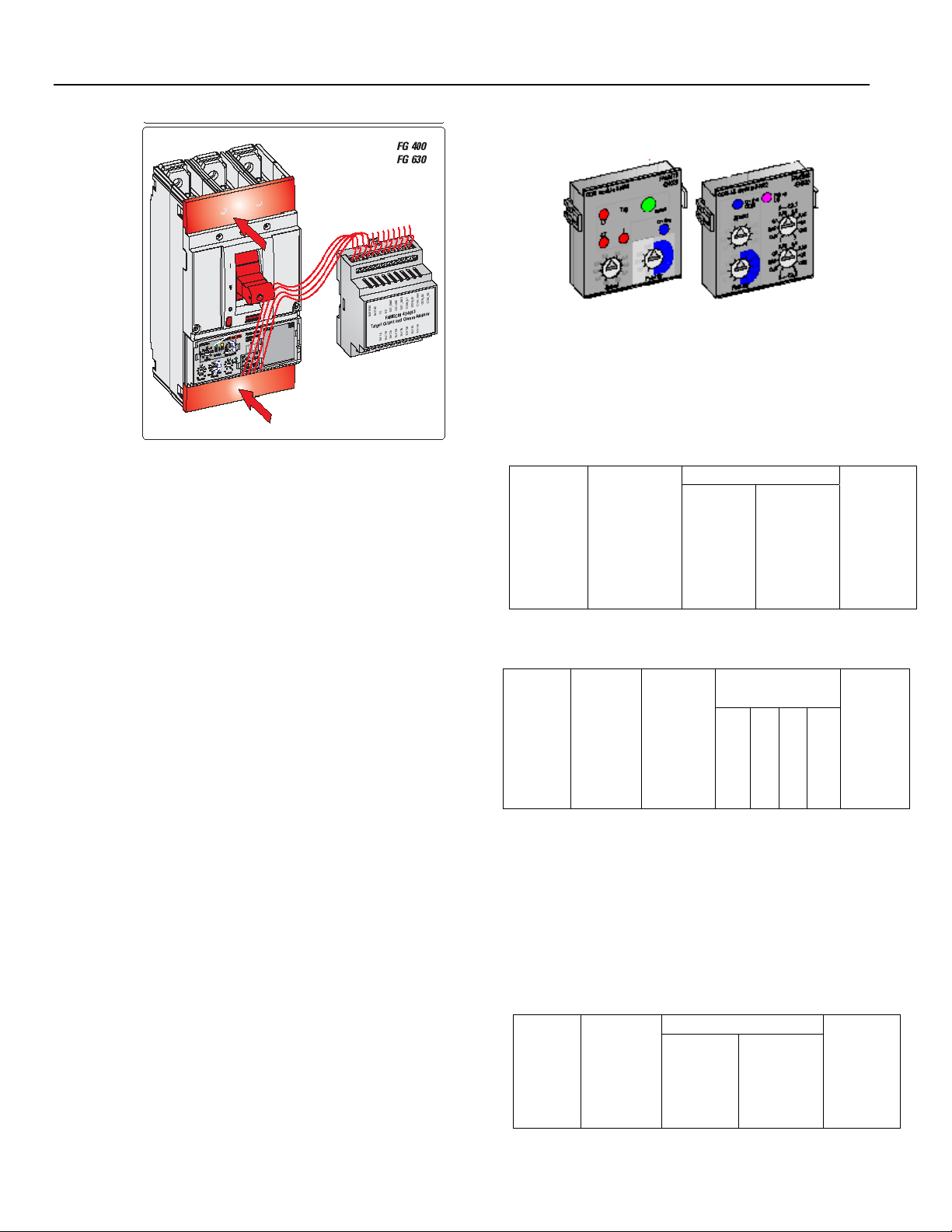
Electrical Interface
The electrical interface is 2-wire RS485 where data flow
is bi-directional and half duplex. RS-485 lines from the
master device should be connected to a FAMECM
module, which is powered externally using a 19-29 VDC
power supply. Refer Figure 1 and 2.
The following wire types are recommended for network
wiring: Belden 3074F – Data Tray 600 V industrial
twinax 18 AWG (7X26); or Belden 9841 – 300 V
communication cable 24 AWG (7X32); or Alpha 6412 –
300 V Communication cable 24 AWG (7x32). Shielded
wire should always be used to minimize noise. Polarity
is important in RS485 communications and each '+'
terminal of every device must be connected together for
the system to communicate.
CRC Error Checking
RTU Mode message frames include an error checking
method that is based on a Cyclical Redundancy Check
(CRC). The error-checking field of a message frame
contains a 16-bit value (two 8-bit bytes) that contains
the result of a Cyclical Redundancy Check (CRC)
calculation performed on the message contents.
The checksum field lets the receiving device determine
if a packet is corrupted with transmission errors. In
Modbus RTU mode, a 16-bit Cyclic Redundancy Check
(CRC-16) is used. The sending device calculates a 16bit value, based on every byte in the packet, using the
CRC-16 algorithm. The calculated value is inserted in
the error check field.
The receiving device performs the calculation, without
the error check field; on the entire packet it receives.
Figure1. Connection between ETU and FAMECM
module
2
Page 6
SMR2 Modbus User Manual
The communication happens at 19200bps with a
Modbus address of 100
Figure2. Connection between Breaker and FAMECM
module
Communication Environment
• The trip unit is always the slave and cannot
initiate communication
• All the registers are read-only
• Hardware layer
RS485: Data moves serially on a 2-wire differential line
(used for TX as well as Rx i.e.; half- duplex)
N-8-1, no parity, 1 start bit, 8 data bits & 1 stop bit (10
bits per character)
• Communication Protocol
RTU Modbus Master-Slave protocol Commandresponse (half-duplex) Min delay between messages is
3.5 char time Max delay within message is 1.5 char
time.
Slave Response time: minimum 3.5 char;
maximum 50mS + 1mS per register
Register order: MSB first, then LSB
• In the presence of a communication
module on Trip unit
A pair of rotary switch decides the Modbus address (0
to 255)
A pair of slide switch decides the baud rate (2400, 4800,
9600 or 19200bps). These switches are available on the
backside of the module
• In the absence of a communication
module on Trip unit
Figure3. Communication modules used with trip unit
Modbus Message Frames
Master’s Query
Data
Start
Data
Byte1
(n bytes)
(n bytes)
No. of
Registers
(2 bytes)
(n bytes)
Byte2
No. of
Registers
(2
bytes)
..
CRC
(2 bytes)
(2bytes)
Byte n
CRC
bytes)
CRC
(2
Slave
Address
(1 byte)
Function
Code
(1 byte)
Address
(2 bytes)
Slave’s Response
Slave
Address
(1byte)
Functio
n Code
(1 byte)
Number
of Bytes
(1 byte)
Examples :
Read Holding Registers (Function Code 03)
Use this command to read setpoint or fixed value
registers. It specifies the starting register and the
number of registers to be read. Read the registers 30103012 from device 100:
Slave
Addres
s
(1
byte)
Function
Code
(1 byte)
Data
Start
Address
(2
bytes)
3
Page 7

SMR2 Modbus User Manual
A
A
64h
Response: (register contents: 3010 = 022Bh, 3010 = 0000h,
3012 = 0066h)
Slave
Addres
s
(1byte)
64h
Read Input Registers (Function Code 04)
Use this command to read dynamic value or event
registers. Read the registers 1058 – 1060 from device
100:
Query:
Slave
Address
(1 byte)
64h
Response: (register content: 1058 = FFFFh, 1059 = A01Ah,
1060 11B1h)
Slave
Addres
s
(1
byte)
64h
Force Single Coil (Function Code 05)
Use this command to perform remote control. This
command sets a single coil to enter ON or OFF.
Force coil 4 of device 100 ON (FF00h force on, 0000h
force off)
Query:
Slave
Address
(1 byte)
Functio
n Code
(1 byte)
03h
Function
Code
(1 byte)
Function
Code
(1 byte)
04h
Function
Code
(1 byte)
03h
04h
0Bh
C2h
Numbe
r of
Bytes
(1byte)
06h
02h 2Bh 00h
Data
Start
Address
(2 bytes)
04h 22h 00h 03h
Number
of Bytes
(1 byte)
06h
FFh FFh A0h
Data
Coil
Address
(2 bytes)
00h
03h
Data
(n bytes)
Byte1
Byte2
00h 00h 66h
(n bytes)
No. Of
Registers
(2 bytes)
Data
(n bytes)
Byte2
-------
Byte1
1Ah 11h B1h
(n bytes)
Data
(2
bytes)
CRCl
CRCh
CRC
-------
(2
bytes
Byte n
)
CRCl
CRC
h
CRC
(2 bytes)
CRCl
CRCh
CRC
(2
bytes)
Byte n
CRCl
CRCh
CRC
(2 bytes)
64h
05h
00h 04h FFh 00h
CRCl
CRCh
Response: (echo query message)
Data
Coil
(n bytes)
Data
(2
bytes)
CRC
CRCl
(2 bytes)
CRCh
Slave
Address
(1 byte)
64h
Function
Code
(1 byte)
05h
Address
(2 bytes)
00h 04h FFh 00h
Preset Single Register (Function Code 06)
Use this command to write to a register. This presets a
value into a single holding register.
Preset register 0002 to 00 03 hex in slave device 17.
Query:
Data
Slave
Address
(1 byte)
11h
Function
Code
(1 byte)
06h
Register
(2 bytes)
00h 02h 00h 03h
(n bytes)
ddress
No. of
Registers
(2 bytes)
CRC
(2 bytes)
CRCl
CRCh
Response (echo query message)
Data
Slave
Address
(1 byte)
Function
Code
(1 byte)
Register
(2 bytes)
(n bytes)
ddress
No. of
Registers
(2
(2 bytes)
CRC
bytes)
11h
06h
00h 02h 00h 03h
CRCl
CRCh
Retransmit Last Message (Function Code 56)
Query:
Slave Address
(1 byte)
64h
Function Code
(1 byte)
38h
CRCl CRCh
CRC
(2 bytes)
Response
Slave Function
Data
(n bytes)
CRC
4
Page 8

Addres
s
(1
byte)
64h
Code
(1 byte)
38h
Previous transmitted
data
xxh xxh xxh xxh xxh
xxh xxh xxh xxh
(2 bytes)
CRCl
CRCh
Exception Response
If the slave receives a message without a
communications error, but is unable to process it, the
slave will return an exception response to inform the
master of the error. The high order bit will be set in
the function code and returned with the characterizing
exception response code:
01h - Invalid Function Code
The Function Code is not recognized or defined by the
SMR2.
02h - Invalid register
The Register address is not recognized or defined by
the SMR2
05h – Acknowledge
The SMR2 has accepted the request and is processing
it, but a long duration of time will be required to do so.
This response is returned to prevent a timeout error
from occurring in the master.
06h - Slave busy
Function
Code
Command Purpose Register Group
SMR2 Modbus User Manual
The SMR2 is busy processing a long duration
command. The master should retransmit the message
latter when the slave is free.
84h - Partial register access error
Command reads or writes to a register that represents
only part of the SMR2 register address. The multiple
register addresses must be read or written together.
Example: Long Time SOS consumes 2 register
addresses, thus both must be read together.
85h - Write protect violation
Command writes to a valid Register, which is defined as
Read Only.
88h - Invalid coil
The Coil address is not recognized or defined by the
SMR2.
Function Codes
The Modbus functions listed in below are supported:
03 Read Holding Registers Reading the setpoint
registers
04 Read Input Registers Reading actual value
registers
05 Force Single Coil Setting the signal coil or
executing single
command
06 Preset Single Register Write Data into single
Register
16
10 hex
56 Retransmit last message Retransmit last message N/A
Preset Multiple Registers Write Data into multiple
Registers
5
Setpoint registers, Fixed value registers
Actual value registers and event registers
Command coils
Setpoint registers, Fixed value registers
Setpoint registers, Fixed value registers
Page 9

SMR2 Modbus User Manual
Register Map
While modbus communication with Target
Communication Accessory module, all the registers are
read only registers. None of them can be written. But
while Modbus communication with Test Kit, most of
the Fixed value & Setpoint registers can be read as well
as written.
Fixed value registers start at 0000 and are read by
Function Code 03.
Actual value registers start at 1000 and are read by
Function Code 04.
Register
address
0000 Product Id 0-65535
0001 ETU Serial Number
0002 ETU Serial Number
0003 ETU Date Code
0004 ETU Date Code low 0-9999
0005
0006
Contents Range Type R/W Format
0-65535
high
0-65535
low
0-9999
high
Frame Size 1 to 3
Amp Rating 1 to 13 Normal
Event registers start at 2000 and are read by Function
Code 04.
Setpoint registers start at 3000 and are read by Function
Code 03.
Writing to the Coil registers, implement supervisory
control through remote commands
All registers composed of 16 bit integers, values less
than 256 stored in lower byte
Fixed Value Registers
Fixed value registers address starts at 0000, read by
Function Code 03. Written with Function code 06/16
(decimal)
The data stored in these registers are the data stored
during trip unit optioning.
Normal
mode –RO
Test mode
--- RW
Normal
mode -- RO
Test mode --
- RW
Normal
mode --- RO
Test mode
--- RW
Normal
mode --- RO
Test mode
--- RW
Normal
mode --- RO
Test mode
--- RW
Normal
mode --- RO
Test mode
--- RW
mode--- RO
Unsigned Int
Unsigned Int
Unsigned Int
Unsigned Int
Unsigned Int
Unsigned Int
1 G400
2 G630
3 K
Unsigned Int
1 7/7
2 25/25
3 60/63
4 125/125
2
Page 10

0007
0008
0009
0010
Information Memory
Option Byte 1
Software revision
number
Product revision
number
Max Number of
events stored
Bitmappe
d 0 to
FFFFh
0000 to
9999
0000 to
9999
Always 8 RO Unsigned Int
Dynamic Value Registers
Actual value registers start at 1000, read by Function
Code 04.All the dynamic value registers are 32-bit in
length. Hence, query of any variable results in two
Modbus register reads, each of 16-bit length. Even
numbered register holds upper-16 bits; Odd numbered
register holds lower –16 bits
SMR2 Modbus User Manual
Test mode
-- RW
Normal
mode--- RO
___________
Test mode
--- RW
RO 4 digit BCD
Normal
mode --- RO
Test mode
--- RW
Example: To find out Phase-A SOS, A Modbus query to
read 1002 and 1003 registers need to be sent to SMR2
by the master.
There are 32 bits in this data. The upper-16 bits would
appear in register 1002 and lower-16 bits in register
1003 as a part of the response.
5 150/160
6 250/250
7 400/400
8 600/630
9 800/800
10 1200/1250
11 1600/1600
12 350
13 500
b0 Instantaneous
0 enabled
1 disabled
b1 Short Time
0 enabled
1 disabled
b2 Long Time
0 enabled
1 disabled
b3 Watchdog
0 enabled
1 disabled
b4 Zone Select Interlock
0 enabled
1 disabled
b5 50-60/400 Hz
Operation
0 50/60 Hz
1 400 Hz
b6 Thermal Watchdog
0 disabled
1-99 enabled
b7 Unused
4 digit BCD
7
Page 11

SMR2 Modbus User Manual
LT Accumulators (A, B, C & N) give normalized values
and are typically max 1.25. Hence, they are multiplied
Reg. Contents Range Type
1000-01 Number of pending
0 - 4294967295 RO Unsigned Int
event
1002-03 SOS Current Phase A 0 - 4294967295 RO Unsigned Int
1004-05 SOS Current Phase B 0 - 4294967295 RO Unsigned Int
1006-07 SOS Current Phase C 0 - 4294967295 RO Unsigned Int
1008-09 SOS Current Phase N 0 - 4294967295 RO
1010-11 LT Accumulator A*1040 - 4294967295 RO Unsigned Int
1012-13 LT Accumulator B*1040 - 4294967295 RO Unsigned Int
1014-15 LT Accumulator C*1040 - 4294967295 RO Unsigned Int
1016-17 LT Accumulator N*1040 - 4294967295 RO Unsigned Int
1018-19 ST Accumulator 0 - 4294967295 RO Unsigned Int
1020-21
GF Accumulator
0 - 4294967295 RO Unsigned Int
1022-23 PL Accumulator 0 - 4294967295 RO Unsigned Int
1024-25 Breaker Status
Note:
If system is in pickup
corresponding bit is set to
1.
Battery status 1 indicates
healthy battery.
ZSI active is set 1 when
ZSI is ACTIVE.
When breaker is open
AUXS1bit is set to 1.
Bitmapped 0 to
FFFFh
1026-27 Push-Button Status 0 - 1 RO Unsigned Int
1028-29 Measured ETU
0 - 100 RO Unsigned Int
Temperature
1030-31 ETU Trip Count 0-655350 RO Unsigned int
1032-33 LT Trip Count 0-65535 RO Unsigned int
1034-35 ST Trip Count 0-65535 RO Unsigned int
1036-37 Instantaneous Trip
0-65535 RO Unsigned int
Count
1038-39 GF Trip Count 0-65535 RO Unsigned int
1040-41 PL Trip Count 0-65535 RO Unsigned int
1042-43 Software Fault Trip
0-65535 RO Unsigned int
Count
1044-45 Remote Trip Count 0-65535 RO Unsigned int
1046-47 RP Missing Trip Count 0-65535 RO Unsigned int
1048-49 Flash Erased Count 0-65535 RO Unsigned int
1050-51 No module Trip Count 0-65535 RO Unsigned int
1052-53 Over temperature Trip
0-65535 RO Unsigned int
Count
with 10,000 and sent out on Modbus for reading
purposes.
Format
R/W
Unsigned Int
RO B0: Unused
B1: ST Pickup
B2: GF Pickup
B3: PL Pickup
B4 (unused)
B5: LT 105 Pickup (PU >= 105)
B6: LT 95 Pickup (95 <= PU < 105)
B7: LT 75 Pickup (75 <= PU < 95)
B8: LT 60 Pickup (60 <= PU < 75)
B9: LM 1
B10: LM 2
B11: ZSI active
B12: Battery Status
B13: AUXS1
B14, B15 Unused
1 = Push button is pressed
0 = Push Button is released
8
Page 12

SMR2 Modbus User Manual
Interpretation of SOS values
The Sum Of Squares values (SOS) of a phase is a
measure of the RMS value of current flowing through
that Phase.SMR2 calculates this values in every half
cycle and use this value as a measure of current to
perform the protection algorithm. The no. of current
samples used for SOS calculation depends on the
frequency.
When a current equal to sensor rating (I
) value is
CT
For 500A, 50Hz input current SOS value will be
equal to 1297350.
Example: SOS to current conversion
flowing through the breaker, a SOS value of 830304 will
be displayed if supply frequency is 50 Hz. For 60 Hz,
This value will be 691920.
ICT _SOS_Value for 50 Hz =
ICT _SOS_Value for 60 Hz =
830304
691920
Using this value we can calculate SOS value for any
current or current for any given SOS value.
For given current , SOS value can be calculated
using the following equation:
SOS value
= (input current/sensor rating)
2
x
ICT _SOS_Value
For given SOS value ,Current amplitude can be
calculated using the following equation:
Input current
= (SOS Value /
ICT _SOS_Value
0.5
)
x Sensor Rating
Example: Current to SOS conversion
sensor rating = 400A
Input current=500A
Frequency =50Hz
select
ICT _SOS_Value
based on frequency
If SOS Value= 7472736 for 50 Hz , then
corresponding current is 1200A
Note:
UL/IEC bit (Bit 0) in Control Byte (Modbus Address
3012) is monitored and ETUs operating frequency is
determined based on this bit.
Setpoint Registers
Setpoint registers start at 3000, read by Function Code 03
Reg. Contents Range Type R/W Format
3000 Hour 0 - 23
3001 Minute 0 - 59
Normal
mode - RO
Test mode
RW
Normal
mode - RO
Test mode
RW
SOS value = (input current/sensor
2
x
rating)
ICT _SOS_Value
= (500/400)2 x 830304
= 1297350
Sensor rating = 400A
SOS Value= 7472736
Frequency =50Hz
Select
ICT _SOS_Value based on frequency
Input current = (SOS Value /
_SOS_Value
0.5
)
= (7472736/830304)
= 1200 A
UL/IEC bit (Bit
0) in Control
byte
0 - UL 60 Hz
1 - IEC 50 Hz
Unsigned int
(Unused)
Unsigned int
(Unused)
x Sensor Rating
Line
Frequency
ICT
0.5
x 400
9
Page 13

SMR2 Modbus User Manual
3002 Seconds 0 - 59
3003 Long Time Pickup 0-15 Normal
3004 Long Time delay 0-6 Normal
3005
3006 Short Time delay 0-9 Normal
3007 Ground Fault pickup 0-8 (in GF
Short time pickup 0-9 Normal
module
0-9 (in GFA
module)
Normal
mode - RO
Test mode
RW
Mode--RO
_________
Test Mode
RW
Mode--RO
_________
Test Mode
RW
Mode--RO
---------------------Test Mode
RW
Mode--RO
_________
Test Mode
RW
Normal
Mode--RO
_________
Test Mode
RW
Unsigned int
(Unused)
Unsigned int
0 0.625
1 0.65
2 0.675
3 0.7
4 0.725
5 0.75
6 0.775
7 0.8
8 0.825
9 0.85
10 0.875
11 0.9
12 0.925
13 0.95
14 0.975
15 1.0
Unsigned int
0 Line 1.25
1. Line 2.5
2. Line 5
3. Line 10
4. Motor 20
5. Motor 30
6.
Unsigned int
Value second I2T
0 40ms No
1 120ms No
2 210ms No
3 310ms No
4 420ms No
5 420ms Yes
6 310ms Yes
7 210ms Yes
8 120ms Yes
9 40ms Yes
Unsigned int
0 0.2X
1 0.3X
2 0.4X
3 0.5X
4 0.6X
5 0.7X
6 0.8X
7 0.9X
8 1.0X
10
Page 14

3008 Ground Fault delay 0-9 Normal
Mode
RO
_________
Test Mode
RW
3009 Inst. Pickup 0-9 Normal
Mode--RO
_________
Test Mode
RW
3010 Module Address 0 - 240
3011 Last Trip Data Bitmap
0 - 255
3012 Control Byte Bitmap
0-255
3013 Protection Multiplier 64-100 Normal
3014 Neutral Protection 0-100 Normal
3015 Temperature Limit 0-100 degree C Normal
3016 Product Reject Code Key 0 - 65535 RO
3017 Rating Plug Serial Number
high
3018 Rating Plug Serial Number
low
0-9999 RO
0-9999 Normal
Normal
Mode - RO
Test mode
RW
Normal
Mode--RO
_________
Test Mode
RW
Normal
Mode--RO
_________
Test Mode
RW
Mode --RO
_________
Test Mode
RW
Mode
RO
_________
Test Mode
RW
Mode
RO
_________
Test Mode
RW
mode - RO
SMR2 Modbus User Manual
9 GFA Reset (In GFA module
only)
Value second I2T
0 40ms No
1 120ms No
2 210ms No
3 310ms No
4 420ms No
5 420ms Yes
6 310ms Yes
7 210ms Yes
8 120ms Yes
9 40ms Yes
Unsigned int
Refer to the table
64% 100%
0%, 50%, 100%
11
Page 15

SMR2 Modbus User Manual
Test mode
RW
3019 Rating Plug Date Code
high
3020 Rating Plug Date Code low 0-9999
3021 Rating Plug LT Settings 0 - 255
3022 Number of Data bits 0-1
3023 Number of Stop bits 0-1
3024 Parity 0-2
3025 Baud Rate 0- 3
3026 Modbus Address 1-247 Normal
3027 LM1 Pickup 0-9
3028 LM2 Pickup 0-9
0-9999
Normal
mode – RO
Test mode
RW
Normal
mode - RO
Test mode
RW
Normal
mode - RO
Test mode
RW
Normal
mode RO
Test mode
RW
Normal
mode – RO
Test mode
RW
Normal
mode - RO
Test mode
RW
Normal
mode - RO
Test mode
RW
mode - RO
Normal mode
- RO
Normal mode
- RO
0 7-bits
1 8-bits
0 1-stop bit
1 2-stop bits
0 No parity
1 Even Parity
2 Odd Parity
0 2400
1 4800
2 9600
3 19200
ETU is known by this slave
address in the communication
network and communicates over
this address.
0 0.55
1 0.6
2 0.65
3 0.7
4 0.75
5 0.8
6 0.85
7 0.9
8 0.95
9 1.0
0 0.55
1. 0.6
2. 0.65
3. 0.7
4. 0.75
5. 0.8
6. 0.85
7. 0.9
8. 0.95
9. 1.0
12
Page 16

3029 Flag Cleared Byte 00 &
0xFF
3030 Test Kit Modbus Address 0 - 255 Normal
3031 Test Kit Baud Rate 0 - 3 Normal
3032 Ammeter Display Current 0 - 9999 Test mode
3033 Ammeter Display Current
Pushbutton
0 - 9999
Event Registers
The trip unit stores up to eight events, with each event
utilizing 8 registers to describe the details of the event.
Last eight events are stored in chronological order, with
EVENT 1 being the oldest event and EVENT n being
Normal
mode - RO
mode - RO
mode – RO
RW
Normal
mode - RO
Test mode
RW
Normal
mode - RO
the newest. An event is automatically cleared once read
by the host.
SMR2 Modbus User Manual
00 Cleared (trip history can
not be shown on Flag
Module LEDs)
0xFFFF
Not Cleared (trip history can
be shown on Flag Module
LEDs)
This is to test COMM
switches.
This returns the cumulative
Modbus address set through
two COMM switches.
00 – 2400
01 – 4800
02 – 9600
03 – 19200
This is to test DIP switches.
This holds the value which is
displayed on LCD display
Value greater than 9999 will
be displayed as “----“
Alternate value, which can be
written while testing
Ammeter module. As long as
Select_Phase is pushed, this
value gets displayed.
Value greater than 9999 will
be displayed as “----“
13
Page 17

SMR2 Modbus User Manual
If another event occurs before the master reads all the
existing events, the oldest event is lost, new event data
will be placed in the EVENT 8 register, and the older
event register contents are shifted. The total number of
events since the last reset will be kept counted at
register location 1000-1001. Events are read using
Function Code 04.
Reg Contents Units/
2000 Event Code – Event 1 0-256 RO Unsigned int
2001 Hour 0 RO Unsigned int
2002 Minute 0 RO Unsigned int
2003 Second 0 RO Unsigned int
2004 Milliseconds 0 RO Unsigned int
2005 Event specific data 1 0 - 65535 RO Unsigned int
2006 Event specific data 2 0 - 65535 RO Unsigned int
2007 Event specific data 3 0 - 65535 RO Unsigned int
2008 Event code – Event 2 0-256 RO Unsigned int
2009 Hour 0 RO Unsigned int
2010 Minute 0 RO Unsigned int
2011 Second 0 RO Unsigned int
2012 Milliseconds 0 RO Unsigned int
2013 Event specific data 1 0 - 65535 RO Unsigned int
2014 Event specific data 2 0 - 65535 RO Unsigned int
2015 Event specific data 3 0 - 65535 RO Unsigned int
… … … … …
2056 Event code – Event 8 0-256 RO Unsigned int
2057 Hour 0 RO Unsigned int
2058 Minute 0 RO Unsigned int
2059 Second 0 RO Unsigned int
2060 Milliseconds 0 RO Unsigned int
2061 Event specific data 1 0 - 65535 RO Unsigned int
2062 Event specific data 2 0 - 65535 RO Unsigned int
2063 Event specific data 3 0 - 65535 RO Unsigned int
Range
Type
R/W
Format
14
Page 18

SMR2 Modbus User Manual
Interpretation of Event Codes
The following table describes the meaning of each
event code
Event
Code
(Hex
)
1
2 Short Time O/C trip Fault SOS
3 Instantaneous O/C
4 Ground Fault Trip Fault SOS
5 Phase Loss Trip Phase Loss
6 Remote Trip Bitmap 16-bit
7
8
9
A
B
C
D
E Low Trip Voltage
F Software Fault
10 RAM Failure Bitmap 16-bit
11 ROM Failure Bitmap 16-bit
12
13 Rating Plug Missing Bitmap 16-bit
14 Short Time Switch
15
16 Instant Switch change Bitmap 16-bit
17 Module Switch/Type
18 Short Time Delay
19
1A Module Missing Trip
Meaning Register 1 Register 2 Register 3
Long Time Overcurrent Trip
Trip
Over-Temp Trip
Aux Switch Opened
Warning
Change
Long Time Switch
Change
Change
Switch Change
Long Time Delay
Switch Change
Fault SOS
Current
Current
Instantaneous
Fault Current
Current
Accumulator
Temperature
Bitmap 16-bit
Bitmap 16-bit
Bitmap 16-bit
Bitmap 16-bit
Bitmap 16-bit
Bitmap 16-bit
Bitmap 16-bit
Fault SOS Current
Fault SOS Current
Instantaneous Fault
Current
Fault SOS Current
Phase Loss
Accumulator
15
Page 19

SMR2 Modbus User Manual
Bit position in Bit map
Bit Position in Bitmap Meaning Event code (Hex)
0
1 0 Aux Switch Open
2 0 No Low Trip Voltage Warning
3 0 No RAM Failure
4 0 No ROM Failure
5 0 No Rating Plug Missing
6 0 No Short Time Switch Change
7 0 No Long Time Switch Change
8 0 No Instant Switch change
9 0 No Module Switch/Type Change
10 0 No Short Time Delay Switch Change
11 0 No Long Time Delay Switch Change
12 0 No Missing Module
0 No Remote Trip
1 Remote Trip
1 Aux Switch Closed
1 Low Trip Voltage Warning
1 RAM Failure
1 ROM Failure
1 Rating Plug Missing
1 Short Time Switch Change
1 Long Time Switch Change
1 Instant Switch change
1 Module Switch/Type Change
1 Short Time Delay Switch Change
1 Long Time Delay Switch Change
1 Missing Module
6
C
0E
10
11
13
14
15
16
17
18
19
12
16
Page 20

Page 21

SMR2 Modbus User Manual
g
General Electric Company
41 Woodford Ave., Plainville, CT 06062
DEH41181 Rev01 © 2006 General Electric Company
GE Consumer & Industrial
17
 Loading...