

Page 1
GE
Data Sheet
EVK011A0B Series (Eighth-Brick) DC-DC Converter Power Modules
36–60Vdc Input; 12.0Vdc Output; 11A Output Current
RoHS Compliant
Applications
Distributed Power Architectures
Wireless Networks
Access and Optical Network Equipment
Enterprise Networks including Power over Ethernet
(PoE)
Options
Negative Remote On/Off logic
Over current/Over temperature/Over voltage
protections (Auto-restart)
Features
Compliant to RoHS II EU “Directive 2011/65/EU”
Compliant to REACH Directive (EC) No 1907/2006
Compatible in a Pb-free or SnPb reflow environment
High efficiency – 95% at 12V full load
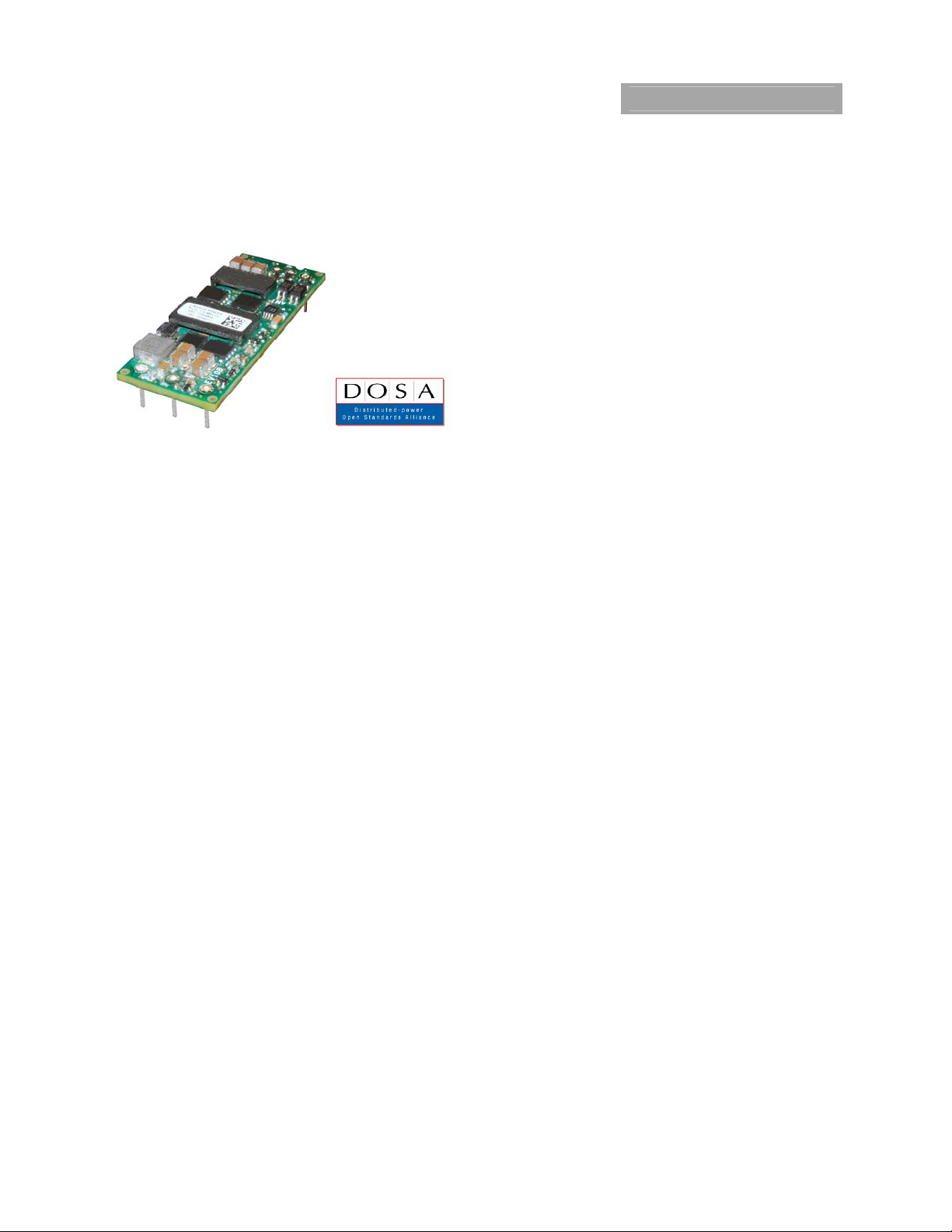
Industry standard, DOSA compliant, Eighth brick footprint
57.9mm x 22.9mm x 8.95mm
(2.28in x 0.90in x 0.352in)
Wide Input voltage range: 36-60 Vdc
Tightly regulated output
Constant switching frequency
Positive Remote On/Off logic
Input under/over voltage protection
Output overcurrent/voltage protection
Over-temperature protection
Remote sense
No minimum load required
No reverse current during output shutdown
Output Voltage adjust: 80% to 110% of V
Operating temperature range (-40°C to 85°C)
UL* 60950-1Recognized, CSA
and VDE
‡
0805:2001-12 (EN60950-1) Licensed
CE mark meets 73/23/EEC and 96/68/EEC directives
Meets the voltage and current requirements for ETSI 300-132-
2 and complies with and licensed for Basic insulation rating
per EN60950-1
2250 Vdc Isolation tested in compliance with IEEE 802.3
standards
**
ISO
9001 and ISO 14001 certified manufacturing facilities
o,nom
†
C22.2 No. 60950-1-03 Certified,
§
¤
PoE
* UL is a registered trademark of Underwriters Laboratories, Inc.
†
CSA is a registered trademark of Canadian Standards Association.
‡
VDE is a trademark of Verband Deutscher Elektrotechniker e.V.
§
This product is intended for integration into end-user equipment . All of the required procedures of end-use equipment should be followed.
¤ IEEE and 802 are registered trademarks of the Institute of Electrical and Electronics Engineers, Incorporated.
** ISO is a registered trademark of th e International Organization of Standards
May 15, 2013 ©2012 General Electric Company. All rights reserved. Page 1
Page 2

GE
Data Sheet
EVK011A0B Series (Eighth-Brick) DC-DC Converter Power Modules
36–60Vdc Input; 12.0Vdc Output; 11A Output Current
Absolute Maximum Ratings
Stresses in excess of the absolute maximum ratings can cause permanent damage to the device. These are absolute stress ratings
only, functional operation of the device is not implied at these or any other conditions in excess of those given in the operations
sections of the data sheet. Exposure to absolute maximum ratings for extended periods can adversely affect the device reliability.
Parameter Device Symbol Min Max Unit
Input Voltage
Continuous All V
Transient (≤10 ms) All V
Operating Ambient Temperature All T
(see Thermal Considerations section)
Storage Temperature All T
I/O Isolation voltage (100% factory Hi-Pot tested) All
IN
IN,trans
A
stg
Electrical Specifications
Unless otherwise indicated, specifications apply over all operating input voltage, resistive load, and temperature conditions.
Parameter Device Symbol Min Typ Max Unit
Operating Input Voltage All VIN 36 48 60 Vdc
Maximum Input Current
(VIN= V
Input No Load Current
(VIN = V
Input Stand-by Current
(VIN = V
to V
IN, min
IN, nom
IN, nom
, IO=I
IN, max
, IO = 0, module enabled)
, module disabled)
O, max
)
All I
All I
All I
IN,max
IN,No load
IN,stand-by
-0.3 60 Vdc
-0.3 75 Vdc
-40 85 °C
-55 125 °C
2250 Vdc
4.0 4.4 Adc
75 mA
20 mA
Inrush Transient All I2t 0.5 A2s
Input Reflected Ripple Current, peak-to-peak
(5Hz to 20MHz, 1μH source impedance; V
IO= I
; See Test configuration section)
Omax
max,
Input Ripple Rejection (120Hz) All 50 dB
IN, min
to V
IN,
All 20 mA
p-p
CAUTION: This power module is not internally fused. An input line fuse must always be used.
This power module can be used in a wide variety of applications, ranging from simple standalone operation to an integrated part
of sophisticated power architectures. To preserve maximum flexibility, internal fusing is not included, however, to achieve
maximum safety and system protection, always use an input line fuse. The safety agencies require a time-delay fuse with a
maximum rating of 8 A (see Safety Considerations section). Based on the information provided in this data sheet on inrush energy
and maximum dc input current, the same type of fuse with a lower rating can be used. Refer to the fuse manufacturer’s data sheet
for further information.
May 15, 2013 ©2012 General Electric Company. All rights reserved. Page 2
Page 3
GE
Data Sheet
EVK011A0B Series (Eighth-Brick) DC-DC Converter Power Modules
36–60Vdc Input; 12.0Vdc Output; 11A Output Current
Electrical Specifications (continued)
Parameter Device Symbol Min Typ Max Unit
Nominal Output Voltage Set-point
VIN=V
IN, min
, IO=I
O, max
, TA=25°C)
All V
O, set
Output Voltage
(Over all operating input voltage, resistive load, and
All V
O
temperature conditions until end of life)
Output Regulation
Line (VIN=V
Load (IO=I
Temperature (T
IN, min
O, min
to V
to I
ref=TA, min
) All
O, max
IN, max
)
to T
) All
A, max
All
Output Ripple and Noise on nominal output
(VIN=V
IN, nom
,IO= I
O, max
, TA=T
A, min
to T
)
A, max
RMS (5Hz to 20MHz bandwidth) All
Peak-to-Peak (5Hz to 20MHz bandwidth) All
External Capacitance All C
Output Current All I
Output Current Limit Inception (Hiccup Mode ) All
(VO= 90% of V
Output Short-Circuit Current
(VO≤250mV) ( Hiccup Mode )
)
O, set
All I
I
O, lim
O, s/c
O
o
Efficiency All η 95 %
VIN= V
IO=I
Switching Frequency (Input ripple is ½ fsw) All f
, TA=25°C
IN, nom
= V
O, max , VO
O,set
sw
Dynamic Load Response
(dIo/dt=0.1A/s; VIN = V
IN, nom
; TA=25°C)
Load Change from Io= 50% to 75% or 25% to 50%
of Io,max;
Peak Deviation All V
Settling Time (Vo<10% peak deviation)
(dIo/dt=1A/s; VIN = V
IN, nom
; TA=25°C)
Load Change from Io= 50% to 75% or 25% to 50%
of Io,max;
Peak Deviation All V
Settling Time (Vo<10% peak deviation)
pk
All t
s
pk
All t
s
11.76 12.0 12.24 V
-3.0
100
0
+3.0 % V
0.2 % V
0.2 % V
1.0 % V
30 mV
100 mV
2,000 μF
11 Adc
105 115 130
3 5 A
% I
dc
O, set
O, set
O, set
O, set
rms
pk-pk
rms
o
330 kHz
3
200
% V
s
O, set
5
200
% V
s
O, set
Isolation Specifications
Parameter Device Symbol Min Typ Max Unit
Isolation Capacitance All C
Isolation Resistance All R
I/O Isolation Voltage (100% factory Hi-pot tested) All All
iso
iso
10
1000
2250 Vdc
pF
MΩ
General Specifications
Parameter Device Symbol Min Typ Max Unit
Calculated Reliability based upon Telcordia SR-332
Issue 2: Method
I Case 3 (I
=80%I
O
O, max
, TA=40°C,
airflow = 200 lfm, 90% confidence)
Weight (Open Frame) All
All FIT 315.1 10
All MTBF 3,173,243 Hours
19
(0.67)
May 15, 2013 ©2012 General Electric Company. All rights reserved. Page 3
9
/Hours
g
(oz.)
Page 4

GE
Data Sheet
EVK011A0B Series (Eighth-Brick) DC-DC Converter Power Modules
36–60Vdc Input; 12.0Vdc Output; 11A Output Current
Feature Specifications
Unless otherwise indicated, specifications apply over all operating input voltage, resistive load, and temperature conditions. See
Feature Descriptions for additional information.
Parameter Device Symbol Min Typ Max Unit
Remote On/Off Signal Interface
(VIN=V
Signal referenced to V
Negative Logic: device code suffix “1”
Logic Low = module On, Logic High = module Off
Positive Logic: No device code suffix required
Logic Low = module Off, Logic High = module On
Turn-On Delay1 and Rise Times
(IO=I
Case 1: On/Off input is set to Logic Low (Module
ON) and then input power is applied (T
instant at which V
Case 2: Input power is applied for at least 1 second
and then the On/Off input is set from OFF to ON (T
instant V
Output voltage Rise time (time for Vo to rise from 10%
of V
Output voltage overshoot – Startup
IO= I
Remote Sense Range All V
(Max voltage drop is 0.5V)
Output Voltage Adjustment Range
Output Overvoltage Protection
Input Undervoltage Lockout All V
Input Overvoltage Lockout All V
Notes:
1. The module has an adaptable extended Turn-On Delay interval, T
rapid cycling of Vin from normal levels to less than the Input Undervoltage Lockout (which causes module shutdown), and then back to normal; or 2) toggling the
on/off signal from on to off and back to on without removing the input voltage. The normal Turn-On Delay interval, T
input voltage removed from the module for the preceding 1 second.
2. Maximum trim up possible only for Vin>40V.
to V
IN, min
Logic Low - Remote On/Off Current All I
Logic Low - On/Off Voltage All V
Logic High Voltage – (Typ = Open Collector) All V
Logic High maximum allowable leakage current All I
O, max , VIN=VIN, nom, TA
on/off
to 90% of V
o,set
; VIN=V
O, max
Turn-on Threshold
Turn-off Threshold
Hysterisis 1.5 2.0
Turn-off Threshold
Turn-on Threshold
Hysterisis 1 2
; open collector or equivalent,
IN, max
terminal)
IN-
on/off
on/off
on/off
on/off
-0.7
2.0 5.0 Vdc
1.0 mA
1.0 Vdc
10 μA
= 25 oC)
= V
until VO = 10% of V
IN
IN, min
toggles until VO = 10% of V
)
o, set
to V
IN, min
, TA = 25 oC
IN, max
2
delay
O, set
from
).
O,set
)
delay
All T
from
All T
All T
All
All 80 110 % V
All V
, of 4 seconds. The extended T
delay
— 25 30 msec
delay
— 12 20 msec
delay
rise
SENSE
O, limit
UVLO
OVLO
— 10 15 msec
— 3 % V
10 % V
13.8
16.5 Vdc
30 34.5 36 Vdc
30 32.5
60 62
64 66 V
will occur when the module restarts following either: 1) the
delay
, will occur whenever a module restarts with
delay
O, set
O, set
O, set
Vdc
Vdc
dc
Vdc
Vdc
May 15, 2013 ©2012 General Electric Company. All rights reserved. Page 4
Page 5

GE
Data Sheet
EVK011A0B Series (Eighth-Brick) DC-DC Converter Power Modules
36–60Vdc Input; 12.0Vdc Output; 11A Output Current
Characteristic Curves
The following figures provide typical characteristics for the EVK011A0B (12V, 11A) at 25oC. The figures are identical for either
positive or negative remote On/Off logic.
(V) (200mV/div)
O
EFFICIENCY, (%)
OUTPUT CURRENT, IO (A) TIME, t (200µs/div)
Io(A) (5A/div) V
OUTPUT CURRENT OUTPUT VOLTAGE
Figure 1. Converter Efficiency versus Output Current. Figure 4. Transient Response to 1.0A/µS Dynamic Load
= V
IN
IN,NOM
(V) (50mV/div)
O
V
OUTPUT VOLTAGE
TIME, t (2s/div)
Figure 2. Typical output ripple and noise (V
o,max).
I
(V) (200mV/div)
O
IN = VIN,NOM, Io
Change from 50% to 75% to 50% of full load (V
=100µF.
C
O
(V) (2V/div)
O
(V) (5V/div) V
On/Off
V
OUTPUT VOLTAGE On/Off VOLTAGE
TIME, t (10ms/div)
Figure 5. Typical Start-up Using Remote On/Off, negative
=
logic version shown (VIN = VIN,NOM, Io = Io,max).
(V) (20V/div)
IN
),
(V) (5V/div) V
O
Io(A) (5A/div) V
OUTPUT CURRENT OUTPUT VOLTAGE
Figure 3. Transient Response to 0.1A/µS Dynamic Load
Change from 50% to 75% to 50% of full load (V
=100µF.
C
O
TIME, t (200µs/div) TIME, t (10ms/div)
OUTPUT VOLTAGE INPUT VOLTAGE
V
Figure 6. Typical Start-up Using Input Voltage (V
IN
= V
IN,NOM
),
o = Io,max).
I
IN = VIN,NOM,
May 15, 2013 ©2012 General Electric Company. All rights reserved. Page 5
Page 6

GE
Data Sheet
EVK011A0B Series (Eighth-Brick) DC-DC Converter Power Modules
36–60Vdc Input; 12.0Vdc Output; 11A Output Current
Test Configurations
Vout+
Vout-
33-100μF
V
CURRENT P ROBE
RESISTIVE
LOA D
R
contact Rdistribution
O
R
contact Rdistribution
x 100 %
Vin+
Vin-
R
TO OSCILL OSCOPE
L
TEST
12μH
CS 220μF
BAT TERY
NOTE: M easure input r eflected r ipple c urrent with a s imulat ed
E.S .R.<0 .1
@ 20° C 100kHz
source inductance (L
possi ble batt ery impedance . Meas ure curre nt as show n
above.
) of 12μH. Capacitor CS offs ets
TEST
Figure 7. Input Reflected Ripple Current Test Setup.
COPPER STR IP
V O (+)
SCOP E
V O ( – )
NOTE: A ll volt age mea surements to be tak en at the module
termin als, as shown ab ove. If sock ets are used th en
Kelvi n conn ections are required at th e module te rminals
to av oid me asureme nt errors due to s ocket conta ct
resistance.
10uF
1uF
GROUND PLANE
Figure 8. Output Ripple and Noise Test Setup.
R
R
contact
distribution
R
R
contact
distribution
NOTE: All voltage measurements to be taken at t he module
terminals, as shown above. If sockets are used then
Kelvin connections are required at the module terminals
to avoid measurement errors due to socket contact
resistance.
Vin+
V
IN
Vin-
Figure 9. Output Voltage and Efficiency Test Setup.
V
. I
O
Efficiency
=
VIN. I
O
IN
LOAD
Design Considerations
Input Filtering
The power module should be connected to a low
ac-impedance source. Highly inductive source
impedance can affect the stability of the power module.
For the test configuration in Figure 7 a 33-100μF
electrolytic capacitor (ESR<0.1 at 100kHz), mounted
close to the power module helps ensure the stability of
the unit. Consult the factory for further application
guidelines.
Safety Considerations
For safety-agency approval of the system in which the
power module is used, the power module must be
installed in compliance with the spacing and separation
requirements of the end-use safety agency standard,
i.e., UL 60950-1-3, CSA C22.2 No. 60950-00, and VDE
0805:2001-12 (IEC60950-1).
If the input source is non-SELV (ELV or a hazardous
voltage greater than 60 Vdc and less than or equal to
75Vdc), for the module’s output to be considered as
meeting the requirements for safety extra-low voltage
(SELV), all of the following must be true:
The input source is to be provided with reinforced
insulation from any other hazardous voltages,
including the ac mains.
One V
pin and one V
IN
both the input and output pins are to be kept
floating.
The input pins of the module are not operator
accessible.
Another SELV reliability test is conducted on the
whole system (combination of supply source and
subject module), as required by the safety
agencies, to verify that under a single fault,
hazardous voltages do not appear at the module’s
output.
Note: Do not ground either of the input pins of the
module without grounding one of the output
pins. This may allow a non-SELV voltage to
appear between the output pins and ground.
The power module has extra-low voltage (ELV) outputs
when all inputs are ELV.
All flammable materials used in the manufacturing of
these modules are rated 94V-0, or tested to the
UL60950 A.2 for reduced thickness.
For input voltages exceeding –60 Vdc but less than or
equal to –75 Vdc, these converters have been evaluated
to the applicable requirements of BASIC INSULATION
between secondary DC MAINS DISTRIBUTION input
(classified as TNV-2 in Europe) and unearthed SELV
outputs.
The input to these units is to be provided with a
maximum 8 A time-delay fuse in the ungrounded lead.
pin are to be grounded, or
OUT
May 15, 2013 ©2012 General Electric Company. All rights reserved. Page 6
Page 7

GE
E
Data Sheet
EVK011A0B Series (Eighth-Brick) DC-DC Converter Power Modules
36–60Vdc Input; 12.0Vdc Output; 11A Output Current
Feature Description
V
I(+)
I(-)
V
SENSE(+)
SENSE(–)
VO(+)
O(–)
V
IO
CONTACT AND
DISTRIBUTION LOSS
Remote On/Off
Two remote on/off options are available. Positive logic turns the
module on during a logic high voltage on the ON/OFF pin, and
off during a logic low. Negative logic remote On/Off, device code
suffix “1”, turns the module off during a logic high and on during
a logic low.
SUPPLY
I
I
CONTACT
RESISTANCE
Figure 11. Circuit Configuration for remote sense .
LOAD
I
on/off
V
Vin+
ON/OFF
on/off
Vin-
Vout+
TRIM
Vout-
Figure 10. Remote On/Off Implementation.
To turn the power module on and off, the user must supply a
switch (open collector or equivalent) to control the voltage
) between the ON/OFF terminal and the VIN(-) terminal (see
(V
on/off
Figure 10). Logic low is 0V ≤ V
≤ 1.0V. The maximum I
on/off
on/off
during a logic low is 1mA, the switch should be maintain a logic
low level whilst sinking this current.
During a logic high, the typical maximum V
generated by the
on/off
module is 5V, and the maximum allowable leakage current at
= 5V is 1μA.
V
on/off
If not using the remote on/off feature:
For positive logic, leave the ON/OFF pin open.
For negative logic, short the ON/OFF pin to V
(-).
IN
Remote Sense
Remote sense minimizes the effects of distribution losses by
regulating the voltage at the remote-sense connections (See
Figure 11). The voltage between the remote-sense pins and the
output terminals must not exceed the output voltage sense
range given in the Feature Specifications table:
(+) – VO(–)] – [SENSE(+) – SENSE(–)] 0.5 V
[V
O
Although the output voltage can be increased by both the
remote sense and by the trim, the maximum increase for the
output voltage is not the sum of both. The maximum increase is
the larger of either the remote sense or the trim. The amount of
power delivered by the module is defined as the voltage at the
output terminals multiplied by the output current. When using
remote sense and trim, the output voltage of the module can be
increased, which at the same output current would increase the
power output of the module. Care should be taken to ensure
that the maximum output power of the module remains at or
below the maximum rated power (Maximum rated power =
Vo,set x Io,max).
Input Undervoltage Lockout
At input voltages below the input undervoltage lockout
limit, the module operation is disabled. The module will
only begin to operate once the input voltage is raised
above the undervoltage lockout turn-on threshold,
.
V
UV/ON
Once operating, the module will continue to operate
until the input voltage is taken below the undervoltage
turn-off threshold, V
UV/OFF
.
Overtemperature Protection
To provide protection under certain fault conditions, the
unit is equipped with a thermal shutdown circuit. The
unit will shutdown, if the thermal reference point (Figure
13), exceeds T
= 133 OC or T
ref1
= 140OC (typical), but
ref2
the thermal shutdown is not intended as a guarantee
that the unit will survive temperatures beyond its rating.
The module will automatically restart upon cool-down
to a safe temperature.
Output Overvoltage Protection
The output over voltage protection scheme of the
modules has an independent over voltage loop to
prevent single point of failure. This protection feature
latches in the event of over voltage across the output.
Cycling the on/off pin or input voltage resets the
latching protection feature. If the auto-restart option (4)
is ordered, the module will automatically restart upon
an internally programmed time elapsing.
Overcurrent Protection
To provide protection in a fault (output overload)
condition, the unit is equipped with internal
current-limiting circuitry and can endure current
limiting continuously. At the point of current-limit
inception, the unit enters hiccup mode. If the unit is
not configured with auto–restart, then it will latch off
following the over current condition. The module can be
restarted by cycling the dc input power for at least one
second or by toggling the remote on/off signal for at
least one second. If the unit is configured with the autorestart option (4), it will remain in the hiccup mode as
long as the overcurrent condition exists; it operates
normally, once the output current is brought back into
its specified range. The average output current during
hiccup is 10% I
O, max
.
May 15, 2013 ©2012 General Electric Company. All rights reserved. Page 7
Page 8

GE
Data Sheet
EVK011A0B Series (Eighth-Brick) DC-DC Converter Power Modules
36–60Vdc Input; 12.0Vdc Output; 11A Output Current
Feature Descriptions (continued)
Output Voltage Programming
Trimming allows the output voltage set point to be increased or
decreased, this is accomplished by connecting an external
resistor between the TRIM pin and either the V
pin.
VIN(+)
ON/OFF
VIN(-)
VO(+)
VOTRIM
VO(-)
Figure 12. Circuit Configuration to Trim Output Voltage.
Connecting an external resistor (R
trim-down
and the Vo(-) (or Sense(-)) pin decreases the output voltage set
point. To maintain set point accuracy, the trim resistor tolerance
should be ±1.0%.
The following equation determines the required external resistor
value to obtain a percentage output voltage change of ∆%
511
kRdowntrim
%
Where
,
V
VV
desiredseto
100%
,
seto
For example, to trim-down the output voltage of the module by
8% to 11.04V, Rtrim-down is calculated as follows:
8%
511
kRdowntrim
8
R
downtrim
Connecting an external resistor (R
and the V
(+) (or Sense (+)) pin increases the output voltage set
O
point. The following equations determine the required external
resistor value to obtain a percentage output voltage change of
∆%:
22.10
trim-up
(+) pin or the VO(-)
O
R
trim-up
LOAD
R
trim-down
) between the TRIM pin
22.10
655.53
) between the TRIM pin
The voltage between the Vo(+) and Vo(–) terminals must
not exceed the minimum output overvoltage protection
value shown in the Feature Specifications table. This
limit includes any increase in voltage due to remotesense compensation and output voltage set-point
adjustment trim.
Although the output voltage can be increased by both
the remote sense and by the trim, the maximum
increase for the output voltage is not the sum of both.
The maximum increase is the larger of either the remote
sense or the trim. The amount of power delivered by the
module is defined as the voltage at the output terminals
multiplied by the output current. When using remote
sense and trim, the output voltage of the module can be
increased, which at the same output current would
increase the power output of the module. Care should
be taken to ensure that the maximum output power of
the module remains at or below the maximum rated
power (Maximum rated power = V
O,set
x I
O,max
Thermal Considerations
The power modules operate in a variety of thermal
environments; however, sufficient cooling should be
provided to help ensure reliable operation.
Considerations include ambient temperature, airflow,
module power dissipation, and the need for increased
reliability. A reduction in the operating temperature of
the module will result in an increase in reliability. The
thermal data presented here is based on physical
measurements taken in a wind tunnel, using automated
thermo-couple instrumentation to monitor key
component temperatures: FETs, diodes, control ICs,
magnetic cores, ceramic capacitors, opto-isolators, and
module pwb conductors, while controlling the ambient
airflow rate and temperature. For a given airflow and
ambient temperature, the module output power is
increased, until one (or more) of the components
reaches its maximum derated operating temperature,
as defined in IPC-9592. This procedure is then repeated
for a different airflow or ambient temperature until a
family of module output derating curves is obtained.
).
%)100(11.5
511
%225.1
,
setodesired
100%
%
k
22.10
Where
V
R
uptrim
seto
,
VV
V
,
seto
For example, to trim-up the output voltage of the module by 5%
to 12.6V, R
May 15, 2013 ©2012 General Electric Company. All rights reserved. Page 8
is calculated is as follows:
trim-up
kRuptrim
kRuptrim
5%
511
)5100(0.1211.5
5225.1
5
8.938
22.10
Page 9

GE
Data Sheet
EVK011A0B Series (Eighth-Brick) DC-DC Converter Power Modules
36–60Vdc Input; 12.0Vdc Output; 11A Output Current
Thermal Considerations (continued)
Heat-dissipating components are mounted on the top side
The thermal reference points, T
specifications for open frame modules is shown in Figure 13.
For reliable operation T
should not exceed 123oC .
Figure 13. T
Frame Module.
Temperature Measurement Location for open
ref
ref1
and T
ref1
should not exceed 128oC, and T
Heat Transfer via Convection
Increased airflow over the module enhances the heat
transfer via convection. Derating curves showing the
maximum output current that can be delivered by the open
frame module versus local ambient temperature (T
convection and up to 1.5m/s (300 ft./min) forced airflow are
shown in Figure 14.
used in the
ref2
ref2
A) for natural
Pb and Pb-free wave soldering processes. A maximum
preheat rate of 3
process should be such that the temperature of the
power module board is kept below 210
the recommended pot temperature is 260
Pb-free solder pot is 270
compliant through-hole products can be processed with
paste-through-hole Pb or Pb-free reflow process. If
additional information is needed, please consult with
your GE representative for more details.
C/s is suggested. The wave preheat
C. For Pb solder,
C max. Not all RoHS-
Post Solder Cleaning and Drying Considerations
Post solder cleaning is usually the final circuit-board
assembly process prior to electrical board testing. The
result of inadequate cleaning and drying can affect both
the reliability of a power module and the testability of
the finished circuit-board assembly. For guidance on
appropriate soldering, cleaning and drying procedures,
refer to GE Board Mounted Power Modules: Soldering
and Cleaning Application Note (AN04-001).
C, while the
(A)
O
OUTPUT CURRENT, I
Figure 14. Output Current Derating for the Open Frame
Module; Airflow in the Transverse Direction from Vout(+) to
Vout(-); Vin =48V.
Please refer to the Application Note “Thermal Characterization
Process For Open-Frame Board-Mounted Power Modules” for a
detailed discussion of thermal aspects including maximum
device temperatures.
AMBIENT TEMEPERATURE, TA (oC)
Through-Hole Soldering Information
The RoHS-compliant (Z codes) through-hole products use the
SAC (Sn/Ag/Cu) Pb-free solder and RoHS-compliant components.
The RoHS-compliant with lead solder exemption (non-Z codes)
through-hole products use Sn/Pb solder and RoHS-compliant
components. Both non-Z and Z codes are designed to be
processed through single or dual wave soldering machines. The
pins have an RoHS-compliant finish that is compatible with both
May 15, 2013 ©2012 General Electric Company. All rights reserved. Page 9
Page 10

GE
Data Sheet
EVK011A0B Series (Eighth-Brick) DC-DC Converter Power Modules
36–60Vdc Input; 12.0Vdc Output; 11A Output Current
EMC Considerations
The circuit and plots in Figure 15 shows a suggested configuration to meet the conducted emission limits of EN55022 Class B.
Figure 15. EMC Considerations
For further information on designing for EMC compliance, please refer to the FLT007A0 data sheet (DS05-028).
May 15, 2013 ©2012 General Electric Company. All rights reserved. Page 10
Page 11

GE
Data Sheet
EVK011A0B Series (Eighth-Brick) DC-DC Converter Power Modules
36–60Vdc Input; 12.0Vdc Output; 11A Output Current
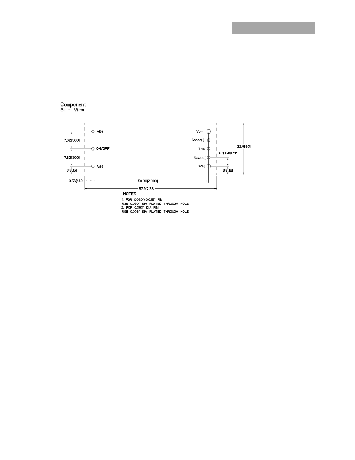
Mechanical Outline for Through-Hole Module
Dimensions are in millimeters and [inches].
Tolerances: x.x mm
x.xx mm
Top
#
View
0.5 mm [x.xx in. 0.02 in.] (Unless otherwise indicated)
0.25 mm [x.xxx in 0.010 in.]
#Top side label includes GE name, product designation and date code.
Side
View
Bottom
View
* For optional pin lengths, see Table 2 Device Options and Coding Scheme
May 15, 2013 ©2012 General Electric Company. All rights reserved. Page 11
Page 12
GE
Data Sheet
EVK011A0B Series (Eighth-Brick) DC-DC Converter Power Modules
36–60Vdc Input; 12.0Vdc Output; 11A Output Current
Recommended Pad Layout
Dimensions are in millimeters and [inches].
Tolerances: x.x mm
x.xx mm
0.5 mm [x.xx in. 0.02 in.] (Unless otherwise indicated)
0.25 mm [x.xxx in 0.010 in.]
TH Recommended Pad Layout (Component Side View)
May 15, 2013 ©2012 General Electric Company. All rights reserved. Page 12
Page 13
GE
Data Sheet
EVK011A0B Series (Eighth-Brick) DC-DC Converter Power Modules
36–60Vdc Input; 12.0Vdc Output; 11A Output Current
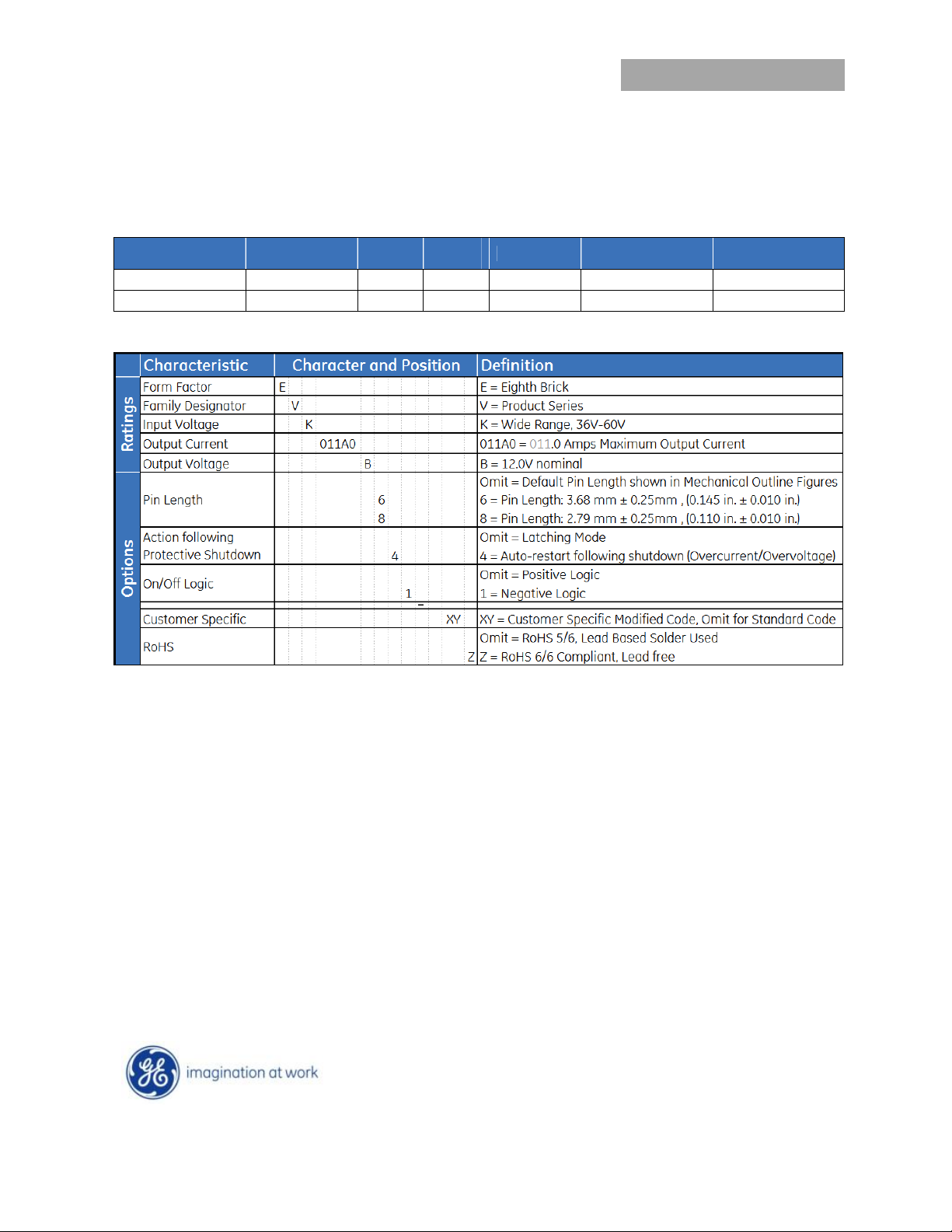
Ordering Information
Please contact your GE Sales Representative for pricing, availability and optional features.
Table 1. Device Codes
Product Codes Input Voltage
EVK011A0B41Z 48V (36-60Vdc) 12V 11A Negative Through hole 150027164
EVK011A0B641Z 48V (36-60Vdc) 12V 11A Negative Through hole 150030268
Table 2. Device Options and Coding Scheme
Output
Voltage
Output
Current
On/Off Logic
Connector
Type
Comcodes
Contact Us
For more information, call us at
USA/Canada:
+1 888 546 3243, or +1 972 244 9288
Asia-Pacific:
+86.021.54279977*808
Europe, Middle-East and Africa:
+49.89.878067-280
India:
May 15, 2013 ©2012 General Electric Company. All rights reserved. Version 1.1
+91.80.28411633
www.ge.com/powerelectronics
 Loading...