

Page 1
Data Sheet
October 5, 2013
EQW010-040 Series (Eighth-Brick) DC-DC Converter Power Modules
36–75Vdc Input; 1.0 to 12.0Vdc Output; 10 to 40A Output Current
RoHS Compliant
Applications
Distributed power architectures
Wireless networks
Access and optical network Equipment
Enterprise Networks
Latest generation IC’s (DSP, FPGA, ASIC) and
Microprocessor powered applications
Options
Negative Remote On/Off logic
Over current/Over temperature/Over voltage
protections (Auto-restart)
Heat plate versions (-C, -H)
Surface Mount version (-S)
Description
The EQW010/040 series DC-DC converters are designed to provide up to 40A output current in an industry standard
eighth brick package. These DC-DC converters operate over an input voltage range of 36 to 75 Vdc and provide a
single, precisely-regulated output. The output is isolated from the input, allowing versatile polarity configurations and
grounding connections. Built in filtering for both the input and output minimizes the need for external filtering.
* UL is a re gistered trademark of Underwriters Laboratories, Inc.
†
CSA is a reg istered trademark of Canadian Standards Associat ion.
‡
VDE is a trademark of Verband Deutscher Elektrotechniker e.V.
§
This product is intended for integration into end-us er equipment
** ISO is a registered trademark of the International Orga nization of Standards
Features
Compliant to RoHS EU Directive 2002/95/EC
Compatible in a Pb-free or SnPb reflow environment
High efficiency – 92% at 3.3V full load
Industry standard, DOSA compliant, Eighth brick
footprint
57.9mm x 22.9mm x 8.5mm
(2.28in x 0.9in x 0.335in)
Wide Input voltage range: 36-75 Vdc
Tightly regulated output
Constant switching frequency
Positive Remote On/Off logic
Input under/over voltage protection
Output overcurrent/voltage protection
Over-temperature protection
Remote sense
No minimum load required
No reverse current during output shutdown
Output Voltage adjust: 80% to 110% of V
Operating temperature range (-40°C to 85°C)
UL* 60950-1Recognized, CSA
03 Certified, and VDE
‡
0805:2001-12 (EN60950-1)
Licensed
CE mark meets 73/23/EEC and 96/68/EEC
directives
§
Meets the voltage and current requirements for
ETSI 300-132-2 and complies with and licensed for
Basic insulation rating per EN60950-1
**
ISO
9001 and ISO 14001 certified manufacturing
facilities
Document No: DS06-112 ver. 1.27
PDF name: EQW010-040 Series.pdf
o,nom
†
C22.2 No. 60950-1-
Page 2

Data Sheet
October 5, 2013
36 – 75Vdc Input; 1.0 to 12.0Vdc Output; 10 to 40A Output Current
EQW010-040 Series Power Modules
Absolute Maximum Ratings
Stresses in excess of the absolute maximum ratings can cause permanent damage to the device. These are
absolute stress ratings only, functional operation of the device is not implied at these or any other conditions in
excess of those given in the operations sections of the data sheet. Exposure to absolute maximum ratings for
extended periods can adversely affect the device reliability.
Parameter Device Symbol Min Max Unit
Input Voltage
Continuous All V
Transient (100 ms) All V
Operating Ambient Temperature All T
IN
IN,trans
A
-0.3 80 Vdc
-0.3 100 Vdc
-40 85 °C
(see Thermal Considerations section)
Storage Temperature All T
I/O Isolation voltage (100% factory Hi-Pot tested) All
stg
-55 125 °C
1500 Vdc
Electrical Specifications
Unless otherwise indicated, specifications apply over all operating input voltage, resistive load, and temperature
conditions.
Parameter Device Symbol Min Typ Max Unit
Operating Input Voltage All VIN 36 48 75 Vdc
Maximum Input Current All, except B I
(VIN= V
IN, min
to V
IN, max
, IO=I
) B I
O, max
Input No Load Current All I
(VIN = V
, IO = 0, module enabled)
IN, nom
Input Stand-by Current All I
(VIN = V
, module disabled)
IN, nom
IN,max
IN,max
IN,No load
IN,stand-by
3.2 3.5 Adc
3.4 3.7 Adc
75 mA
22 mA
Inrush Transient All I2t 0.5 A2s
Input Reflected Ripple Current, peak-to-peak
(5Hz to 20MHz, 1μH source impedance; V
V
= I
IN, max, IO
; See Test configuration section)
Omax
IN, min
to
All 20 mA
p-p
Input Ripple Rejection (120Hz) All 50 dB
CAUTION: This power module is not internally fused. An input line fuse must always be used.
This power module can be used in a wide variety of applications, ranging from simple standalone operation to an
integrated part of sophisticated power architectures. To preserve maximum flexibility, internal fusing is not included,
however, to achieve maximum safety and system protection, always use an input line fuse. The safety agencies
require a time-delay fuse with a maximum rating of 8 A (see Safety Considerations section). Based on the
information provided in this data sheet on inrush energy and maximum dc input current, the same type of fuse with a
lower rating can be used. Refer to the fuse manufacturer’s data sheet for further information.
LINEAGE POWER 2
Page 3

Data Sheet
A
A
October 5, 2013
36 – 75Vdc Input; 1.0 to 12.0Vdc Output; 10 to 40A Output Current
EQW010-040 Series Power Modules
Electrical Specifications (continued)
Parameter Device Symbol Min Typ Max Unit
Nominal Output Voltage Set-point B V
VIN=V
IN, min
, IO=I
, TA=25°C) A V
O, max
F V
G V
Y V
M V
P V
S1R0 V
O, set
O, set
O, set
O, set
O, set
O, set
O, set
O, set
Output Voltage
(Over all operating input voltage, resistive load,
All V
O
and temperature conditions until end of life)
Output Regulation
Line (VIN=V
IN, min
to V
) B, A, F, G
IN, max
Y, M, P, S1R0 5 mV
Load (IO=I
O, min
to I
O, max
)
B, A, F, G
0.2 % V
Y, M, P, S1R0 5 mV
Temperature (T
ref=TA, min
to T
) All
A, max
Output Ripple and Noise on nominal output
(VIN=V
IN, nom
,IO= I
O, max
, TA=T
, min
to T
)
, max
RMS (5Hz to 20MHz bandwidth) B
Peak-to-Peak (5Hz to 20MHz bandwidth) B
RMS (5Hz to 20MHz bandwidth) All, except B
Peak-to-Peak (5Hz to 20MHz bandwidth) All, except B
External Capacitance B C
A C
F, G, Y, M, P,
S1R0
Output Current B I
C
O, max
O, max
O, max
o
A Io 0
F Io 0
G Io 0
Y, M, P, S1R0 Io 0
Output Current Limit Inception (Hiccup Mode ) All, except G
(VO= 90% of V
Output Short-Circuit Current
(VO≤250mV) ( Hiccup Mode )
) G
O, set
All I
I
O, lim
I
O, lim
O, s/c
Efficiency B η 93.0 %
VIN= V
IO=I
, TA=25°C A η 91.7 %
IN, nom
= V
O, max , VO
F η 92.0 %
O,set
G η 89.8 %
Y η 88.3 %
M η 87.1 %
P η 85.0 %
S1R0 η 83.2 %
Switching Frequency All f
* Note: For 1.0VO (S1R0) and 1.2 VO (P) device codes, external capacitance, CO, should be 1000uF minimum to achieve monotonic start-up with
very light load (≤ 2Amp).
sw
11.76 12.0 12.24 V
4.90 5.0 5.10 V
3.23 3.3 3.37 V
2.45 2.5 2.55 V
1.76 1.8 1.84 V
1.47 1.5 1.53 V
1.18 1.2 1.22 V
0.98 1.0 1.02 V
-3.0
0
0
0*
0
+3.0 % V
0.2 % V
1.0 % V
30 mV
100 mV
25 mV
75 mV
1,500 μF
10,000 μF
20,000 μF
10 Adc
20 Adc
30 Adc
35 Adc
40 Adc
105 115 130
103 115 130
130 150 A
% I
% I
dc
dc
dc
dc
dc
dc
dc
dc
O, set
O, set
O, set
O, set
rms
pk-pk
rms
pk-pk
rms
o
o
420 kHz
LINEAGE POWER 3
Page 4
Data Sheet
October 5, 2013
36 – 75Vdc Input; 1.0 to 12.0Vdc Output; 10 to 40A Output Current
EQW010-040 Series Power Modules
Electrical Specifications (continued)
Parameter Device Symbol Min Typ Max Unit
Dynamic Load Response
(dIo/dt=0.1A/s; VIN = V
IN, nom
; TA=25°C)
Load Change from Io= 50% to 75% or 25% to
50% of Io,max;
Peak Deviation All V
Settling Time (Vo<10% peak deviation)
(dIo/dt=1A/s; VIN = V
IN, nom
; TA=25°C)
Load Change from Io= 50% to 75% or 25% to
50% of Io,max;
All t
Peak Deviation All V
Settling Time (Vo<10% peak deviation)
All t
pk
s
pk
s
3
200
s
% V
5
200
s
% V
Isolation Specifications
Parameter Device Symbol Min Typ Max Unit
Isolation Capacitance All C
Isolation Resistance All R
I/O Isolation Voltage (100% factory Hi-pot tested) All All
iso
iso
10
1000
1500 Vdc
pF
MΩ
O, set
O, set
General Specifications
Parameter Device Symbol Min Typ Max Unit
Calculated Reliability based upon Telcordia SR332 Issue 2: Method
=40°C, airflow = 200 lfm, 90% confidence)
T
A
I Case 3 (I
=80%I
O
O, max
,
B FIT 334 10
A-S FIT 290 109/Hours
F FIT 328 109/Hours
Y FIT 302 109/Hours
B MTBF 2,997,896 Hours
A-S MTBF 3,451,558 Hours
F MTBF 3,051,626 Hours
Y MTBF 3,312,888 Hours
Weight All
20.5
(0.72)
9
(oz.)
/Hours
g
LINEAGE POWER 4
Page 5

Data Sheet
October 5, 2013
36 – 75Vdc Input; 1.0 to 12.0Vdc Output; 10 to 40A Output Current
EQW010-040 Series Power Modules
Feature Specifications
Unless otherwise indicated, specifications apply over all operating input voltage, resistive load, and temperature
conditions. See Feature Descriptions for additional information.
Parameter Device Symbol Min Typ Max Unit
Remote On/Off Signal Interface
(VIN=V
Signal referenced to V
Negative Logic: device code suffix “1”
Logic Low = module On, Logic High = module Off
Positive Logic: No device code suffix required
Logic Low = module Off, Logic High = module On
Logic Low - Remote On/Off Current All I
Logic Low - On/Off Voltage All V
Logic High Voltage – (Typ = Open Collector) All V
Logic High maximum allowable leakage current All I
Turn-On Delay and Rise Times
(IO=I
Case 1: On/Off input is set to Logic Low (Module
ON) and then input power is applied (T
instant at which V
Case 2: Input power is applied for at least 1 second
and then the On/Off input is set from OFF to ON (T
from instant at which V
Output voltage Rise time (time for Vo to rise from 10%
of V
Output voltage Rise time (time for Vo to rise from 10%
of V
Output voltage overshoot – Startup
IO= I
Remote Sense Range
(Max voltage drop is 0.5V) B*, A, F V
Output Voltage Adjustment Range All* 80 110 % V
Output Overvoltage Protection
A V
F V
G V
Y V
M V
P V
S1R0 V
Input Undervoltage Lockout All V
Turn-on Threshold
Turn-off Threshold
Hysterisis 1.5 2
Input Overvoltage Lockout All V
Turn-on Threshold
Turn-off Threshold
Hysterisis 2 3.5
* Note: 12.0VO (B) device codes have an adaptable extended Turn-On Delay interval, T
when a 12V
to normal; or 2) toggling the on/off signal from on to off and back to on without removing the input voltage. The normal Turn-On Delay interval, T
as specified for All Devices, will occur whenever a 12V
12.0V
to V
IN, min
O, max , VIN=VIN, nom, TA
to 90% of V
o,set
to 90% of V
o,set
; VIN=V
O, max
; open collector or equivalent,
IN, max
terminal)
IN-
on/off
on/off
on/off
on/off
-0.7
5 V
1.0 mA
1.2 Vdc
10 μA
= 25 oC)
T
delay
T
delay
T
delay
T
delay
rise
rise
V
SENSE
SENSE
O, limit
O, limit
O, limit
O, limit
O, limit
O, limit
O, limit
O, limit
UVLO
―
―
―
―
20
25
5
25
25
30
10
30
― 8 12
― 8 12
― 3 % V
0.25 Vdc
10 % V
14
5.7
3.8
2.9
2.3
1.8
1.4
1.2
16 Vdc
6.5 Vdc
4.6 Vdc
3.4 Vdc
2.6 Vdc
2.2 Vdc
1.6 Vdc
1.4 Vdc
30 34.5 36 Vdc
30 32
= V
until Vo=10% of V
IN, min
IN=VIN, min
until VO = 10% of V
)
with max ext capacitance)
, TA = 25 oC
IN, max
IN, min
IN
o, set
o, set
to V
delay
from
O,set
)
delay
O, set
All
B*
All
=
B*
).
All T
All T
All
G, Y, M,
P, S1R0
B V
OVLO
80
75 79 83 Vdc
, as specified for B* devices. The extended T
module restarts following either 1) the rapid cycling of Vin from normal levels to less than the Input Undervoltage Lockout and then back
O
module restarts with input voltage removed from the module for the preceding 1 second.
(B) also achieves +10% V
O
Remote Sense drop or trim up to 110% V
O, set
O
delay
only above Vin = 40Vdc.
O, set
will occur
delay
dc
msec
msec
msec
msec
msec
msec
O, set
O, set
O, set
Vdc
Vdc
V
dc
Vdc
,
delay
LINEAGE POWER 5
Page 6
Data Sheet
October 5, 2013
36 – 75Vdc Input; 1.0 to 12Vdc Output; 10 to 40A Output Current
EQW010-040 Series Power Modules
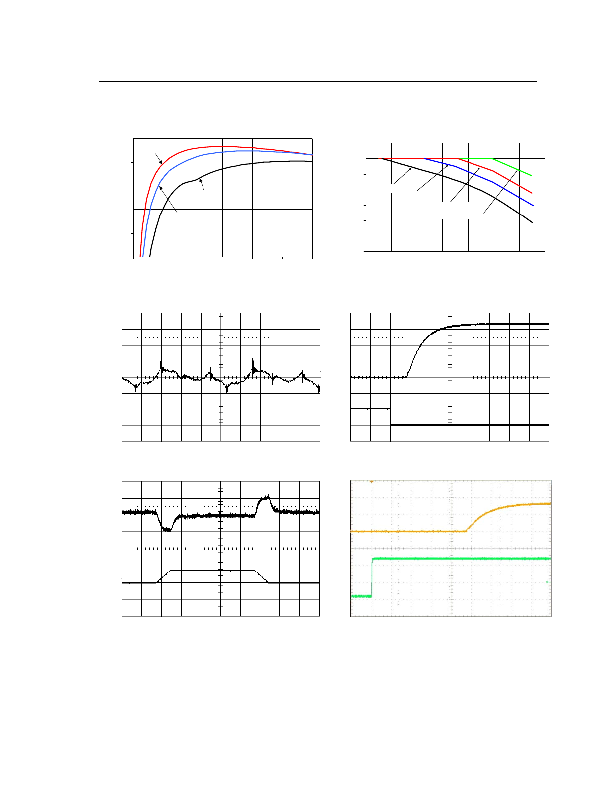
Characteristic Curves
The following figures provide typical characteristics for the EQW010A0B (12V, 10A) at 25oC. The figures are
identical for either positive or negative remote On/Off logic.
95
12
90
85
Vin = 36V
Vin = 48V
80
Vin = 75V
75
EFFICIENCY, (%)
70
10
8
6
4
2
0
20 30 40 50 60 70 80 90
OUTPUT CURRENT, Io (A)
NC
0.5 m/s
(100 LFM)
1.0 m/s
(200 LFM)
2.0 m/s
(400 LFM)
OUTPUT CURRENT, IO (A) AMBIENT TEMPERATURE, TA OC
Figure 1. Converter Efficiency versus Output Current. Figure 4. Derating Output Current versus Local
Ambient Temperature and Airflow (direc tio n sh own
in Figure 63).
(V) (5V/div)
O
(V) (50mV/div)
O
V
OUTPUT VOLTAGE
TIME, t (1s/div)
Figure 2. Typical output ripple and noise (V
I
o = Io,max).
IN = VIN,NOM,
(V) (5V/div) V
On/off
On/Off VOLTAGE OUTPUT VOLTAGE
V
TIME, t (5ms/div)
Figure 5. Typical Start-up Using Remote On/Off,
negative logic version, (VIN = VIN,NOM, Io = Io,max) [where
input voltage has not been applied in the previous 1 second, see
page 5].
(V) (5V/div)
(V) (200mV/div)
O
Io (A) (5A/div) V
OUTPUT CURRENT OUTPUT VOLTAGE
TIME, t (0.1 ms /div) TIME, t (5ms/div)
Figure 3. Transient Response to Dynamic Load
Change from 75% to 50% to 75% of full load.
O
(V) (50V/div) V
IN
INPUT VOLTAGE OUTPUT VOLTAGE
V
Figure 6. Typical Start-up Using Input Voltage, (VIN
= V
IN,NOM, Io = Io,max) [where input voltage has not been applied
in the previous 1 second , see page 5].
LINEAGE POWER 6
Page 7
Data Sheet
October 5, 2013
36 – 75Vdc Input; 1.0 to 12.0Vdc Output; 10 to 40A Output Current
EQW010-040 Series Power Modules
Characteristic Curves
The following figures provide typical characteristics for the EQW020A0A (5.0V, 20A) at 25oC. The figures are
identical for either positive or negative remote On/Off logic.
95
25
90
85
80
75
70
EFFICIENCY, (%)
0 5 10 15 20
Vin = 48V
Vin = 36V
Vin = 75V
20
15
10
5
0
OUTPUT CURRENT, Io (A)
20 30 40 50 60 70 80 90
NC
0.5 m/s
(100 LFM)
1.0 m/s
(200 LFM)
2.0 m/s
(400 LFM)
OUTPUT CURRENT, IO (A) AMBIENT TEMPERATURE, TA OC
Figure 7. Converter Efficiency versus Output Current. Figure 10. Derating Output Current versus Local
Ambient Temperature and Airflow (direc tio n sh own in
Figure 63).
(V) (2V/div)
O
(V) (20mV/div)
O
V
OUTPUT VOLTAGE
TIME, t (1s/div)
Figure 8. Typical output ripple and noise (V
I
o = Io,max).
IN = VIN,NOM,
(V) (5V/div) V
On/Off
On/Off VOLTAGE OUTPUT VOLTAGE
V
TIME, t (5ms/div)
Figure 11. Typical Start-up Using Remote On/Off,
negative logic version shown (VIN = VIN,NOM, Io = Io,max).
(V) (100mV/div)
O
Io(A) (10A/div) V
VOLTAGE
TIME, t (0.1ms/div) TIME, t (4ms/div)
Figure 9. Transient Response to Dynamic Load
Change from 50% to 75% to 50% of full load.
(V) (2V/div)
O
(V) (20V/div) V
IN
INPUT VOLTAGE OUTPUT VOLTAGE
V
Figure 12. Typical Start-up Using Input Voltage (VIN =
V
IN,NOM, Io = Io,max).
LINEAGE POWER 7
Page 8
Data Sheet
October 5, 2013
36 – 75Vdc Input; 1.0 to 12.0Vdc Output; 10 to 40A Output Current
EQW010-040 Series Power Modules
Characteristic Curves (continued)
The following figures provide typical characteristics for the EQW030A0F (3.3V, 30A) at 25oC. The figures are
identical for either positive or negative remote On/Off logic.
95
Vin = 36V
90
85
80
75
EFFICIENCY, (%)
70
0 5 10 15 20 25 30
Vin = 75V
Vin = 48V
OUTPUT CURRENT, IO (A) AMBIENT TEMPERATURE, TA OC
Figure 13. Converter Efficiency versus Output
Current.
35
30
25
20
15
10
5
0
OUTPUT CURRENT, Io (A)
NC
0.5 m/s
(100 LFM)
20 30 40 50 60 70 80 90
1.0 m/s
(200 LFM)
2.0 m/s
(400 LFM)
Figure 16. Derating Output Current versus Local
Ambient Temperature and Airflow (direc tio n sh own in
Figure 63).
(V) (20mV/div)
O
V
OUTPUT VOLTAGE
TIME, t (1s/div)
Figure 14. Typical outp u t ripp l e and noise (V
V
IN,NOM, Io = Io,max).
(V) (100mV/div)
O
Io(A) (10A/div) V
VOLTAGE
TIME, t (0.1ms/div) TIME, t (4ms/div)
IN =
Figure 15. Transient Respon se to Dynamic Load
Change from 50% to 75% to 50% of full load.
(V) (1V/div)
On/off
(V) (5V/div) V
O
V
On/Off VOLTAGE OUTPUT VOLTAGE
TIME, t (5ms/div)
Figure 17. Typical Start-up Using Remote On/Off,
negative logic version shown (VIN = VIN,NOM, Io = Io,max).
(V) (2V/div)
IN
(V) (20V/div) V
O
V
INTPUT VOLTAGE OUTPUT VOLTAGE
Figure 18. Typical Start-up Using Input Voltage (VIN =
V
IN,NOM, Io = Io,max).
LINEAGE POWER 8
Page 9
Data Sheet
October 5, 2013
36 – 75Vdc Input; 1.0 to 12.0Vdc Output; 10 to 40A Output Current
EQW010-040 Series Power Modules
Characteristic Curves (continued)
The following figures provide typical characteristics for the EQW035A0G (2.5V, 35A) at 25oC. The figures are
identical for either positive or negative remote On/Off logic.
95
Vin = 36V
90
85
80
75
70
EFFICIENCY, (%)
0 5 10 15 20 25 30 35
Vin = 48V
Vin = 75V
OUTPUT CURRENT, IO (A) AMBIENT TEMPERATURE, TA OC
Figure 19. Converter Efficiency versus Output
Current.
40
35
30
25
20
15
10
5
20 30 40 50 60 70 80 90
OUTPUT CURRENT, Io (A)
NC
0.5 m/s
(100 LFM)
1.0 m/s
(200 LFM)
2.0 m/s
(400 LFM)
Figure 22. Derating Output Current versus Local
Ambient Temperature and Airflow (direc tio n sh own
in Figure 63).
(V) (20mV/div)
O
V
OUTPUT VOLTAGE
TIME, t (1s/div)
Figure 20. Typical outp u t ripp l e and noise (V
V
IN,NOM, Io = Io,max).
(V) (100mV/div)
O
Io (A) (10A/div) V
VOLTAGE
TIME, t (0.1ms/div) TIME, t (4ms/div)
IN =
Figure 21. Transient Respon se to Dynamic Load
Change from 50% to 75% to 50% of full load.
(V) (1V/div)
O
(V) (5V/div) V
On/Off
On/Off VOLTAGE OUTPUT VOLTAGE
V
TIME, t (5ms/div)
Figure 23. Typical Start-up Using Remote On/Off,
negative logic version shown (VIN = VIN,NOM, Io =
I
o,max).
(V) (1.0V/div)
O
(V) (20V/div) V
IN
INPUT VOLTAGE OUTUT VOLTAGE
V
Figure 24. Typical Start-up Using Input Voltage (VIN
= V
IN,NOM, Io = Io,max).
LINEAGE POWER 9
Page 10

Data Sheet
October 5, 2013
36 – 75Vdc Input; 1.0 to 12.0Vdc Output; 10 to 40A Output Current
EQW010-040 Series Power Modules
Characteristic Curves (continued)
The following figures provide typical characteristics for the EQW040A0Y (1.8V, 40A) at 25oC. The figures are
identical for either positive or negative remote On/Off logic.
95
Vin = 36V
Vin = 75V
Vin = 48V
0 5 10 15 20 25 30 35 40
EFFICIENCY, (%)
90
85
80
75
70
OUTPUT CURRENT, IO (A) AMBIENT TEMPERATURE, TA OC
Figure 25. Converter Efficiency versus Output
Current.
45
40
35
30
NC
25
20
15
0.5 m/s
(100 LFM)
1.0 m/s
(200 LFM)
2.0 m/s
(400 LFM)
10
20 30 40 50 60 70 80 90
OUTPUT CURRENT, Io (A)
Figure 28. Derating Output Current versus Local
Ambient Temperature and Airflow (direc tio n sh own
in Figure 63).
(V) (20mV/div)
O
V
OUTPUT VOLTAGE
TIME, t (1s/div)
Figure 26. Typical outp u t ripp l e and noise (V
V
IN,NOM, Io = Io,max).
(V) (50mV/div)
O
Io (A) (10A/div) V
OUTPUT CURRENT OUTPUT VOLTAGE
TIME, t (0.1ms/div) TIME, t (4ms/div)
IN =
Figure 27. Transient Respon se to Dynamic Load
Change from 50% to 75% to 50% of full load.
(V) (1.0V/div)
O
(V) (5V/div) V
On/off
V
On/Off VOLTAGE OUTPUT VOLTAGE
TIME, t (10ms/div)
Figure 29. Typical Start-up Using Remote On/Off,
negative logic version shown (VIN = VIN,NOM, Io =
I
o,max).
(V) (1.0V/div)
O
(V) (20V/div) V
IN
INPUT VOLTAGE OUTPUT VOLTAGE
V
Figure 30. Typical Start-up Using Input Voltage (VIN
= V
IN,NOM, Io = Io,max).
LINEAGE POWER 10
Page 11

Data Sheet
October 5, 2013
36 – 75Vdc Input; 1.0 to 12.0Vdc Output; 10 to 40A Output Current
EQW010-040 Series Power Modules
Characteristic Curves (continued)
The following figures provide typical characteristics for the EQW040A0M (1.5V, 40A) at 25oC. The figures are
identical for either positive or negative remote On/Off logic.
90
Vin = 36V
85
80
Vin = 48V
75
EFFICIENCY, (%)
70
0 5 10 15 20 25 30 35 40
Vin = 75V
OUTPUT CURRENT, IO (A) AMBIENT TEMPERATURE, TA OC
Figure 31. Converter Efficiency versus Output
Current.
45
40
35
30
25
20
15
10
OUTPUT CURRENT, Io (A)
20 30 40 50 60 70 80 90
NC
0.5 m/s
(100 LFM)
1.0 m/s
(200 LFM)
2.0 m/s
(400 LFM)
Figure 34. Derating Output Current versus Local
Ambient Temperature and Airflow (direc tio n sh own
in Figure 63).
(V) (20mV/div)
O
V
OUTPUT VOLTAGE
TIME, t (1s/div)
Figure 32. Typical outp u t ripp l e and noise (V
V
IN,NOM, Io = Io,max).
(V) (50mV/div)
O
Io (A) (10A/div) V
VOLTAGE
TIME, t (0.1ms/div) TIME, t (4ms/div)
IN =
Figure 33. Transient Respon se to Dynamic Load
Change from 50% to 75% to 50% of full load.
(V) (0.5V/div)
O
(V) (5.0V/div) V
On/Off
V
On/Off VOLTAGE OUTPUT VOLTAGE
TIME, t (5ms/div)
Figure 35. Typical Start-up Using Remote On/Off,
negative logic version shown (VIN = VIN,NOM, Io =
I
o,max).
(V) (0.5V/div)
O
(V) (20.0V/div) V
I
INPUT VOLTAGE OUTPUT VOLTAGE
V
Figure 36. Typical Start-up Using Input Voltage (VIN
= V
IN,NOM, Io = Io,max).
LINEAGE POWER 11
Page 12

Data Sheet
October 5, 2013
36 – 75Vdc Input; 1.0 to 12.0Vdc Output; 10 to 40A Output Current
EQW010-040 Series Power Modules
Characteristic Curves (continued)
The following figures provide typical characteristics for the EQW040A0P (1.2V, 40A) at 25oC. The figures are
identical for either positive or negative remote On/Off logic.
90
Vin = 36V
85
80
Vin = 48V
75
70
EFFICIENCY, (%)
0 5 10 15 20 25 30 35 40
Vin = 75V
OUTPUT CURRENT, IO (A) AMBIENT TEMPERATURE, TA OC
Figure 37. Converter Efficiency versus Output
Current.
45
40
35
30
25
20
15
10
OUTPUT CURRENT, Io (A)
NC
0.5 m/s
(100 LF M)
20 30 40 50 60 70 80 90
1.0 m/s
(200 LFM)
2.0 m/s
(400 LFM)
Figure 40. Derating Output Current versus Local
Ambient Temperature and Airflow (direc tio n sh own
in Figure 63).
(V) (20mV/div)
O
V
OUTPUT VOLTAGE
TIME, t (1s/div)
Figure 38. Typical outp u t ripp l e and noise (V
V
IN,NOM, Io = Io,max).
(V) (50mV/div)
O
Io (A) (10A/div) V
OUTPUT CURRENT OUTPUT VOLTAGE
TIME, t (0.1ms/div) TIME, t (4ms/div)
IN =
Figure 39. Transient Respon se to Dynamic Load
Change from 50% to 75% to 50% of full load.
(V) (0.5V/div)
On/off
(V) (5.0V/div) V
O
V
On/Off VOLTAGE OUTPUT VOLTAGE
TIME, t (5ms/div)
Figure 41. Typical Start-up Using Remote On/Off,
negative logic version shown (VIN = VIN,NOM, Io =
I
o,max).
(V) (0.5V/div)
IN
(V) 20.0V/div) V
O
INPUT VOLTAGE OUTUT VOLTAGE
V
Figure 42. Typical Start-up Using Input Voltage (VIN
= V
IN,NOM, Io = Io,max).
LINEAGE POWER 12
Page 13

Data Sheet
October 5, 2013
36 – 75Vdc Input; 1.0 to 12.0Vdc Output; 10 to 40A Output Current
EQW010-040 Series Power Modules
Characteristic Curves (continued)
The following figures provide typical characteristics for the EQW040A0S1R0 (1.0V, 40A) at 25oC. The figures are
identical for either positive or negative remote On/Off logic.
90
Vin = 36V
85
80
Vin = 75V
EFFICIENCY, (%)
75
Vin = 48V
70
0 5 10 15 20 25 30 35 40
OUTPUT CURRENT, IO (A) AMBIENT TEMPERATURE, TA OC
Figure 43. Converter Efficiency versus Output
Current.
45
40
35
30
25
20
15
20 30 40 50 60 70 80 90
OUTPUT CURRENT, Io (A)
NC
0.5 m/s
(100 LFM)
1.0 m/s
(200 LFM)
2.0 m/s
(400
Figure 46. Derating Output Current versus Local
Ambient Temperature and Airflow (direc tio n sh own
in Figure 63).
(V) (20mV/div)
O
V
OUTPUT VOLTAGE
TIME, t (1s/div)
Figure 44. Typical outp u t ri pp le and noise (V
V
IN,NOM, Io = Io,max).
(V) (50mV/div)
O
Io (A) (20A/div) V
OUTPUT CURRENT OUTPUT VOLTAGE
TIME, t (0.1ms/div) TIME, t (4ms/div)
IN =
Figure 45. Transient Response to Dynamic Load
Change from 50% to 75% to 50% of full load.
(V) (0.5V/div)
On/off
(V) (3.0V/div) V
O
V
On/Off VOLTAGE OUTPUT VOLTAGE
TIME, t (5ms/div)
Figure 47. Typical Start-up Using Remote On/Off,
negative logic version shown (VIN = VIN,NOM, Io =
I
o,max).
(V) (0.5V/div)
IN
(V) (20.0V/div) V
O
INPUT VOLTAGE OUTPUT VOLTAGE
V
Figure 48. Typical Start-up Using Input Voltage (VIN
= V
IN,NOM, Io = Io,max).
LINEAGE POWER 13
Page 14

Data Sheet
October 5, 2013
36 – 75Vdc Input; 1.0 to 12.0Vdc Output; 10 to 40A Output Current
EQW010-040 Series Power Modules
Characteristic Curves (continued)
Derating Output Current versus Local Ambient Temperature and Airflow (direction shown in Figure 63) for heat plate
versions (-C, -H).
12
45
10
8
6
4
2
20 30 40 50 60 70 80 90
OUTPUT CURRENT, Io (A)
NC
0.5 m/s
(100 LFM)
1.0 m/s
(200 LFM)
2.0 m/s
(400 LFM)
40
35
30
25
20
15
20 30 40 50 60 70 80 90
OUTPUT CURRENT, Io (A)
NC
(100 LFM)
0.5 m/s
1.0 m/s
(200 LF M)
2.0 m/s
(400 LFM)
AMBIENT TEMPERATURE, TA OC AMBIENT TEMPERATURE, TA OC
Figure 49. EQW010A0B-C/H, (12.0 V, 10A ). Figure 53. EQW040A0Y-C/H, (1.8 V, 40A).
25
20
15
10
5
20 30 40 50 60 70 80 90
OUTPUT CURRENT, Io (A)
NC
0.5 m/s
(100 LFM)
1.0 m/s
(200 LFM)
2.0 m/s
(400 LFM)
AMBIENT TEMPERATURE, TA OC AMBIENT TEMPERATURE, TA OC
45
40
35
30
25
20
15
20 30 40 50 60 70 80 90
OUTPUT CURRENT, Io (A)
NC
0.5 m/s
(100 LFM)
1.0 m/s
(200 LFM)
2.0 m/s
(400 LFM)
Figure 50. EQW020A0A -C/ H, (5.0V, 20A). Figure 54. EQW040A0M-C/H, (1.5V, 40A).
35
30
25
20
15
10
5
0
20 30 40 50 60 70 80 90
OUTPUT CURRENT, Io (A)
NC
0.5 m/s
(100 LFM)
1.0 m/s
(200 LFM)
2.0 m/s
(400 LFM)
AMBIENT TEMPERATURE, TA OC AMBIENT TEMPERATURE, TA OC
45
40
35
30
25
20
15
20 30 40 50 60 70 80 90
OUTPUT CURRENT, Io (A)
NC
0.5 m/s
(100 LFM)
1.0 m/s
(200 LFM)
2.0 m/s
(400 LFM)
Figure 51. EQW030A0F-C/H, (3 .3 V, 30A). Figure 55. EQW040A0P-C/H, (1.2V, 40A).
40
35
30
25
20
15
10
20 30 40 50 60 70 80 90
OUTPUT CURRENT, Io (A)
NC
0.5 m/s
(100 LFM)
1.0 m/s
(200 LFM)
2.0 m/s
(400 LFM)
AMBIENT TEMPERATURE, TA OC AMBIENT TEMPERATURE, TA OC
45
40
35
30
25
20
15
20 30 40 50 60 70 80 90
OUTPUT CURRENT, Io (A)
NC
0.5 m/s
(100 LFM)
1.0 m/s
(200 LFM)
2.0 m/s
(400 LFM)
Figure 52. EQW035A0G-C/H, (2.5 V, 35A). Figure 56. EQW040A0S-C/H, (1.0V, 40A).
LINEAGE POWER 14
Page 15

Data Sheet
October 5, 2013
36 – 75Vdc Input; 1.0 to 12.0Vdc Output; 10 to 40A Output Current
Test Configurations
SCOPE
Vout+
Vout-
CURRENT PROBE
33μF
RESISTIVE
LOAD
V
O
x 100 %
Vin+
Vin-
R
contactRdistribution
R
contactRdistribution
R
LOAD
TO OSCILLOSCOPE
L
TEST
12μH
CS 220μF
BATTERY
NOTE: Measure input reflected ripple current with a simulated
E.S.R.<0.1
@ 20°C 100kHz
source inductance (L
possible battery impedance. Measure current as shown
above.
) of 12μH. Capacitor CS offsets
TEST
Figure 57. Input Reflected Ripple Current Test
Setup.
COPPER STRIP
V
(+)
O
V O ( – )
NOTE: All voltage measurements to be take n at the module
0.01uF
terminals, as shown above. If sockets are used then
Kelvin connections are required at the module terminals
to avoid measurement errors due to socket contact
resistance.
0.1uF
GROUND PLANE
10uF
Figure 58. Output Ripple and Noise Test Setup.
R
R
contact
distribution
R
R
contact
distribution
NOTE: All voltage measurements to be taken at t he module
terminals, as shown above. If sockets are used then
Kelvin connections are required at the module terminals
to avoid measurement errors due to socket contact
resistance.
Vin+
V
IN
Vin-
Figure 59. Output Voltage and Efficiency Test
Setup.
. I
V
O
Efficiency
=
VIN. I
O
IN
EQW010-040 Series Power Modules
Design Considerations
Input Filt ering
The power module should be connected to a low
ac-impedance source. Highly inductive source
impedance can affect the stability of the power
module. For the test configuration in Figure 57 a 33μF
electrolytic capacitor (ESR<0.1 at 100kHz),
mounted close to the power module helps ensure the
stability of the unit. Consult the factory for further
application guidelines.
Output Filtering
For 1.0V to 1.2V output voltage modules, an external
capacitance of 1000uF is recommended to achieve
monotonic start-up with very light load (≤ 2Amp).
Safety Considerations
For safety-agency approval of the system in which the
power module is used, the power module must be
installed in compliance with the spacing and
separation requirements of the end-use safety agency
standard, i.e., UL 60950-1-3, CSA C22.2 No. 6095000, and VDE 0805:2001-12 (IEC60950-1).
If the input source is non-SELV (ELV or a hazardous
voltage greater than 60 Vdc and less than or equal to
75Vdc), for the module’s output to be considered as
meeting the requirements for safety extra-low voltage
(SELV), all of the following must be true:
The input source is to be provided with reinforced
insulation from any other hazardous voltages,
including the ac mains.
One V
The input pins of the module are not operator
Another SELV reliability test is conducted on the
Note: Do not ground either of the input pins of the
The power module has extra-low voltage (ELV)
outputs when all inputs are ELV.
All flammable materials used in the manufacturing of
these modules are rated 94V-0, or tested to the
UL60950 A.2 for reduced thickness.
For input voltages exceeding –60 Vdc but less than or
equal to –75 Vdc, these converters have been
evaluated to the applicable requirements of BASIC
INSULATION between secondary DC MAINS
DISTRIBUTION input (classified as TNV-2 in Europe)
and unearthed SELV outputs.
The input to these units is to be provided with a
maximum 8 A time-delay fuse in the ungrounded lead.
pin and one V
IN
pin are to be
OUT
grounded, or both the input and output pins are
to be kept floating.
accessible.
whole system (combination of supply source and
subject module), as required by the safety
agencies, to verify that under a single fault,
hazardous voltages do not appear at the
module’s output.
module without grounding one of the output
pins. This may allow a non-SELV voltage to
appear between the output pins and ground.
LINEAGE POWER 15
Page 16

Data Sheet
E
October 5, 2013
36 – 75Vdc Input; 1.0 to 12.0Vdc Output; 10 to 40A Output Current
Feature Description
Remote On/Off
Two remote on/off options are available. Positive logic
turns the module on during a logic high voltage on the
ON/OFF pin, and off during a logic low. Negative logic
remote On/Off, device code suffix “1”, turns the
module off during a logic high and on during a logic
low.
Vin+
I
on/off
V
on/off
ON/OFF
Vin-
Figure 60. Remote On/Off Implementation.
To turn the power module on and off, the user must
supply a switch (open collector or equivalent) to
control the voltage (V
terminal and the V
low is 0V ≤ V
≤ 1.2V. The maximum I
on/off
) between the ON/OFF
on/off
(-) terminal (see Figure 60). Logic
IN
logic low is 1mA, the switch should be maintain a
logic low level whilst sinking this current.
During a logic high, the typical maximum V
generated by the module is 15V, and the maximum
allowable leakage current at V
If not using the remote on/off feature:
For positive logic, leave the ON/OFF pin open.
For negative logic, short the ON/OFF pin to V
Remote Sense
Remote sense minimizes the effects of distribution
losses by regulating the voltage at the remote-sense
connections (See Figure 61). The voltage between
the remote-sense pins and the output terminals must
not exceed the output voltage sense range given in
the Feature Specifications table:
[VO(+) – VO(–)] – [SENSE(+) – SENSE(–)] 0.5 V
Although the output voltage can be increased by both
the remote sense and by the trim, the maximum
increase for the output voltage is not the sum of both.
The maximum increase is the larger of either the
remote sense or the trim.
The amount of power delivered by the module is
defined as the voltage at the output terminals
multiplied by the output current. When using remote
sense and trim, the output voltage of the module can
be increased, which at the same output current would
increase the power output of the module. Care should
Vout+
TRIM
Vout-
= 5V is 1μA.
on/off
during a
on/off
on/off
(-).
IN
EQW010-040 Series Power Modules
be taken to ensure that the maximum output power of
the module remains at or below the maximum rated
power (Maximum rated power = Vo,set x Io,max).
SENSE(+)
SENSE(–)
V
I(+)
SUPPLY
CONTACT
RESISTANCE
I
I
VO(+)
I(-)
V
O(–)
V
DISTRIBUTION LOSS
IO
CONTACT AND
Figure 61. Circuit Configuration for remote
sense .
Input Undervoltage Lockout
At input voltages below the input undervoltage lockout
limit, the module operation is disabled. The module
will only begin to operate once the input voltage is
raised above the undervoltage lockout turn-on
threshold, V
UV/ON
.
Once operating, the module will continue to operate
until the input voltage is taken below the undervoltage
turn-off threshold, V
UV/OFF
.
Overtemperature Protection
To provide protection under certain fault conditions,
the unit is equipped with a thermal shutdown circuit.
The unit will shutdown if the thermal reference point
Tref (Figure 63), exceeds 125
o
C (typical), but the
thermal shutdown is not intended as a guarantee that
the unit will survive temperatures beyond its rating.
The module can be restarted by cycling the dc input
power for at least one second or by toggling the
remote on/off signal for at least one second. If the
auto-restart option (4) is ordered, the module will
automatically restart upon cool-down to a safe
temperature.
Output Overvoltage Protection
The output over voltage protection scheme of the
modules has an independent over voltage loop to
prevent single point of failure. This protection feature
latches in the event of over voltage across the output.
Cycling the on/off pin or input voltage resets the
latching protection feature. If the auto-restart option
(4) is ordered, the module will automatically restart
upon an internally programmed time elapsing.
Overcurrent Protection
To provide protection in a fault (output overload)
condition, the unit is equipped with internal
current-limiting circuitry and can endure current
limiting continuously. At the point of current-limit
inception, the unit enters hiccup mode. If the unit is
not configured with auto–restart, then it will latch off
LOAD
LINEAGE POWER 16
Page 17

Data Sheet
October 5, 2013
36 – 75Vdc Input; 1.0 to 12.0Vdc Output; 10 to 40A Output Current
Feature Descriptions (continued)
following the over current condition. The module can
be restarted by cycling the dc input power for at least
one second or by toggling the remote on/off signal for
at least one second. If the unit is configured with the
auto-restart option (4), it will remain in the hiccup
mode as long as the overcurrent condition exists; it
operates normally, once the output current is brought
back into its specified range. The average output
current during hiccup is 10% I
O, max
.
Output Voltage Programming
Trimming allows the output voltage set point to be
increased or decreased, this is accomplished by
connecting an external resistor between the TRIM pin
and either the V
VIN(+)
ON/OFF
VIN(-)
(+) pin or the VO(-) pin.
O
VO(+)
VOTRIM
VO(-)
R
trim-up
R
trim-down
LOAD
Figure 62. Circuit Configuration to Trim Output
Voltage.
Connecting an external resistor (R
the TRIM pin and the Vo(-) (or Sense(-)) pin
decreases the output voltage set point. To maintain
set point accuracy, the trim resistor tolerance should
be ±1.0%.
The following equation determines the required
external resistor value to obtain a percentage output
voltage change of ∆%
For output voltage: 1.0V to 12V
Where
For example, to trim-down the output voltage of 2.5V
module (EQW035A0G/G1) by 8% to 2.3V, Rtrimdown is calculated as follows:
) between
trim-down
511
R
downtrim
%
VV
,
desiredseto
V
,
seto
22.10
100%
8%
EQW010-040 Series Power Modules
determine the required external resistor value to
obtain a percentage output voltage change of ∆%:
For output voltage: 1.5V to 12V
V
R
uptrim
,seto
For output voltage: 1.0V to 1.2V
R
Where
uptrim
,seto
V
,
seto
V
For example, to trim-up the output voltage of 1.2V
module (EQW040A0P/P1) by 5% to 1.26V, R
calculated is as follows:
R
Alternative voltage programming for output
uptrim
R
uptrim
voltage: 1.0V to 1.2V (-V Option)
An alternative set of trimming equations is available
as an option for 1.0V and 1.2V output modules, by
ordering the –V option. These equations will reduce
the resistance of the external programming resistor,
making the impedance into the module trim pin lower
for applications in high electrical noise applications.
downtrim
R
uptrim
V
,
seto
Where
R
For example, to trim-up the output voltage of 1.2V
module (EQW040A0P/P1-V) by 5% to 1.26V, R
is calculated is as follows:
R
uptrim
R
uptrim
The value of the external trim resistor for the optional
–V 1.2V module is only 20% of the value required with
the standard trim equations.
%)100(11.5
511
%225.1
%6.0
VV
,
setodesired
56.0
100
%
100
VV
,
setodesired
100
%
%)100(11.5
511
%
100%
5%
511
)5100(2.111.5
5
2.102
2
%
100%
5%
5
0.20
22.10
22.10
is
trim-up
22.10
trim-up
511
R
downtrim
8
R
downtrim
Connecting an external resistor (R
TRIM pin and the V
(+) (or Sense (+)) pin increases
O
22.10
655.53
) between the
trim-up
the output voltage set point. The following equations
LINEAGE POWER 17
Page 18

Data Sheet
October 5, 2013
36 – 75Vdc Input; 1.0 to 12.0Vdc Output; 10 to 40A Output Current
Feature Descriptions (continued)
The voltage between the Vo(+) and Vo(–) terminals
must not exceed the minimum output overvoltage
protection value shown in the Feature Specifications
table. This limit includes any increase in voltage due
to remote-sense compensation and output voltage
set-point adjustment trim.
Although the output voltage can be increased by both
the remote sense and by the trim, the maximum
increase for the output voltage is not the sum of both.
The maximum increase is the larger of either the
remote sense or the trim. The amount of power
delivered by the module is defined as the voltage at
the output terminals multiplied by the output current.
When using remote sense and trim, the output
voltage of the module can be increased, which at the
same output current would increase the power output
of the module. Care should be taken to ensure that
the maximum output power of the module remains at
or below the maximum rated power (Maximum rated
power = Vo,set x Io,max).
Thermal Considerations
The power modules operate in a variety of thermal
environments; however, sufficient cooling should be
provided to help ensure reliable operation.
Considerations include ambient temperature, airflow,
module power dissipation, and the need for increased
reliability. A reduction in the operating temperature of
the module will result in an increase in reliability. The
thermal data presented here is based on physical
measurements taken in a wind tunnel.
The thermal reference point, T
specifications for open frame modules is shown in
Figure 63. For reliable operation this temperature
should not exceed 120
o
C.
used in the
ref
EQW010-040 Series Power Modules
AIRFLOW
Figure 64. T
Location for Heat plate Module.
Please refer to the Application Note “Thermal
Characterization Process For Open-Frame BoardMounted Power Modules” for a detailed discussion of
thermal aspects including maximum device
temperatures.
Temperature Measurement
ref
Through-Hole Soldering Information
The RoHS-compliant (Z codes) through-hole products
use the SAC (Sn/Ag/Cu) Pb-free solder and RoHScompliant components. The RoHS-compliant with
lead solder exemption (non-Z codes) through-hole
products use Sn/Pb solder and RoHS-compliant
components. Both non-Z and Z codes are designed to
be processed through single or dual wave soldering
machines. The pins have an RoHS-compliant finish
that is compatible with both Pb and Pb-free wave
soldering processes. A maximum preheat rate of
3
C/s is suggested. The wave preheat process
should be such that the temperature of the power
module board is kept below 210
the recommended pot temperature is 260
Pb-free solder pot is 270
compliant through-hole products can be processed
with paste-through-hole Pb or Pb-free reflow process.
If additional information is needed, please consult with
your Lineage Power representative for more details.
C. For Pb solder,
C, while the
C max. Not all RoHS-
Surface Mount Information
Pick and Place
AIRFLOW
Figure 63. T
Location for open Frame Module.
The thermal reference point, T
specifications for modules with heat plates (-C or –H)
is shown in Figure 64. For reliable operation this
temperature should not exceed 110
below 1.0m/s (200LFM), and should not exceed
o
105
C for airflow rates equal to or above 1.0m/s
(200LFM).
LINEAGE POWER 18
Temperature Measurement
ref
used in the
ref
o
C for airflow rates
The EQW010-040 modules use an open frame
construction and are designed for a fully automated
assembly process. The modules are fitted with a
label designed to provide a large surface area for pick
and place operations. The label meets all the
requirements for surface mount processing, as well as
safety standards, and is able to withstand reflow
temperatures of up to 300
product information such as product code, serial
number and the location of manufacture.
o
C. The label also carries
Page 19

Data Sheet
October 5, 2013
36 – 75Vdc Input; 1.0 to 12.0Vdc Output; 10 to 40A Output Current
Surface Mount Information (continued)
Figure 65. Pick and Place Location.
Nozzle Recommendations
The module weight has been kept to a minimum by
using open frame construction. Even so, these
modules have a relatively large mass when compared
to conventional SMT components. Variables such as
nozzle size, tip style, vacuum pressure and placement
speed should be considered to optimize this process.
The minimum recommended nozzle diameter for
reliable operation is 6mm. The maximum nozzle outer
diameter, which will safely fit within the allowable
component spacing, is 9 mm.
Oblong or oval nozzles up to 11 x 9 mm may also be
used within the space available.
Reflow Soldering Information
The surface mountable modules in the EQW family
use our newest SMT technology called “Column Pin”
(CP) connectors. Figure 66 shows the new CP
connector before and after reflow soldering onto the
end-board assembly.
EQW Board
Insulator
Solder Ball
Figure 66. Column Pin Connector Before and After
Reflow Soldering.
The CP is constructed from a solid copper pin with an
integral solder ball attached, which is composed of
tin/lead (Sn
Sn/Ag
/Pb37) solder for non-Z codes, or
63
/Cu
(SAC) solder for –Z codes. The CP
3.8
0.7
connector design is able to compensate for large
amounts of co-planarity and still ensure a reliable
SMT solder joint. Typically, the eutectic solder melts
o
at 183
C (Sn/Pb solder) or 217-218 oC (SAC solder),
wets the land, and subsequently wicks the device
connection. Sufficient time must be allowed to fuse
the plating on the connection to ensure a reliable
solder joint. There are several types of SMT reflow
End assembly PCB
EQW010-040 Series Power Modules
technologies currently used in the industry. These
surface mount power modules can be reliably
soldered using natural forced convection, IR (radiant
infrared), or a combination of convection/IR.
The following instructions must be observed when
SMT soldering these units. Failure to observe these
instructions may result in the failure of or cause
damage to the modules, and can adversely affect
long-term reliability.
Tin Lead Soldering
The recommended linear reflow profile using Sn/Pb
solder is shown in Figure 67 and 68. For reliable
soldering the solder reflow profile should be
established by accurately measuring the modules CP
connector temperatures.
300
250
200
15 0
10 0
REFLOW TEMP (C)
50
0
Peak T emp 235oC
Heat zone
oCs-1
max 4
So ak zone
30-240s
Preheat zo ne
oCs-1
max 4
REFLOW TIME (S)
T
lim
205
Cooling
zo ne
1- 4
above
o
C
oCs-1
Figure 67. Recommended Reflow Profile for
Tin/Lead (Sn/Pb) process.
240
235
230
225
220
215
210
MAX TEMP SOLDER (C)
205
200
0 102030405060
Figure 68. Time Limit, T
, Curve Above 205oC for
lim
Tin/Lead (Sn/Pb) process.
LINEAGE POWER 19
Page 20

Data Sheet
October 5, 2013
36 – 75Vdc Input; 1.0 to 12.0Vdc Output; 10 to 40A Output Current
Surface Mount Information (continued)
Lead Free Soldering
The –Z version of the EQW010-040 modules are
lead-free (Pb-free) and RoHS compliant and are both
forward and backward compatible in a Pb-free and a
SnPb soldering process. Failure to observe the
instructions below may result in the failure of or cause
damage to the modules and can adversely affect
long-term reliability.
Pb-free Reflow Profile
Power Systems will comply with J-STD-020 Rev. D
(Moisture/Reflow Sensitivity Classification for
Nonhermetic Solid State Surface Mount Devices) for
both Pb-free solder profiles and MSL classification
procedures. This standard provides a recommended
forced-air-convection reflow profile based on the
volume and thickness of the package (table 4-2). The
suggested Pb-free solder paste is Sn/Ag/Cu (SAC).
The recommended linear reflow profile using
Sn/Ag/Cu solder is shown in Fig. 69.
EQW010-040 Series Power Modules
MSL Rating
The EQW010-040 modules have a MSL rating of 2a.
Storage and Handling
The recommended storage environment and handling
procedures for moisture-sensitive surface mount
packages is detailed in J-STD-033 Rev. A (Handling,
Packing, Shipping and Use of Moisture/Reflow
Sensitive Surface Mount Devices). Moisture barrier
bags (MBB) with desiccant are required for MSL
ratings of 2 or greater. These sealed packages
should not be broken until time of use. Once the
original package is broken, the floor life of the product
at conditions of
varies according to the MSL rating (see J-STD-033A).
The shelf life for dry packed SMT packages will be a
minimum of 12 months from the bag seal date, when
stored at the following conditions: < 40° C, < 90%
relative humidity.
30°C and 60% relative humidity
Post Solder Cleaning and Drying
Considerations
Post solder cleaning is usually the final circuit-board
assembly process prior to electrical board testing. The
result of inadequate cleaning and drying can affect
both the reliability of a power module and the
testability of the finished circuit-board assembly. For
guidance on appropriate soldering, cleaning and
drying procedures, refer to Lineage Power Board
Mounted Power Modules: Soldering and Cleanin g
Application Note (AN04-001).
Figure 69. Recommended linear reflow profile
using Sn/Ag/Cu solder.
LINEAGE POWER 20
Page 21

Data Sheet
October 5, 2013
36 – 75Vdc Input; 1.0 to 12.0Vdc Output; 10 to 40A Output Current
Mechanical Outline for Surface Mount Module
Dimensions are in millimeters and [inches].
Tolerances: x.x mm
x.xx mm
Top
#
View
0.5 mm [x.xx in. 0.02 in.] (Unless otherwise indicated)
0.25 mm [x.xxx in 0.010 in.]
#Top side label includes Lineage Power name, product designation and date code.
EQW010-040 Series Power Modules
Side
View
Bottom
View
LINEAGE POWER 21
Page 22

Data Sheet
October 5, 2013
36 – 75Vdc Input; 1.0 to 12.0Vdc Output; 10 to 40A Output Current
Mechanical Outline for Through-Hole Module
Dimensions are in millimeters and [inches].
Tolerances: x.x mm
x.xx mm
0.5 mm [x.xx in. 0.02 in.] (Unless otherwise indicated)
0.25 mm [x.xxx in 0.010 in.]
#Top side label includes Lineage Power name, product designation and date code.
Top
#
View
EQW010-040 Series Power Modules
Side
View
Bottom
View
LINEAGE POWER 22
Page 23

Data Sheet
October 5, 2013
36 – 75Vdc Input; 1.0 to 12.0Vdc Output; 10 to 40A Output Current
EQW010-040 Series Power Modules
Mechanical Outline for Through-Hole Module with Heat Plate (-C)
Dimensions are in millimeters and [inches].
Tolerances: x.x mm
x.xx mm
0.5 mm [x.xx in. 0.02 in.] (Unless otherwise indicated)
0.25 mm [x.xxx in 0.010 in.]
Top
View
Side
View
Bottom
#
View
#
Bottom side label includes Lineage Power name, product designation and date code.
LINEAGE POWER 23
Page 24

Data Sheet
October 5, 2013
36 – 75Vdc Input; 1.0 to 12.0Vdc Output; 10 to 40A Output Current
EQW010-040 Series Power Modules
Mechanical Outline for Through-Hole Module with Heat Plate (-H)
Dimensions are in millimeters and [inches].
Tolerances: x.x mm
x.xx mm
0.5 mm [x.xx in. 0.02 in.] (Unless otherwise indicated)
0.25 mm [x.xxx in 0.010 in.]
Top
View
Side
View
Bottom
#
View
#
Bottom side label includes Lineage Power name, product designation and date code.
LINEAGE POWER 24
Page 25

Data Sheet
October 5, 2013
36 – 75Vdc Input; 1.0 to 12.0Vdc Output; 10 to 40A Output Current
Recommended Pad Layout
Dimensions are in millimeters and [inches].
Tolerances: x.x mm
x.xx mm
0.5 mm [x.xx in. 0.02 in.] (Unless otherwise indicated)
0.25 mm [x.xxx in 0.010 in.]
EQW010-040 Series Power Modules
SMT Recommended Pad Layout (Component Side View)
TH Recommended Pad Layout (Component Side View)
LINEAGE POWER 25
Page 26

Data Sheet
October 5, 2013
EQW010-040 Series Power Modules
36 – 75Vdc Input; 1.0 to 12.0Vdc Output; 10 to 40A Output Current
Packaging Details
The surface mount versions of the EQW surface
mount modules (suffix –S) are supplied as standard in
the plastic tray shown in Figure 68. The tray has
external dimensions of 135.1mm (W) x 321.8mm (L) x
12.42mm (H) or 5.319in (W) x 12.669in (L) x 0..489in
(H).
Tray Specification
Material Antistatic coated PVC
Max surface resistivity 10
Color Clear
Capacity 12 power modules
Min order quantity 48 pcs (1 box of 4 full
trays)
Each tray contains a total of 12 power modules. The
trays are self-stacking and each shipping box will
contain 4 full trays plus one empty hold down tray
giving a total number of 48 power modules.
12
/sq
Figure 68. Surface Mount Packaging Tray.
LINEAGE POWER 26
Page 27

Data Sheet
October 5, 2013
36 – 75Vdc Input; 1.0 to 12.0Vdc Output; 10 to 40A Output Current
EQW010-040 Series Power Modules
Ordering Information
Please contact your Lineage Power Sales Representative for pricing, availability and optional features.
Table 1. Device Codes
Product Codes Input Voltage
EQW010A0B1 48V (36-75Vdc) 12V 10A Negative Through hole 108997284
EQW020A0A41-SB 48V (36-75Vdc) 5V 20A Negative Surface Mount CC109103966
EQW030A0F1 48V (36-75Vdc) 3.3V 30A Negative Through hole 108996096
EQW010A0BZ 48V (36-75Vdc) 12V 10A Positive Through hole CC109129152
EQW010A0B1Z 48V (36-75Vdc) 12V 10A Negative Through hole CC109114823
EQW010A0B641Z 48V (36-75Vdc) 12V 10A Negative Through hole CC109122116
EQW010A0B4-CZ 48V (36-75Vdc) 12V 10A Positive Through hole CC109146404
EQW010A0B41-CZ 48V (36-75Vdc) 12V 10A Negative Through hole CC109135043
EQW010A0B1-HZ 48V (36-75Vdc) 12V 10A Negative Through hole CC109122207
EQW010A0B1-SZ 48V (36-75Vdc) 12V 10A Negative Surface Mount CC109114641
EQW010A0B41-SZ 48V (36-75Vdc) 12V 10A Negative Surface Mount CC109127957
EQW020A0A1Z 48V (36-75Vdc) 5V 20A Negative Through hole CC109114402
EQW020A0A61Z 48V (36-75Vdc) 5V 20A Negative Through hole CC109132701
EQW020A0A641Z 48V (36-75Vdc) 5V 20A Negative Through hole CC109139052
EQW020A0A81Z 48V (36-75Vdc) 5V 20A Negative Through hole CC109151560
EQW020A0A61-CZ 48V (36-75Vdc) 5V 20A Negative Through hole CC109127817
EQW020A0A641-CZ 48V (36-75Vdc) 5V 20A Negative Through hole CC109149051
EQW020A0A1-HZ 48V (36-75Vdc) 5V 20A Negative Through hole CC109122198
EQW020A0A4-HZ 48V (36-75Vdc) 5V 20A Positive Through hole CC109140415
EQW020A0A41-HZ 48V (36-75Vdc) 5V 20A Negative Through hole CC109143517
EQW020A0A41-SZ 48V (36-75Vdc) 5V 20A Negative Surface Mount CC109113866
EQW020A0A41-SBZ 48V (36-75Vdc) 5V 20A Negative Surface Mount CC109114096
EQW030A0F1Z 48V (36-75Vdc) 3.3V 30A Negative Through hole CC109114063
EQW030A0F41Z 48V (36-75Vdc) 3.3V 30A Negative Through hole CC109121225
EQW030A0F61Z 48V (36-75Vdc) 3.3V 30A Negative Through hole CC109136132
EQW030A0F641Z 48V (36-75Vdc) 3.3V 30A Negative Through hole CC109138921
EQW030A0F841Z 48V (36-75Vdc) 3.3V 30A Negative Through hole CC109133402
EQW030A0F1-HZ 48V (36-75Vdc) 3.3V 30A Negative Through hole CC109122173
EQW030A0F41-HZ 48V (36-75Vdc) 3.3V 30A Negative Through hole CC109137353
EQW030A0F641-HZ 48V (36-75Vdc) 3.3V 30A Negative Through hole CC109141033
EQW030A0F41-SZ 48V (36-75Vdc) 3.3V 30A Negative Surface Mount CC109129158
EQW035A0GZ 48V (36-75Vdc) 2.5V 35A Positive Through hole CC109162335
EQW035A0G1Z 48V (36-75Vdc) 2.5V 35A Negative Through hole CC109114427
EQW035A0G641Z 48V (36-75Vdc) 2.5V 35A Negative Through hole CC109138938
EQW040A0Y1Z 48V (36-75Vdc) 1.8V 40A Negative Through hole CC109114451
EQW040A0Y641Z 48V (36-75Vdc) 1.8V 40A Negative Through hole CC109132180
EQW040A0Y41-SZ 48V (36-75Vdc) 1.8V 40A Negative Surface Mount CC109129202
EQW040A0M1Z 48V (36-75Vdc) 1.5V 40A Negative Through hole CC109114435
EQW040A0M61-CZ 48V (36-75Vdc) 1.5V 40A Negative Through hole CC109127593
EQW040A0P1Z 48V (36-75Vdc) 1.2V 40A Negative Through hole CC109114443
EQW040A0P641Z 48V (36-75Vdc) 1.2V 40A Negative Through hole CC109121258
EQW040A0P41-SZ 48V (36-75Vdc) 1.2V 40A Negative Surface Mount CC109127841
EQW040A0S1R01Z 48V (36-75Vdc) 1.0V 40A Negative Through hole CC109114492
EQW040A0S1R041-SZ 48V (36-75Vdc) 1.0V 40A Negative Surface Mount CC109125787
-Z Indicates RoHS Compliant modules
Output
Voltage
Output
Current
On/Off
Logic
Connector
Type
Comcodes
LINEAGE POWER 27
Page 28

Data Sheet
a
©
October 5, 2013
36 – 75Vdc Input; 1.0 to 12.0Vdc Output; 10 to 40A Output Current
EQW010-040 Series Power Modules
Table 2. Device Options
Option* Suffix**
Negative remote on/off logic 1
Auto Re-start (for Over Current / Over voltage Protection) 4
Pin Length: 3.68 mm ± 0.25mm , (0.145 in. ± 0.010 in.) 6
Pin Length: 2.79 mm ± 0.25mm , (0.110 in. ± 0.010 in.) 8
Heat plate (Module height = 12.2 mm (0.48 in.) nominal, use with cold-plates -C
Heat plate (Module height = 10.4 mm (0.41 in.) nominal, use with heat sinks -H
Surface mount connections (not available with heat plate options -C, -H) -S
Alternative Voltage Programming equations (1.0V and 1.2V modules only) -V
Note: Legacy device codes may contain a –B option suffix to indicate 100% factory Hi-Pot tested to the isolation voltage specified in
the Absolute Maximum Ratings table. The 100% Hi-Pot test is now applied to all device codes, with or without the –B option suffix.
Existing comcodes for devices with the –B suffix are still valid; however, no new comcodes for devices containing the –B suffix will
be created.
Asia-Pacific Headquarters
Tel: +65 6593 7211
World Wide Headquarters
Lineage Power Corporation
601 Shiloh Road, Plano, TX 75074, USA
+1-800-526-7819
(Outside U.S.A.: +1-972-244-9428)
www.lineagepower.com
e-mail: techsuppo rt 1 @lineagepower.com
Lineage Power reserves the right to make changes to the product(s) or information contained herein without notice. No liability is assumed as a result of their use or
pplication. No rights under any patent accompany the sale of any such product(s) or information.
Lineage Power DC-DC products are protected under various patents. Information on these patents is available at www.lineagepower.com/patents.
2009 Lineage Power Corporatio n, (Plano, Texas) All International Rights Reserved.
Europe, Middle- East and Africa Headquar te r s
Tel: +49 89 878067-280
India Headquarters
Tel: +91 80 28411633
Document No: DS06-112 ver. 1.27
PDF name: EQW010-040 Series.pdf
 Loading...