

Page 1

Page 2

Page 3

DEH-432
Warnings, Cautions, and Notes as used in this publication
Warnings
WARNING! Warning notices are used in this publication to emphasize that hazardous voltages,
currents, or other conditions that could cause personal injury exist in this equipment or may be
associated with its use.
Warning notices are also used for situations in which inattention or lack of equipment knowledge
could cause either personal injury or damage to equipment.
Cautions
CAUTION: Caution notices are used for situations in which equipment might be damaged if care is
not taken.
Notes
NOTE: Notes call attention to information that is especially significant to understanding and
operating the equipment.
This document is based on information available at the time of its publication. While efforts have been
made to ensure accuracy, the information contained herein does not cover all details or variations in
hardware and software, nor does it provide for every possible contingency in connection with
installation, operation, and maintenance. Features may be described in here that are not present in all
hardware and software systems. GE Consumer & Industrial assumes no obligation of notice to holders
of this document with respect to changes subsequently made.
GE Consumer & Industrial makes no representation or warranty, expressed, implied, or statutory, with
respect to, and assumes no responsibility for the accuracy, completeness, sufficiency, or usefulness of
the information contained herein. No warrantees of merchantability or fitness for purpose shall apply.
Entellisys™, EntelliGuard™, and FlexLogic™ are trademarks of the General Electric Company.
Modbus RTU is a registered trademark of AEG Schneider Automation.
©Copyright 2005,2007 General Electric
All Rights Reserved
Page 4

How to contact us
Please have your Entellisys System Summary # and Sub # ready when calling. This information can be
found on the Entellisys HMI on the System Health screen by clicking the Job Info button.
Post Sales Service
GE Switchgear
510 Agency Road
West Burlington, IA 52655
Phone (toll free): 1-888-437-3765
Additional information:
www.entellisys.com
Page 5

Contents
1 Integrator’s Guide
1.1 PLC support . . . . . . . . . . . . . . . . . . . . . . . . . . . . . . . . . . . . . . . . . . . . . . . . . . . . . . . . . . . . . . . . . . . . . . . . . . . . . . . . . . . . . . . . . . . 7
1.1.1 PLC Input . . . . . . . . . . . . . . . . . . . . . . . . . . . . . . . . . . . . . . . . . . . . . . . . . . . . . . . . . . . . . . . . . . . . . . . . . . . . . . . . . . . . . . . . 7
1.1.1.1 Configuration . . . . . . . . . . . . . . . . . . . . . . . . . . . . . . . . . . . . . . . . . . . . . . . . . . . . . . . . . . . . . . . . . . . . . . . . . . . . . . . 8
1.1.1.2 Status. . . . . . . . . . . . . . . . . . . . . . . . . . . . . . . . . . . . . . . . . . . . . . . . . . . . . . . . . . . . . . . . . . . . . . . . . . . . . . . . . . . . . . . 9
1.1.1.3 PLC Input States. . . . . . . . . . . . . . . . . . . . . . . . . . . . . . . . . . . . . . . . . . . . . . . . . . . . . . . . . . . . . . . . . . . . . . . . . . . . . 9
1.1.2 FlexLogic Operand States. . . . . . . . . . . . . . . . . . . . . . . . . . . . . . . . . . . . . . . . . . . . . . . . . . . . . . . . . . . . . . . . . . . . . . . . 10
1.1.2.1 Breaker Control Flex Operand States . . . . . . . . . . . . . . . . . . . . . . . . . . . . . . . . . . . . . . . . . . . . . . . . . . . . . . . . 10
1.1.2.2 Bus Differential Flex Operand States. . . . . . . . . . . . . . . . . . . . . . . . . . . . . . . . . . . . . . . . . . . . . . . . . . . . . . . . . 11
1.1.2.3 Ground Fault Flex Operand States. . . . . . . . . . . . . . . . . . . . . . . . . . . . . . . . . . . . . . . . . . . . . . . . . . . . . . . . . . . 12
1.1.2.4 High Current and High Current Transient Flex Operand States . . . . . . . . . . . . . . . . . . . . . . . . . . . . . . . . 13
1.1.2.5 HRGF Detection Flex Operand States . . . . . . . . . . . . . . . . . . . . . . . . . . . . . . . . . . . . . . . . . . . . . . . . . . . . . . . . 14
1.1.2.6 HRGF Location Flex Operand States . . . . . . . . . . . . . . . . . . . . . . . . . . . . . . . . . . . . . . . . . . . . . . . . . . . . . . . . . 15
1.1.2.7 IOC Flex Operand States . . . . . . . . . . . . . . . . . . . . . . . . . . . . . . . . . . . . . . . . . . . . . . . . . . . . . . . . . . . . . . . . . . . . 16
1.1.2.8 LT Overcurrent Flex Operand States . . . . . . . . . . . . . . . . . . . . . . . . . . . . . . . . . . . . . . . . . . . . . . . . . . . . . . . . . 17
1.1.2.9 MSGF Overcurrent Flex Operand States. . . . . . . . . . . . . . . . . . . . . . . . . . . . . . . . . . . . . . . . . . . . . . . . . . . . . . 18
1.1.2.10 Multi Point RELT Flex Operand States. . . . . . . . . . . . . . . . . . . . . . . . . . . . . . . . . . . . . . . . . . . . . . . . . . . . . . . 19
1.1.2.11 Over (and Under) Frequency Flex Operand States . . . . . . . . . . . . . . . . . . . . . . . . . . . . . . . . . . . . . . . . . . . 20
1.1.2.12 Over (and Under) Voltage Flex Operand States. . . . . . . . . . . . . . . . . . . . . . . . . . . . . . . . . . . . . . . . . . . . . . 21
1.1.2.13 Phase Loss Flex Operand States . . . . . . . . . . . . . . . . . . . . . . . . . . . . . . . . . . . . . . . . . . . . . . . . . . . . . . . . . . . 22
1.1.2.14 Power Reversal Flex Operand States . . . . . . . . . . . . . . . . . . . . . . . . . . . . . . . . . . . . . . . . . . . . . . . . . . . . . . . 23
1.1.2.15 ST Overcurrent Flex Operand States. . . . . . . . . . . . . . . . . . . . . . . . . . . . . . . . . . . . . . . . . . . . . . . . . . . . . . . . 24
1.1.2.16 Summation MSGF Zone Flex Operand States . . . . . . . . . . . . . . . . . . . . . . . . . . . . . . . . . . . . . . . . . . . . . . . 25
1.1.2.17 Synch Check Flex Operand States. . . . . . . . . . . . . . . . . . . . . . . . . . . . . . . . . . . . . . . . . . . . . . . . . . . . . . . . . . 26
2 Modbus® protocol implementation
1.2 Introduction. . . . . . . . . . . . . . . . . . . . . . . . . . . . . . . . . . . . . . . . . . . . . . . . . . . . . . . . . . . . . . . . . . . . . . . . . . . . . . . . . . . . . . . . . . 27
1.3 Physical layer . . . . . . . . . . . . . . . . . . . . . . . . . . . . . . . . . . . . . . . . . . . . . . . . . . . . . . . . . . . . . . . . . . . . . . . . . . . . . . . . . . . . . . . . 27
1.4 Data link layer. . . . . . . . . . . . . . . . . . . . . . . . . . . . . . . . . . . . . . . . . . . . . . . . . . . . . . . . . . . . . . . . . . . . . . . . . . . . . . . . . . . . . . . . 28
1.5 CRC-16 Algorithm . . . . . . . . . . . . . . . . . . . . . . . . . . . . . . . . . . . . . . . . . . . . . . . . . . . . . . . . . . . . . . . . . . . . . . . . . . . . . . . . . . . . 29
1.6 Supported function codes. . . . . . . . . . . . . . . . . . . . . . . . . . . . . . . . . . . . . . . . . . . . . . . . . . . . . . . . . . . . . . . . . . . . . . . . . . . . . 30
1.6.1 Function Code 03H/04H – Read Actual Values or Settings . . . . . . . . . . . . . . . . . . . . . . . . . . . . . . . . . . . . . . . . . 30
1.6.2 Function Code 05H – Execute Operation. . . . . . . . . . . . . . . . . . . . . . . . . . . . . . . . . . . . . . . . . . . . . . . . . . . . . . . . . . 32
1.6.3 Function Code 06H – Store Single Setting . . . . . . . . . . . . . . . . . . . . . . . . . . . . . . . . . . . . . . . . . . . . . . . . . . . . . . . . . 33
1.6.4 Function Code 10H – Store Multiple Settings . . . . . . . . . . . . . . . . . . . . . . . . . . . . . . . . . . . . . . . . . . . . . . . . . . . . . . 34
1.6.5 Exception responses. . . . . . . . . . . . . . . . . . . . . . . . . . . . . . . . . . . . . . . . . . . . . . . . . . . . . . . . . . . . . . . . . . . . . . . . . . . . . 35
1.6.6 File transfers . . . . . . . . . . . . . . . . . . . . . . . . . . . . . . . . . . . . . . . . . . . . . . . . . . . . . . . . . . . . . . . . . . . . . . . . . . . . . . . . . . . . 36
1.6.6.1 Obtaining CPU files using Modbus protocol . . . . . . . . . . . . . . . . . . . . . . . . . . . . . . . . . . . . . . . . . . . . . . . . . . 36
1.6.7 Modbus password operation. . . . . . . . . . . . . . . . . . . . . . . . . . . . . . . . . . . . . . . . . . . . . . . . . . . . . . . . . . . . . . . . . . . . . 37
1.7 Interfacing to the Alarm Handler . . . . . . . . . . . . . . . . . . . . . . . . . . . . . . . . . . . . . . . . . . . . . . . . . . . . . . . . . . . . . . . . . . . . . . 38
3 Modbus Memory Map
4 Modbus Memory Map Format Codes
Contents 5
Page 6

6Contents
Page 7

1 Integrator’s Guide
1.1 PLC support
PLCs are supported by providing status of all FlexLogic operands and discrete inputs through
the Modbus TCP interface.
PLCs have access to states of FlexLogic operands (protection elements, breaker control, status,
contact inputs/outputs, and virtual inputs/outputs) through the Modbus communication. It shall
be PLC's responsibility to figure out which CPU is running in the primary mode (Modbus register:
“FlexLogic Active”) and FlexLogic health status (Modbus register: “FlexLogic Status Message”).
CPU does not initiate communication with PLC.
1.1.1 PLC Input
PLC inputs provide the ability to manipulate FlexLogic execution. There are 256 PLC inputs, each
of which have a corresponding operand that is accessible in FlexLogic.
Writing to PLC inputs: The PLC must be programmed to write to specific bits in the PLC Input
State registers in the Modbus memory map. See Modbus Memory Map
on page 39)
Events:
If the “Events” parameter for the PLC Input is enabled and event will be logged in the Events
screen when the state has changed. 'x' in the text of event is a placeholder for number from
range 1 to 256. Source of the events is reported as (-1).
“PLC Input x On” - logged when PLC Input transitioned from low to high state.
“PLC Input x Off” - logged when PLC Input transitioned from high to low state.
PLC support 7
Page 8
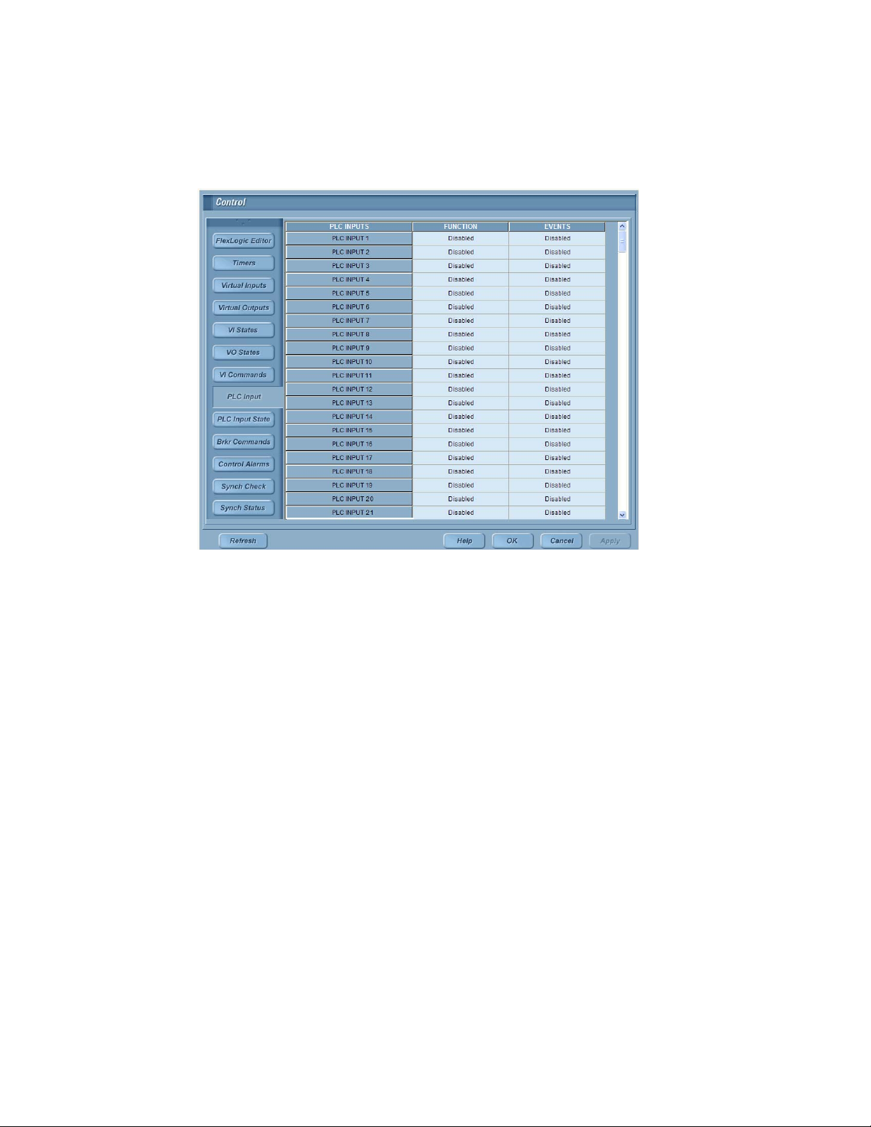
1.1.1.1 Configuration
User must set the parameters for each PLC Input from the PLC Input screen (Main Menu, User
Settings, Control).
Figure 1-1 PLC Input configuration screen
Function: Controls whether the input is either enabled or disabled. When input is disabled,
FlexLogic always reads its state as low. If input is enabled, FlexLogic reads the state from
corresponding Modbus register.
Events: When enabled, if there is transition of state, an event corresponding to the direction of
the transition will be logged.
Integrator’s Guide8
Page 9
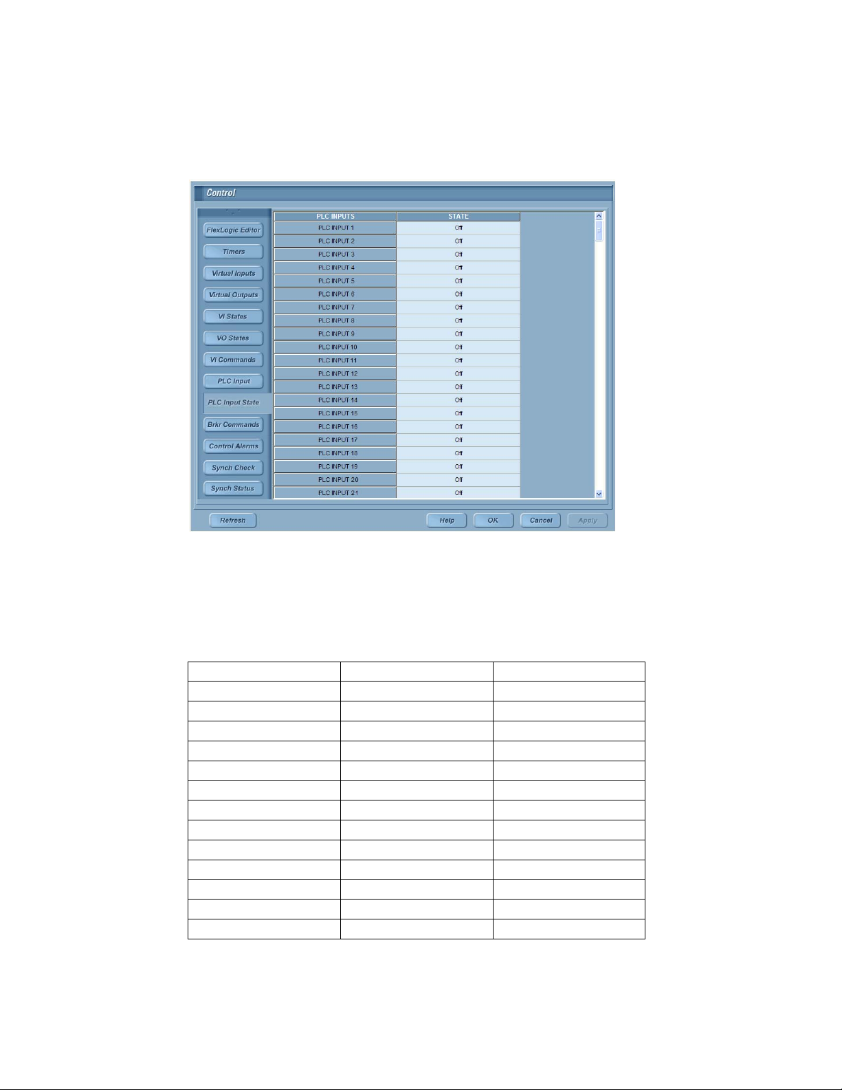
1.1.1.2 Status
To view a snapshot of the PLC input states from the HMI, open the PLC Input State screen (Main
Menu, User Settings, Control). Click refresh if update the status.
Figure 1-2 PLC Input States register format
1.1.1.3 PLC Input States
Each bit of the “PLC Input States” register represents one PLC input. Bit value 0 indicates the
corresponding PLC input is in off state; and bit value is 1 indicating corresponding PLC input is in
on state. See Table 1-1.
Table 1-1 PLC Input States register format
PLC Input States register PLC Input States bit field PLC Input X
101
2017
…
16 0 241
12
23
……
15 16
118
……
1242
……
15 256
PLC support 9
Page 10

1.1.2 FlexLogic Operand States
After each protection pass, all the information regarding each operand's state is updated in
corresponding Modbus register. The section PLC Interface (Read/Write) on page 110 is the
complete list of registers holding state information of corresponding operand.
1.1.2.1 Breaker Control Flex Operand States
Each breaker has 13 different states shown in Table 1-2. Each one of them corresponds to a
different bit in the data item.
Table 1-2 Breaker Control status bit field
Bit Value Notes
0 Breaker Opened
1Breaker Closed
2 Breaker Locked Out
3 Closing Spring Charged
4 Primary Disconnect Connected
5 Primary Disconnect Disconnected
6 Secondary Disconnect Connected
7Breaker Ready
8 Breaker Available
9 Breaker Open Failed
10 Breaker Close Failed
11 Breaker Fault
12 Breaker RELT State Not used in this release. It shall be always set to 0.
The breaker states for all 30 breakers span across 25 consecutive modbus registers as shown in
Table 1-3. See PLC Interface (Read/Write) on page 110 for memory locations.
Table 1-3 Breaker status offsets
Breaker Number Register
Offset
Breaker 1 0 0 N/A
Breaker 2 0 13 This breaker’s information spans
Breaker 3 1 10 This breaker’s information spans
Bit Offset Notes
over two adjacent registers
over two adjacent registers
Breaker 4 2 7 This breaker’s information spans
over two adjacent registers
... ... ... ...
Integrator’s Guide10
Page 11
1.1.2.2 Bus Differential Flex Operand States
Each zone has 6 different states shown in Table 1-4. Each one of them corresponds to a different bit
in the data item.
Table 1-4 Bus Differential status bit field
Bit Value
0 Trip Dropout
1 Alarm Dropout
2 Trip Pickup
3Alarm Pickup
4 Trip Operated
5 Alarm Operated
6 Backup Trip Operated
The zone states for all 4 relay instances span across 2 consecutive modbus registers as shown in
Table 1-3. See PLC Interface (Read/Write) on page 110 for memory locations.
Table 1-5 Bus Differential status offsets
Zone Number Register
Offset
Bit Offset Notes
Zone 1 0 0
Zone 2 0 7
Zone 3 0 14 This zone’s information spans
over two adjacent registers
Zone 4 1 5
1 12 Bits from 12 thru 15 are not used
and shall always be set to 0
PLC support 11
Page 12

1.1.2.3 Ground Fault Flex Operand States
Each breaker has 5 different states shown in Table 1-6. Each one of them corresponds to a different
bit in the data item.
Table 1-6 Ground Fault status bit field
Bit Value
0 Trip Pickup
1 Trip Operated
2 Trip Dropout
3Alarm Pickup
4 Alarm Operated
5 Alarm Dropout
The breaker states for all 30 breakers span across 12 consecutive modbus registers as shown in
Table 1-7. See PLC Interface (Read/Write) on page 110 for memory locations.
Table 1-7 Ground Fault status offsets
Breaker Number Register
Offset
Bit Offset Notes
Breaker 1 0 0
Breaker 2 0 6
Breaker 3 0 12 This breaker’s information spans
over two adjacent registers
Breaker 4 1 2
... ... ... ...
Integrator’s Guide12
Page 13

1.1.2.4 High Current and High Current Transient Flex Operand States
Each breaker has 3 different states shown in Table 1-8. Each one of them corresponds to a different
bit in the data item.
Table 1-8 High Current status bit field
Bit Value
0Alarm Pickup
1 Alarm Operated
2 Alarm Dropout
The breaker states for all 30 breakers span across 6 consecutive modbus registers as shown in
Table 1-9. See PLC Interface (Read/Write) on page 110 for memory locations.
Table 1-9 High Current status offsets
Breaker Number Register
Offset
Breaker 1 0 0
Breaker 2 0 3
Breaker 3 0 6
Bit Offset Notes
Breaker 4 0 9
... ... ... ...
PLC support 13
Page 14

1.1.2.5 HRGF Detection Flex Operand States
Each breaker has 3 different states shown in Table 1-10. Each one of them corresponds to a
different bit in the data item.
Table 1-10 HRGF Detection status bit field
Bit Value
0 Alarm Dropout
1Alarm Pickup
2 Alarm Operated
The breaker states for all 30 breakers span across 6 consecutive modbus registers as shown in
Table 1-11. See PLC Interface (Read/Write) on page 110 for memory locations.
Table 1-11 HRGF Detection status offsets
Breaker Number Register
Offset
Breaker 1 0 0
Breaker 2 0 3
Breaker 3 0 6
Bit Offset Notes
Breaker 4 0 9
... ... ... ...
Integrator’s Guide14
Page 15

1.1.2.6 HRGF Location Flex Operand States
Each zone has 2 different states shown in Table 1-12. Each one of them corresponds to a different
bit in the data item.
Table 1-12 HRGF Location status bit field
Bit Value
0 Locator in On State
1 Locator in Off State
The zone states for all 4 location function instances are contained in a single modbus register as
shown in
Table 1-13 HRGF Location status offsets
Zone Number Register
Zone 1 0 0
Zone 2 0 2
Zone 3 0 4
Zone 4 0 6
Table 1-13. See PLC Interface (Read/Write) on page 110 for memory locations.
Offset
Bit Offset Notes
0 8 Bits from 8 thru 15 are not used
and shall always be set to 0
PLC support 15
Page 16

1.1.2.7 IOC Flex Operand States
Each breaker has 2 different states shown in Table 1-14. Each one of them corresponds to a
different bit in the data item.
Table 1-14 IOC status bit field
Bit Value
0 Trip Operated
1 Trip Dropout
The breaker states for all 30 breakers span across 4 consecutive modbus registers as shown in
Table 1-15. See PLC Interface (Read/Write) on page 110 for memory locations.
Table 1-15 IOC status offsets
Breaker Number Register
Breaker 1 0 0
Breaker 2 0 2
Breaker 3 0 4
Breaker 4 0 6
Bit Offset Notes
Offset
Breaker 5 0 8
Breaker 6 0 10
Breaker 7 0 12
Breaker 8 0 14
Breaker 9 1 0
... ... ...
Integrator’s Guide16
Page 17

1.1.2.8 LT Overcurrent Flex Operand States
Each breaker has 3 different states shown in Table 1-16. Each one of them corresponds to a
different bit in the data item.
Table 1-16 LT Overcurrent status bit field
Bit Value
0Alarm Pickup
1 Alarm Operated
2 Alarm Dropout
The breaker states for all 30 breakers span across 6 consecutive modbus registers as shown in
Table 1-17. See PLC Interface (Read/Write) on page 110 for memory locations.
Table 1-17 LT Overcurrent status offsets
Breaker Number Register
Offset
Breaker 1 0 0
Breaker 2 0 3
Breaker 3 0 6
Breaker 4 0 9
Breaker 5 0 12
Breaker 6 0 15 This breaker’s information spans
... ... ...
Bit Offset Notes
over two adjacent registers
PLC support 17
Page 18

1.1.2.9 MSGF Overcurrent Flex Operand States
Each zone has 7 different states shown in Table 1-18. Each one of them corresponds to a different
bit in the data item.
Table 1-18 MSGF Overcurrent status bit field
Bit Value
0 Trip Dropout
1 Alarm Dropout
2 Trip Pickup
3Alarm Pickup
4 Trip Operated
5 Alarm Operated
6 Backup Trip Operated
The zone states for all 4 instances span across 2 consecutive modbus registers as shown in
Table 1-19. See PLC Interface (Read/Write) on page 110 for memory locations.
Table 1-19 MSGF Overcurrent status offsets
Zone Number Register
Offset
Zone 1 0 0
Zone 2 0 7
Zone 3 0 14 This zone’s information spans
Zone 4 1 5
1 12 Bits from 12 thru 15 are not used
Bit Offset Notes
over two adjacent registers
and shall always be set to 0
Integrator’s Guide18
Page 19

1.1.2.10 Multi Point RELT Flex Operand States
This relay has 1 state shown in Table 1-20.
Table 1-20 Multi Point RELT status bit field
Bit Value
0 Multipoint Reduced Let-Thru Mode On
The relay state uses one modbus register as shown in Table 1-21. See PLC Interface (Read/Write)
on page 110 for memory locations.
Table 1-21 Multi Point RELT status offsets
Zone Number Register
Offset
RELT State 0 0
0 1 Bits from 1 thru 15 are not used
Bit Offset Notes
and shall always be set to 0
PLC support 19
Page 20

1.1.2.11 Over (and Under) Frequency Flex Operand States
Each breaker has 6 different states shown in Table 1-22. Each one of them corresponds to a
different bit in the data item.
Table 1-22 Over Frequency status bit field
Bit Value
0Alarm Pickup
1 Alarm Operated
2 Alarm Dropout
3 Trip Pickup
4 Trip Operated
5 Trip Dropout
The breaker states for all 30 breakers span across 12 consecutive modbus registers as shown in
Table 1-23. See PLC Interface (Read/Write) on page 110 for memory locations.
Table 1-23 Over Frequency status offsets
Breaker Number Register
Offset
Breaker 1 0 0
Breaker 2 0 6
Breaker 3 0 12 This breaker’s information spans
Breaker 4 1 2
... ... ...
Bit Offset Notes
over two adjacent registers
Integrator’s Guide20
Page 21

1.1.2.12 Over (and Under) Voltage Flex Operand States
Each breaker has 6 different states shown in Table 1-24. Each one of them corresponds to a
different bit in the data item.
Table 1-24 Over Voltage status bit field
Bit Value
0Alarm Pickup
1 Alarm Operated
2 Alarm Dropout
3 Trip Pickup
4 Trip Operated
5 Trip Dropout
The breaker states for all 30 breakers span across 12 consecutive modbus registers as shown in
Table 1-25. See PLC Interface (Read/Write) on page 110 for memory locations.
Table 1-25 Over Voltage status offsets
Breaker Number Register
Offset
Breaker 1 0 0
Breaker 2 0 6
Breaker 3 0 12 This breaker’s information spans
Breaker 4 1 2
... ... ...
Bit Offset Notes
over two adjacent registers
PLC support 21
Page 22

1.1.2.13 Phase Loss Flex Operand States
Each breaker has 6 different states shown in Table 1-26. Each one of them corresponds to a
different bit in the data item.
Table 1-26 Phase Loss status bit field
Bit Value
0Alarm Pickup
1 Alarm Operated
2 Alarm Dropout
3 Trip Pickup
4 Trip Operated
5 Trip Dropout
The breaker states for all 30 breakers span across 12 consecutive modbus registers as shown in
Table 1-27. See PLC Interface (Read/Write) on page 110 for memory locations.
Table 1-27 Phase Loss status offsets
Breaker Number Register
Offset
Breaker 1 0 0
Breaker 2 0 6
Breaker 3 0 12 This breaker’s information spans
Breaker 4 1 2
... ... ...
Bit Offset Notes
over two adjacent registers
Integrator’s Guide22
Page 23

1.1.2.14 Power Reversal Flex Operand States
Each breaker has 6 different states shown in Table 1-28. Each one of them corresponds to a
different bit in the data item.
Table 1-28 Power Reversal status bit field
Bit Value
0Alarm Pickup
1 Alarm Operated
2 Alarm Dropout
3 Trip Pickup
4 Trip Operated
5 Trip Dropout
The breaker states for all 30 breakers span across 12 consecutive modbus registers as shown in
Table 1-29. See PLC Interface (Read/Write) on page 110 for memory locations.
Table 1-29 Power Reversal status offsets
Breaker Number Register
Offset
Breaker 1 0 0
Breaker 2 0 6
Breaker 3 0 12 This breaker’s information spans
Breaker 4 1 2
... ... ...
Bit Offset Notes
over two adjacent registers
PLC support 23
Page 24

1.1.2.15 ST Overcurrent Flex Operand States
Each breaker has 3 different states shown in Table 1-30. Each one of them corresponds to a
different bit in the data item.
Table 1-30 ST Overcurrent status bit field
Bit Value
0 Trip Pickup
1 Trip Operated
2 Trip Dropout
The breaker states for all 30 breakers span across 6 consecutive modbus registers as shown in
Table 1-31. See PLC Interface (Read/Write) on page 110 for memory locations.
Table 1-31 ST Overcurrent status offsets
Breaker Number Register
Offset
Breaker 1 0 0
Breaker 2 0 3
Breaker 3 0 6
Breaker 4 0 9
Breaker 5 0 12
Breaker 6 0 15 This breaker’s information spans
Breaker 7 1 2
... ... ...
Bit Offset Notes
over two adjacent registers
Integrator’s Guide24
Page 25

1.1.2.16 Summation MSGF Zone Flex Operand States
Each zone has 7 different states shown in Table 1-32. Each one of them corresponds to a different
bit in the data item.
Table 1-32 Summation MSGF Zone status bit field
Bit Value
0 Trip Dropout
1 Alarm Dropout
2 Trip Pickup
3Alarm Pickup
4 Trip Operated
5 Alarm Operated
6 Trip Restrained
The zone states for both zones reside in a single modbus register as shown in Table 1-33. See PLC
Interface (Read/Write) on page 110 for memory locations.
Table 1-33 Summation MSGF Zone status offsets
Zone Number Register
Offset
Zone 1 0 0
Zone 2 0 8
Bit Offset Notes
PLC support 25
Page 26

1.1.2.17 Synch Check Flex Operand States
Each relay has 10 different states shown in Table 1-34. Each one of them corresponds to a different
bit in the data item.
Table 1-34 Synch Check status bit field
Bit Value
0 Dead Source Operated
1 Dead Source Dropout
2 Synch Operated
3 Synch Dropout
4 Close Operated
5 Close Dropout
6V1 Above Minimum
7V2 Above Minimum
8 V1 Below Maximum
9 V2 Below Maximum
The relay states for all12 relays span across 8 consecutive modbus registers as shown in Table 1-35.
See
PLC Interface (Read/Write) on page 110 for memory locations.
Table 1-35 Synch Check status offsets
Zone Number Register
Offset
Relay 1 0 0
Relay 2 0 10 This relay’s information spans
Relay 3 1 4
Relay 4 1 14 This relay’s information spans
Relay 5 2 8 This relay’s information spans
Relay 6 3 2
Relay 7 3 12
Relay 8 4 6
Relay 9 5 0
Relay 10 5 10
Bit Offset Notes
over two adjacent registers
over two adjacent registers
over two adjacent registers
Relay 11 6 4
Relay 12 6 14
7 8 Bits from 8 thru 15 are not used
and shall always be set to 0
Integrator’s Guide26
Page 27

2 Modbus® protocol implementation
2.1 Introduction
The CPU supports a number of communications protocols to allow connection to the HMI
computer, as well as other equipment which includes personal computers, RTUs, SCADA
masters, and programmable logic controllers. The Modicon Modbus® RTU protocol is the most
basic protocol supported. Modbus is available via ethernet as specified by the Modbus/TCP
specification. Note that:
• The CPU always acts as a slave device, meaning that it never initiates communications; it
only listens and responds to requests issued by a master computer.
• For Modbus, a subset of the Remote Terminal Unit (RTU) protocol format is supported that
allows extensive monitoring, programming, and control functions using read and write
register commands.
• The CPU will support a maximum of 8 concurrent Modbus sessions. Four sessions are
reserved for use by HMI computers. A remote device that attempts to connect when all
sessions are in use will receive a response message indicating the number of maximum
connections has been exceeded. If a remote device does not make a request within
30 seconds, the session will be timed out and made available to the next device that
establishes a session.
2
2.2 Physical layer
The Modbus RTU protocol is hardware-independent so that the physical layer can be any of a
variety of standard hardware configurations. The CPU includes a faceplate (front panel)
100BaseT Ethernet port. Data flow is auto-configuring full or half-duplex. Each data byte is
transmitted in an asynchronous format consisting of 1 start bit, 8 data bits, 1 stop bit , and
possibly 1 parity bit. This produces a 10 or 11 bit data frame. The master device in any system
must know the address of the slave device with which it is to communicate. In the case of
ModbusTCP communications, the CPU will not act on a request from a master if the address in
the request does not match the CPU’s slave address. A single setting selects the slave address
used for ModbusTCP. The default slave address for a CPU is 1.
Introduction 27
Page 28

2.3 Data link layer
22
Communications takes place in packets, which are groups of asynchronously framed byte data.
The master transmits a packet to the slave and the slave responds with a packet. The end of a
packet is marked by ‘dead-time’ on the communications line. The following describes general
format for both transmit and receive packets. For exact details on packet formatting, see the
subsequent sections describing each function code.
MODBUS PACKET FORMAT
DESCRIPTION SIZE
SLAVE ADDRESS 1 byte
FUNCTION CODE 1 byte
DATA N bytes
CRC 2 bytes
DEAD TIME 3.5 bytes transmission time
SLAVE ADDRESS
This is the address of the slave device that is intended to receive the packet sent by the master
and perform the desired action. Only the addressed slave will respond to a packet that starts
with its address. Note that since Modbus/TCP also relies on a correct IP address to receive the
packet, and each CPU responds as a single device, it is generally not necessary to change the
Modbus address of the device.
FUNCTION CODE
This is one of the supported function codes of the unit which tells the slave what action to
perform. See Supported function codes
from the slave is indicated by setting the high order bit of the function code in the response
packet. See Exception responses on page 35 for further details.
DATA
This will be a variable number of bytes depending on the function code. This may include actual
values, settings, or addresses sent by the master to the slave or by the slave to the master.
CRC
This is a two byte error checking code. The RTU version of Modbus includes a 16-bit cyclic
redundancy check (CRC-16) with every packet which is an industry standard method used for
error detection. If a Modbus slave device receives a packet in which an error is indicated by the
CRC, the slave device will not act upon or respond to the packet thus preventing any erroneous
operations. See CRC-16 Algorithm
on page 30 for complete details. An exception response
on page 29 for a description of how to calculate the CRC.
Modbus® protocol implementation28
Page 29

2.4 CRC-16 Algorithm
The CRC-16 algorithm essentially treats the entire data stream (data bits only; start, stop and
parity ignored) as one continuous binary number. This number is first shifted left 16 bits and
then divided by a characteristic polynomial (11000000000000101B). The 16-bit remainder of the
division is appended to the end of the packet, most significant byte first. The resulting packet
including CRC, when divided by the same polynomial at the receiver, will give a zero remainder if
no transmission errors have occurred. This algorithm requires the characteristic polynomial to
be reverse bit ordered. The most significant bit of the characteristic polynomial is dropped, since
it does not affect the value of the remainder.
CRC-16 ALGORITHM
SYMBOLS --> data transfer
A 16-bit working register
Alow low order byte of A
Ahigh high order byte of A
CRC 16-bit CRC-16 result
i,j loop counters
(+) logical EXCLUSIVE-OR operator
2
N total number of data bytes
Di i-th data byte (i = 0 to N-1)
G 16-bit characteristic polynomial = 1010000000000001 (binary) with
MSbit dropped and bit order reversed
shr (x) right shift operator (th LSbit of x is shifted into a carry flag, a ‘0’ is
shifted into the MSbit of x, all other bits are shifted right one location)
ALGORITHM:
1. FFFF (hex) --> A
2. 0 --> i
3. 0 --> j
4. Di (+) Alow --> Alow
5. j + 1 --> j
6. shr (A)
7. Is there a carry? No: go to 8 Yes: G (+) A --> A and continue.
8. Is j = 8? No: go to 5 Yes: continue
9. i + 1 --> i
10. Is i = N? No: go to 3 Yes: continue
11. A --> CRC
CRC-16 Algorithm 29
Page 30

2
2.5 Supported function codes
Modbus officially defines function codes from 1 to 127 though only a small subset is generally
needed. The CPU supports some of these functions, as summarized in the following table.
Subsequent sections describe each function code in detail.
2.5.1 Function Code 03H/04H – Read Actual Values or Settings
This function code allows the master to read one or more consecutive data registers (actual
values or settings) from a relay. Data registers are always 16 bit (two byte) values transmitted
with high order byte first . The maximum number of registers that can be read in a single packet
is 125. See the MODBUS MEMORY MAP table on page 17 for exact details on the data registers.
Since some PLC implementations of Modbus only support one of function codes 03h and 04h,
the CPU interpretation allows either function code to be used for reading one or more
consecutive data registers. The data starting address will determine the type of data being read.
Function codes 03h and 04h are therefore identical. The following table shows the format of the
master and slave packets. The example shows a master device requesting 3 register values
starting at address 4050h from slave device 11h (17 decimal); the slave device responds with
the values 40, 300, and 0 from registers 4050h, 4051h, and 4052h, respectively.
FUNCTION CODE MODBUS DEFINITION CPU DEFINITION
HEX DEC
03 3 Read Holding Registers Read Actual Values or Settings
04 4 Read Holding Registers Read Actual Values or Settings
05 5 Force Single Coil Execute Operation
06 6 Preset Single Register Store Single Setting
10 16 Preset Multiple Registers Store Multiple Settings
Modbus® protocol implementation30
Page 31

Master and Slave Device Packet Transmission Example
MASTER TRANSMISSION
PACKET FORMAT EXAMPLE (HEX)
SLAVE ADDRESS 11
FUNCTION CODE 04
DATA STARTING ADDR - hi 40
DATA STARTING ADDR - lo 50
NUMBER OF REGISTERS - hi 00
NUMBER OF REGISTERS - lo 03
CRC - lo A7 DATA #2 - lo A7
CRC - hi 4A DATA #3 - hi 4A
SLAVE RESPONSE
PACKET FORMAT EXAMPLE (HEX)
2
SLAVE ADDRESS 11
FUNCTION CODE 04
BYTE COUNT 06
DATA #1 - hi 00
DATA #1 - lo 28
DATA #2 - hi 01
DATA #2 - lo 2C
DATA #3 - hi 00
DATA #3 - lo 00
CRC - lo 0D
CRC - hi 60
Supported function codes 31
Page 32

2
2.5.2 Function Code 05H – Execute Operation
This function code allows the master to perform various operations in the CPU.
The following table shows the format of the master and slave packets. The example shows a
master device requesting the slave device 11H (17 dec) to perform a reset. The hi and lo CODE
VALUE bytes always have the values ‘FF’ and ‘00’ respectively and are a remnant of the original
Modbus definition of this function code.
Master and Slave Device Packet Transmission Example
MASTER TRANSMISSION
PACKET FORMAT EXAMPLE (HEX)
SLAVE ADDRESS 11
FUNCTION CODE 05
OPERATION CODE - hi 00
OPERATION CODE - lo 01
CODE VALUE - hi FF
CODE VALUE - lo 00
CRC - lo DF
CRC - hi 6A
SLAVE RESPONSE
PACKET FORMAT EXAMPLE (HEX)
SLAVE ADDRESS 11
FUNCTION CODE 05
OPERATION CODE - hi 00
OPERATION CODE - lo 01
CODE VALUE - hi FF
CODE VALUE - lo 00
CRC - lo DF
CRC - hi 6A
Modbus® protocol implementation32
Page 33

2.5.3 Function Code 06H – Store Single Setting
This function code allows the master to modify the contents of a single setting register in a CPU.
Setting registers are always 16-bit (two byte) values transmitted high-order byte first. The
following table shows the format of the master and slave packets. The example shows a master
device storing the value 200 at memory map address 4051h to slave device 11h (17 dec).
Master and Slave Device Packet Transmission Example
MASTER TRANSMISSION
PACKET FORMAT EXAMPLE (HEX)
SLAVE ADDRESS 11
FUNCTION CODE 06
DATA STARTING ADDR - hi 40
DATA STARTING ADDR - lo 51
DATA - hi 00
DATA - lo C8
2
CRC - lo CE
CRC - hi DD
SLAVE RESPONSE
PACKET FORMAT EXAMPLE (HEX)
SLAVE ADDRESS 11
FUNCTION CODE 06
DATA STARTING ADDR - hi 40
DATA STARTING ADDR - lo 51
DATA - hi 00
DATA - lo C8
CRC - lo CE
CRC - hi DD
Supported function codes 33
Page 34

2
2.5.4 Function Code 10H – Store Multiple Settings
This function code allows the master to modify the contents of a one or more consecutive
setting registers in a CPU. Setting registers are 16-bit (two byte) values transmitted high-order
byte first. The maximum number of setting registers that can be stored in a single packet is 60.
The following table shows the format of the master and slave packets. The example shows a
master device storing the value 200 at memory map address 4051h, and the value 1 at memory
map address 4052h to slave device 11h (17 dec).
Master and Slave Device Packet Transmission Example
MASTER TRANSMISSION
PACKET FORMAT EXAMPLE (HEX)
SLAVE ADDRESS 11
FUNCTION CODE 10
DATA STARTING ADDR-hi 40
DATA STARTING ADDR-lo 51
NUMBER OF SETTINGS-hi 00
NUMBER OF SETTINGS-lo 02
BYTE COUNT 04
DATA #1 - hi 00
DATA #1 - lo C8
DATA #2 - hi 00
DATA #2 - lo 01
CRC – lo 12
CRC – hi 62
Modbus® protocol implementation34
Page 35

SLAVE RESPONSE
PACKET FORMAT EXAMPLE (HEX)
SLAVE ADDRESS 11
FUNCTION CODE 10
DATA STARTING ADDR - hi 40
DATA STARTING ADDR - lo 51
NUMBER OF SETTINGS - hi 00
NUMBER OF SETTINGS - lo 02
CRC - lo 07
CRC - hi 64
2.5.5 Exception responses
Programming or operation errors usually happen because of illegal data in a packet. These
errors result in an exception response from the slave. The slave detecting one of these errors
sends a response packet to the master with the high order bit of the function code set to 1. The
following table shows the format of the master and slave packets. The example shows a master
device sending the unsupported function code 39h to slave device 11.
2
Master and Slave Device Packet Transmission Example
MASTER TRANSMISSION
PACKET FORMAT EXAMPLE (HEX)
SLAVE ADDRESS 11
FUNCTION CODE 39
CRC - low order byte CD
CRC - high order byte F2
SLAVE RESPONSE
PACKET FORMAT EXAMPLE (HEX)
SLAVE ADDRESS 11
FUNCTION CODE B9
ERROR CODE 01
Supported function codes 35
Page 36

2
SLAVE RESPONSE
CRC - low order byte 93
CRC - high order byte 95
2.5.6 File transfers
2.5.6.1 Obtaining CPU files using Modbus protocol
The CPU has a generic file transfer facility, meaning that you use the same method to obtain all
of the different types of files from the unit. The Modbus registers that implement file transfer are
found in the “Modbus File Transfer (Read/Write)” and “Modbus File Transfer (Read Only)”
modules, starting at address 030Eh in the Modbus Memory Map. To read a file from the CPU, use
the following steps:
1. Write the filename to the “Name of file to read” register using a write multiple registers
command. If the name is shorter than 80 characters, you may write only enough registers to
include all the text of the filename. Filenames are not case sensitive.
2. Repeatedly read all the registers in “Modbus File Transfer (Read Only)” using a read multiple
registers command. It is not necessary to read the entire data block, since the CPU will
remember which was the last register read. The “position” register is initially zero and
thereafter indicates how many bytes (2 times the number of registers) you have read so far.
The “size of...” register indicates the number of bytes of data remaining to read, to a
maximum of 244.
3. Keep reading until the “size of...” register is smaller than the number of bytes you are
transferring. This condition indicates end of file. Discard any bytes you have read beyond the
indicated block size.
4. If you need to re-try a block, read only the “size of...” and “block of data”, without reading the
position. The file pointer is only incremented when you read the position register, so the
same data block will be returned as was read in the previous operation. On the next read,
check to see if the position is where you expect it to be, and discard the previous block if it is
not (this condition would indicate that the CPU did not process your original read request).
The CPU retains connection-specific file transfer information, so files may be read
simultaneously on multiple Modbus connections.
a. Obtaining files from the CPU using other protocols
All the files available via Modbus may also be retrieved using the standard file transfer
mechanisms in other protocols (for example, TFTP).
b. Reading event recorder files
To read the entire event recorder contents in ASCII format (the only available format), use
the following filename:
•EVT.TXT
c. Reading fault report files
The file name for fault report data is faultReport#####.txt. The ##### refers to the
fault report record number. This number is identical to the event record number
associated with the fault report . A request for a non-existent fault report file will yield file
with no data below the header.
Modbus® protocol implementation36
Page 37

d. Reading waveform capture files
Waveform records comply with COMTRADE 1999 format (IEEE Std C37.111-1999). The file
names as required by the standard for waveform capture data are wfc#####.dat and
wfc#####.cfg. The ##### refers to the waveform record number. Note that this number
is not the same as the event number cited in the case of the fault report above. If an
event has a waveform capture associated with it, the waveform number will be shown in
the WF Number field as indicated in the header of the event log.
2.5.7 Modbus password operation
The COMMAND password is set up at memory location 0458h. Storing a value of “0” removes
COMMAND password protection. When reading the password setting, the encrypted value (zero
if no password is set) is returned. COMMAND security is required to change the COMMAND
password.
Similarly, the SETTING password is set up at memory location 045Ah. To gain COMMAND level
security access, the COMMAND password must be entered at memory location 045Ch. To gain
SETTING level security access, the SETTING password must be entered at memory location
045Eh. The entered SETTING password must match the current SETTING password setting, or
must be zero, to change settings or download firmware.
COMMAND and SETTING passwords each have a 30-minute timer. Each timer starts when you
enter the particular password, and is restarted whenever you “use” it. For example, writing a
setting restarts the SETTING password timer and writing a command register or forcing a coil
restarts the COMMAND password timer. The value read at memory location 0460h can be used
to confirm whether a COMMAND password is enabled or disabled (0 for Disabled). The value
read at memory location 0461h can be used to confirm whether a SETTING password is enabled
or disabled.
2
COMMAND or SETTING password security access is restricted to the particular port or particular
TCP/IP connection on which the entry was made. Passwords must be entered when accessing
the relay through other ports or connections, and the passwords must be reentered after
disconnecting and reconnecting on TCP/IP.
Supported function codes 37
Page 38

2
2.6 Interfacing to the Alarm Handler
The set of registers beginning at 0648h provides the means to interface to each CPU’s Alarm
Handler functionality. Each pair of 32-bit values represent the current state (read only) and the
acknowledge setting (read/write) for each alarm type. Each value represents the states for all of
the circuit breakers in the system as denoted in Format Code F722, one bit for each. A 1 in the
bit field position for a given circuit breaker in the state register indicates that the alarm
condition is currently active, while a 0 indicates the condition is not currently active.
When a condition passes from inactive to active, the corresponding ACK bit in the next register
will be set to 1. At this point an external program may acknowledge the alarm by writing a 0 to
that bit location. It is important for the external program to first read the ACK register and mask
the new value such that the states represented by the other bits remain intact. The following
state table describes how the HMI interfaces with the CPU to update its indicators.
Figure 2-3 Alarm state transition diagram
Start
System Initialization
ACK: 0
Status: 0
HMI Color:
Green
HMI
ACK
Alarm Condition
Condition
Goes Normal
Occurs
HMI
ACK
ACK: 0
Status: 1
HMI Color:
Solid
Red
ACK: 1
Status: 0
HMI Color:
Yellow
ACK: 1
Status: 1
HMI Color:
Blinking
Red
Condition
Goes Normal
Condition
Recurs
Alarm State Transition Diagram
Modbus® protocol implementation38
Page 39

3 Modbus Memory Map
NOTE: A multiplier factor may be necessary in cases where an integer value is returned but the
Range and/or Step imply a greater precision. In these cases, it is necessary to divide the
returned value by 10 for a step of “0.1” or “0.5”; by 100 for a step of “.01”; and so on. Similarly, it is
necessary to multiply by these factors prior to writing a settings value. This note does not apply
to any step value greater than 1 (a step of “10” does not require a multiplier, for example). This
note also does not apply to values returned in floating point format. See the format codes at the
end of the map for more information.
NOTE: Discrete I/O output state registers (Contact Output x State - register range from x9180
to x91FF and Contact Output States - register range from xB256 to 0xB25D) contain correct
information only when FlexLogic Active register (x0034) contains value 1 (yes).
Addr Register Name Range Units Step For-
mat
Product Information (Read Only)
0000 FBW Product Type 0 to 2 --- 1 F716 0 (Low Voltage
0001 Serial Number --- --- --- F203 “0”
Factory Default
Switchgear)
3
0009 External Ethernet MAC Address --- --- --- F072 0
000C Reserved (3 items) --- --- --- F001 0
000F CPU Hardware Version 0 to 655.35 --- 0.01 F001 100
0010 CPU Firmware Version 0 to 655.35 --- 0.01 F001 100
0011 CPU Firmware Boot Code Version 0 to 655.35 --- 0.01 F001 100
0012 Build Date --- --- --- F200 “0”
0026 Synchronizer Board Status 0 to 1 --- 1 F102 0 (Disabled)
0027 Synchronizer Board Frequency Setting 50 to 60 Hz 10 F001 60
0028 Last Energy Clear Date 0 to 4294967295 --- 1 F050 0
002A Last CPU Commissioned Date 0 to 4294967295 --- 1 F050 0
002C Expected Node Protocol Version 0 to 655.35 --- 0.01 F001 0
002D Summary Number --- --- --- F205 “0”
0033 Line Up 0 to 99 --- 1 F001 1
0034 System Frequency Detected 0 to 65535 Hz 1 F001 0
0035 CPU Modbus Map Version 0 to 655.35 --- 0.01 F001 450
39
Page 40

0036 Reserved --- --- --- F001 0
Installation (Read/Write Setting)
0080 CPU ID 0 to 1 --- 1 F717 0 (CCPU A)
3
0081 CPU Commissioned 0 to 1 --- 1 F102 0 (Disabled)
0082 CPU Name --- --- --- F200 “UNNAMED”
0096 System Frequency 50 to 60 Hz 10 F001 60
0097 Phase Rotation 0 to 1 --- 1 F106 0 (ABC)
Clock (Read/Write Setting)
00E0 RTC Set Time 0 to 4294967295 --- 1 F050 0
Clock (Read Only)
00E2 Date Time Changed 0 to 4294967295 --- 1 F050 0
Communications (Read/Write Setting)
00EC External Ethernet IP Address 0 to 4294967295 --- 1 F003 3232235876
00EE External Ethernet IP Subnet Mask 0 to 4294963200 --- 1 F003 4294967040
00F0 External Ethernet Gateway IP Address 0 to 4294967295 --- 1 F003 0
00F2 Reserved (5 items) --- --- --- F001 0
Event Recorder (Read Only)
0150 Events Since Last Clear 0 to 4294967295 --- 1 F003 0
0152 Number of Available Events 0 to 4294967295 --- 1 F003 0
0154 Event Recorder Last Cleared Date 0 to 4294967295 --- 1 F050 0
Modbus File Transfer (Read/Write)
0156 Name of file to read --- --- --- F204 (none)
Modbus File Transfer (Read Only)
017E Character position of current block within
file
0180 Size of currently-available data block 0 to 65535 --- 1 F001 0
0181 Block of data from requested file (122 items) 0 to 65535 --- 1 F001 0
Modbus File Transfer Area 2 (Read/Write)
01FB Name of file to read --- --- --- F204 (none)
Modbus File Transfer Area 2 (Read Only)
0223 Character position of current block within
file
0225 Size of currently-available data block 0 to 65535 --- 1 F001 0
0 to 4294967295 --- 1 F003 0
0 to 4294967295 --- 1 F003 0
Modbus Memory Map40
Page 41

0226 Block of data from requested file (122 items) 0 to 65535 --- 1 F001 0
Passwords (Read/Write)
02A0 Reserved (4 items) --- --- --- F001 0
02A4 Command Password Entry 0 to 4294967295 --- 1 F003 0
02A6 Setting Password Entry 0 to 4294967295 --- 1 F003 0
Passwords (Read Only)
02A8 Command Password Status 0 to 1 --- 1 F102 0 (Disabled)
02A9 Setting Password Status 0 to 1 --- 1 F102 0 (Disabled)
02AA Reserved (128 items) --- --- --- F001 0
Zone Manager (Read Only)
032A Current Topology State 0 to 255 --- 1 F001 0
032B Current Zone1 Topology 0 to 255 --- 1 F001 1
032C Current Zone2 Topology 0 to 255 --- 1 F001 1
032D Current Zone3 Topology 0 to 255 --- 1 F001 1
032E Current Zone4 Topology 0 to 255 --- 1 F001 1
3
032F Current Zone1 Topology PT Throwover 0 to 255 --- 1 F001 1
0330 Current Zone2 Topology PT Throwover 0 to 255 --- 1 F001 1
0331 Current Zone3 Topology PT Throwover 0 to 255 --- 1 F001 1
0332 Current Zone4 Topology PT Throwover 0 to 255 --- 1 F001 1
Zone Manager (Read/Write Command)
0333 Multipoint Relay Reduced Let Thru Enable 0 to 1 --- 1 F126 0 (No)
0334 Multipoint Relay Reduced Let Thru Reset 0 to 1 --- 1 F126 0 (No)
Zone Manager (Read Only)
0335 Multipoint Relay Reduced Let Thru State 0 to 1 --- 1 F108 0 (Off)
Zone Manager (Read/Write Setting)
0336 Multipoint Reduced Let Thru FlexLogic Trig-
ger
Zone Manager (Read Only)
0337 Multipoint Reduced Let Thru Enable Count 0 to 65535 --- 1 F001 0
0 to 65535 --- 1 F300 0
Event Recorder Commands (Read/Write Command)
0346 Event Recorder Clear Command 0 to 1 --- 1 F126 0 (No)
Energy Commands (Read/Write Command)
41
Page 42

3
0347 Energy Clear Command 0 to 1 --- 1 F126 0 (No)
Fault And Event Test Trigger (Read/Write Command)
0348 Fault Trigger Command 0 to 1 --- 1 F126 0 (No)
Demand (Read/Write Setting)
0349 Demand Subinterval Length 1 to 60 --- 1 F001 1
034A Demand Subintervals Per Interval 1 to 15 --- 1 F001 1
Demand (Read/Write Command)
034B Demand Reset All Command 0 to 1 --- 1 F126 0 (No)
Demand (Read Only)
034C Number Of Demand Resets All 0 to 4294963200 --- 1 F003 0
034E Last Demand Reset All DateTime 0 to 4294967295 --- 1 F050 0
Demand (Read/Write Command)
0350 Demand Log Clear All Command 0 to 1 --- 1 F126 0 (No)
Demand (Read Only)
0351 Demand Log Last Cleared All Date 0 to 4294967295 --- 1 F050 0
Waveform Capture (Read Only)
035D Number WF Records Available 0 to 65535 --- 1 F001 0
Waveform Capture (Read/Write Command)
035E Waveform Clear Command 0 to 1 --- 1 F126 0 (No)
Waveform Capture (Read Only)
035F Waveform Last Clear Date 0 to 4294967295 --- 1 F050 0
Waveform Capture (Read/Write Command)
0361 Waveform Trigger Command 0 to 1 --- 1 F126 0 (No)
Waveform Capture (Read/Write Setting)
0362 Waveform Trigger Mode 0 to 1 --- 1 F118 0 (Automatic
Overwrite)
0363 Waveform Trigger Position 0 to 119 Half
Cycles
Waveform Capture (Read Only)
1 F001 60
0364 Waveforms Since Last Clear 0 to 4294967295 --- 1 F003 0
0366 Reserved (2 items) --- --- --- F001 0
Waveform Capture (Read/Write Setting)
Modbus Memory Map42
Page 43

0368 Waveform Trigger Thru FlexLogic 0 to 65535 --- 1 F300 0
Preventive Maintenance (Read/Write Setting)
0370 Load Life Rating 800A 0 to 65535 --- 1 F001 2800
0371 Load Life Rating 1600A 0 to 65535 --- 1 F001 1200
0372 Load Life Rating 2000A 0 to 65535 --- 1 F001 1000
0373 Load Life Rating 3200A 0 to 65535 --- 1 F001 600
0374 Load Life Rating 4000A 0 to 65535 --- 1 F001 500
0375 Load Life Rating 5000A 0 to 65535 --- 1 F001 400
0376 Mechanical Life Rating 800A 0 to 65535 --- 1 F001 12500
0377 Mechanical Life Rating 1600A 0 to 65535 --- 1 F001 4000
0378 Mechanical Life Rating 2000A 0 to 65535 --- 1 F001 4000
0379 Mechanical Life Rating 3200A 0 to 65535 --- 1 F001 1500
037A Mechanical Life Rating 4000A 0 to 65535 --- 1 F001 1500
037B Mechanical Life Rating 5000A 0 to 65535 --- 1 F001 1500
037C Load Life Max Current 800A 1 to 50 --- 1 F001 15
3
037D Load Life Max Current 1600A 1 to 50 --- 1 F001 15
037E Load Life Max Current 2000A 1 to 50 --- 1 F001 15
037F Load Life Max Current 3200A 1 to 50 --- 1 F001 13
0380 Load Life Max Current 4000A 1 to 50 --- 1 F001 9
0381 Load Life Max Current 5000A 1 to 50 --- 1 F001 7
Hardware Information (Read Only)
03A0 Flash Lifetime 1 to 10 --- 1 F001 1
Source Vectors (Read/Write Setting)
0408 Reserved (2 items) --- --- --- F001 0
040A Expected Nodes X State 0 to 4294967295 --- 1 F722 0
040C Source Node Identifier LED X State 0 to 4294967295 --- 1 F722 0
040E Node Setting Changed X State 0 to 4294967295 --- 1 F722 0
Source Vectors (Read Only)
0410 Nodes Communicating X State 0 to 4294967295 --- 1 F722 0
0412 Nodes Commissioned X State 0 to 4294967295 --- 1 F722 0
0414 Duplicate Nodes X State 0 to 4294967295 --- 1 F722 0
0416 Node Internal Diagnostics X State 0 to 4294967295 --- 1 F722 0
0418 Node System Diagnostics X State 0 to 4294967295 --- 1 F722 0
43
Page 44

3
041A Node Hardware Diagnostics X State 0 to 4294967295 --- 1 F722 0
041C Node Reflected CPU Diagnostics X State 0 to 4294967295 --- 1 F722 0
041E Breaker Contact Position X State 0 to 4294967295 --- 1 F722 0
0420 Breaker Primary Connection X State 0 to 4294967295 --- 1 F722 0
0422 Breaker Lockout X State 0 to 4294967295 --- 1 F722 0
0424 Summations Suspended X State 0 to 4294967295 --- 1 F722 0
0426 Breaker Tripped X State 0 to 4294967295 --- 1 F722 0
Source Vectors (All Ack Vectors are Read/Write Setting; All State Vectors are Read Only)
0428 Undervoltage Trip Alarm State 0 to 4294967295 --- 1 F722 0
042A Undervoltage Trip Alarm Ack 0 to 4294967295 --- 1 F722 0
042C Undervoltage Alarm State 0 to 4294967295 --- 1 F722 0
042E Undervoltage Alarm Ack 0 to 4294967295 --- 1 F722 0
0430 Overvoltage Trip Alarm State 0 to 4294967295 --- 1 F722 0
0432 Overvoltage Trip Alarm Ack 0 to 4294967295 --- 1 F722 0
0434 Overvoltage Alarm State 0 to 4294967295 --- 1 F722 0
0436 Overvoltage Alarm Ack 0 to 4294967295 --- 1 F722 0
0438 Phase Loss Trip Alarm State 0 to 4294967295 --- 1 F722 0
043A Phase Loss Trip Alarm Ack 0 to 4294967295 --- 1 F722 0
043C Phase Loss Alarm State 0 to 4294967295 --- 1 F722 0
043E Phase Loss Alarm Ack 0 to 4294967295 --- 1 F722 0
0440 Reverse Power Trip Alarm State 0 to 4294967295 --- 1 F722 0
0442 Reverse Power Trip Alarm Ack 0 to 4294967295 --- 1 F722 0
0444 Reverse Power Alarm State 0 to 4294967295 --- 1 F722 0
0446 Reverse Power Alarm Ack 0 to 4294967295 --- 1 F722 0
0448 High Current Alarm State 0 to 4294967295 --- 1 F722 0
044A High Current Alarm Ack 0 to 4294967295 --- 1 F722 0
044C Underfrequency Trip Alarm State 0 to 4294967295 --- 1 F722 0
044E Underfrequency Trip Alarm Ack 0 to 4294967295 --- 1 F722 0
0450 Underfrequency Alarm State 0 to 4294967295 --- 1 F722 0
0452 Underfrequency Alarm Ack 0 to 4294967295 --- 1 F722 0
0454 Overfrequency Trip Alarm State 0 to 4294967295 --- 1 F722 0
0456 Overfrequency Trip Alarm Ack 0 to 4294967295 --- 1 F722 0
0458 Overfrequency Alarm State 0 to 4294967295 --- 1 F722 0
Modbus Memory Map44
Page 45

045A Overfrequency Alarm Ack 0 to 4294967295 --- 1 F722 0
045C High Resistance Ground Fault Alarm State 0 to 4294967295 --- 1 F722 0
045E High Resistance Ground Fault Alarm Ack 0 to 4294967295 --- 1 F722 0
0460 Breaker Open Failed Alarm State 0 to 4294967295 --- 1 F722 0
0462 Breaker Open Failed Alarm Ack 0 to 4294967295 --- 1 F722 0
0464 Long Time Overcurrent Trip Alarm State 0 to 4294967295 --- 1 F722 0
0466 Long Time Overcurrent Trip Alarm Ack 0 to 4294967295 --- 1 F722 0
0468 Short T ime Overcurrent Trip Alarm State 0 to 4294967295 --- 1 F722 0
046A Short Time Overcurrent Trip Alarm Ack 0 to 4294967295 --- 1 F722 0
046C Ground Fault Trip Alarm State 0 to 4294967295 --- 1 F722 0
046E Ground Fault Trip Alarm Ack 0 to 4294967295 --- 1 F722 0
0470 Ground Fault Alarm State 0 to 4294967295 --- 1 F722 0
0472 Ground Fault Alarm Ack 0 to 4294967295 --- 1 F722 0
0474 Analog IOC Trip Alarm State 0 to 4294967295 --- 1 F722 0
0476 Analog IOC Trip Alarm Ack 0 to 4294967295 --- 1 F722 0
3
0478 IOC Trip Alarm State 0 to 4294967295 --- 1 F722 0
047A IOC Trip Alarm Ack 0 to 4294967295 --- 1 F722 0
047C Node Control Power Lost State 0 to 4294967295 --- 1 F722 0
047E Node Control Power Lost Ack 0 to 4294967295 --- 1 F722 0
0480 Node Communication Lost State 0 to 4294967295 --- 1 F722 0
0482 Node Communication Lost Ack 0 to 4294967295 --- 1 F722 0
0484 Breaker Load Life 50 State 0 to 4294967295 --- 1 F722 0
0486 Breaker Load Life 50 Ack 0 to 4294967295 --- 1 F722 0
0488 Breaker Load Life 75 State 0 to 4294967295 --- 1 F722 0
048A Breaker Load Life 75 Ack 0 to 4294967295 --- 1 F722 0
048C Breaker Load Life 90 State 0 to 4294967295 --- 1 F722 0
048E Breaker Load Life 90 Ack 0 to 4294967295 --- 1 F722 0
0490 Breaker Accum Service Alarm State 0 to 4294967295 --- 1 F722 0
0492 Breaker Accum Service Alarm Ack 0 to 4294967295 --- 1 F722 0
0494 Breaker Mechanical Life 12 5 State 0 to 4294967295 --- 1 F722 0
0496 Breaker Mechanical Life 12 5 Ack 0 to 4294967295 --- 1 F722 0
0498 Breaker Mechanical Life 25 State 0 to 4294967295 --- 1 F722 0
049A Breaker Mechanical Life 25 Ack 0 to 4294967295 --- 1 F722 0
45
Page 46

3
049C Breaker Mechanical Life 37 5 State 0 to 4294967295 --- 1 F722 0
049E Breaker Mechanical Life 37 5 Ack 0 to 4294967295 --- 1 F722 0
04A0 Breaker Mechanical Life 50 State 0 to 4294967295 --- 1 F722 0
04A2 Breaker Mechanical Life 50 Ack 0 to 4294967295 --- 1 F722 0
04A4 Breaker Mechanical Life 62 5 State 0 to 4294967295 --- 1 F722 0
04A6 Breaker Mechanical Life 62 5 Ack 0 to 4294967295 --- 1 F722 0
04A8 Breaker Mechanical Life 75 State 0 to 4294967295 --- 1 F722 0
04AA Breaker Mechanical Life 75 Ack 0 to 4294967295 --- 1 F722 0
04AC Breaker Mechanical Life 87 5 State 0 to 4294967295 --- 1 F722 0
04AE Breaker Mechanical Life 87 5 Ack 0 to 4294967295 --- 1 F722 0
04B0 Breaker Mechanical Life 100 State 0 to 4294967295 --- 1 F722 0
04B2 Breaker Mechanical Life 100 Ack 0 to 4294967295 --- 1 F722 0
04B4 Bus Differential Trip Alarm State 0 to 4294967295 --- 1 F722 0
04B6 Bus Differential Trip Alarm Ack 0 to 4294967295 --- 1 F722 0
04B8 Bus Differential Alarm State 0 to 4294967295 --- 1 F722 0
04BA Bus Differential Alarm Ack 0 to 4294967295 --- 1 F722 0
04BC Multi Source Ground Fault Trip Alarm State 0 to 4294967295 --- 1 F722 0
04BE Multi Source Ground Fault Trip Alarm Ack 0 to 4294967295 --- 1 F722 0
04C0 Multi Source Ground Fault Alarm State 0 to 4294967295 --- 1 F722 0
04C2 Multi Source Ground Fault Alarm Ack 0 to 4294967295 --- 1 F722 0
04C4 Hardware Synch Card Lost State 0 to 4294967295 --- 1 F722 0
04C6 Hardware Synch Card Lost Ack 0 to 4294967295 --- 1 F722 0
04CA Compartment ID Button Missing Alarm State 0 to 4294967295 --- 1 F722 0
04CE Compartment ID Button Missing Alarm Ack 0 to 4294967295 --- 1 F722 0
04D0 Control Alarm State 0 to 4294967295 --- 1 F722 0
04D2 Control Alarm Ack 0 to 4294967295 --- 1 F722 0
04D4 Redundant CPU Node Comm Loss State 0 to 4294967295 --- 1 F722 0
04D6 Redundant CPU Node Comm Loss Ack 0 to 4294967295 --- 1 F722 0
04D8 Redundant CPU Hardware Synch Loss State 0 to 4294967295 --- 1 F722 0
04DA Redundant CPU Hardware Synch Loss Ack 0 to 4294967295 --- 1 F722 0
04DC Discrete IO Misconfigured State 0 to 4294967295 --- 1 F722 0
04DE Discrete IO Misconfigured Ack 0 to 4294967295 --- 1 F722 0
04E0 Reserved (8 items) --- --- --- F001 0
Modbus Memory Map46
Page 47

04E8 HRGF Location Alarm State 0 to 4294967295 --- 1 F722 0
04EA HRGF Location Alarm Ack 0 to 4294967295 --- 1 F722 0
04EC Reserved (28 items) --- --- --- F001 0
0508 SRC X Node Ground CT Connected 0 to 4294967295 --- 1 F722 0
050A High Current Trigger Alarm State 0 to 4294967295 --- 1 F722 0
050C High Current Trigger Alarm Ack 0 to 4294967295 --- 1 F722 0
050E Reduced Let Thru Over 8 Hours Alarm State 0 to 4294967295 --- 1 F722 0
0510 Reduced Let Thru Over 8 Hours Alarm Ack 0 to 4294967295 --- 1 F722 0
3
0512 HRGF Location Contactor Operating Alarm
State
0514 HRGF Location Contactor Operating Alarm
Ack
0516 HRGF Location Trip Alarm State 0 to 4294967295 --- 1 F722 0
0518 HRGF Location Trip Alarm Ack 0 to 4294967295 --- 1 F722 0
Voltage (Read Only) (30 modules)
0542 Phase AG Voltage RMS 0 to 999999.999 V 0.001 F060 0
0544 Phase BG Voltage RMS 0 to 999999.999 V 0.001 F060 0
0546 Phase CG Voltage RMS 0 to 999999.999 V 0.001 F060 0
0548 Phase AB or AC Voltage RMS 0 to 999999.999 V 0.001 F060 0
054A Phase BC or BA Voltage RMS 0 to 999999.999 V 0.001 F060 0
054C Phase CA or CB Voltage RMS 0 to 999999.999 V 0.001 F060 0
054E SRC X Voltage Reserved (30 items) --- --- --- F001 0
056C ...Repeated for module number 2
0 to 4294967295 --- 1 F722 0
0 to 4294967295 --- 1 F722 0
0596 ...Repeated for module number 3
05C0 ...Repeated for module number 4
05EA ...Repeated for module number 5
0614 ...Repeated for module number 6
063E ...Repeated for module number 7
0668 ...Repeated for module number 8
0692 ...Repeated for module number 9
06BC ...Repeated for module number 10
06E6 ...Repeated for module number 11
0710 ...Repeated for module number 12
47
Page 48

3
073A ...Repeated for module number 13
0764 ...Repeated for module number 14
078E ...Repeated for module number 15
07B8 ...Repeated for module number 16
0700 ...Repeated for module number 17
080C ...Repeated for module number 18
0836 ...Repeated for module number 19
0860 ...Repeated for module number 20
088A ...Repeated for module number 21
08B4 ...Repeated for module number 22
08DE ...Repeated for module number 23
0908 ...Repeated for module number 24
0932 ...Repeated for module number 25
095C ...Repeated for module number 26
0986 ...Repeated for module number 27
09B0 ...Repeated for module number 28
09DA ...Repeated for module number 29
0A04 ...Repeated for module number 30
Current (Read Only) (30 modules)
0A2E Phase A Current RMS 0 to 999999.999 A 0.001 F060 0
0A30 Phase B Current RMS 0 to 999999.999 A 0.001 F060 0
0A32 Phase C Current RMS 0 to 999999.999 A 0.001 F060 0
0A34 Neutral Current RMS 0 to 999999.999 A 0.001 F060 0
0A36 Ground Current RMS 0 to 999999.999 A 0.001 F060 0
0A38 ...Repeated for module number 2
0A42 ...Repeated for module number 3
0A4C ...Repeated for module number 4
0A56 ...Repeated for module number 5
0A60 ...Repeated for module number 6
0A6A ...Repeated for module number 7
0A74 ...Repeated for module number 8
0A7E ...Repeated for module number 9
0A88 ...Repeated for module number 10
Modbus Memory Map48
Page 49

0A92 ...Repeated for module number 11
0A9C ...Repeated for module number 12
0AA6 ...Repeated for module number 13
0AB0 ...Repeated for module number 14
0ABA ...Repeated for module number 15
0AC4 ...Repeated for module number 16
0ACE ...Repeated for module number 17
0AD8 ...Repeated for module number 18
0AE2 ...Repeated for module number 19
0AEC ...Repeated for module number 20
0AF6 ...Repeated for module number 21
0B00 ...Repeated for module number 22
0B0A ...Repeated for module number 23
0B14 ...Repeated for module number 24
0B1E ...Repeated for module number 25
3
0B28 ...Repeated for module number 26
0B32 ...Repeated for module number 27
0B3C ...Repeated for module number 28
0B46 ...Repeated for module number 29
0B50 ...Repeated for module number 30
Power (Read Only) (30 modules)
0EAE Three Phase Real Power -1000000000000 to
1000000000000
0EB0 Phase A Real Power -1000000000000 to
1000000000000
0EB2 Phase B Real Power -1000000000000 to
1000000000000
0EB4 Phase C Real Power -1000000000000 to
1000000000000
0EB6 Three Phase Reactive Power -1000000000000 to
1000000000000
W 0.001 F060 0
W 0.001 F060 0
W 0.001 F060 0
W 0.001 F060 0
var 0.001 F060 0
0EB8 Phase A Reactive Power -1000000000000 to
1000000000000
0EBA Phase B Reactive Power -1000000000000 to
1000000000000
var 0.001 F060 0
var 0.001 F060 0
49
Page 50

3
0EBC Phase C Reactive Power -1000000000000 to
1000000000000
var 0.001 F060 0
0EBE Three Phase Apparent Power -1000000000000 to
1000000000000
0EC0 Phase A Apparent Power -1000000000000 to
1000000000000
0EC2 Phase B Apparent Power -1000000000000 to
1000000000000
0EC4 Phase C Apparent Power -1000000000000 to
1000000000000
0EC6 Three Phase Power Factor -0.999 to 1 --- 0.001 F013 0
0EC7 Phase A Power Factor -0.999 to 1 --- 0.001 F013 0
0EC8 Phase B Power Factor -0.999 to 1 --- 0.001 F013 0
0EC9 Phase C Power Factor -0.999 to 1 --- 0.001 F013 0
0ECA SRC X Power Reserved (10 items) --- --- --- F001 0
0ED4 ...Repeated for module number 2
0EFA ...Repeated for module number 3
0F20 ...Repeated for module number 4
VA 0.001 F060 0
VA 0.001 F060 0
VA 0.001 F060 0
VA 0.001 F060 0
0F46 ...Repeated for module number 5
0F6C ...Repeated for module number 6
0F92 ...Repeated for module number 7
0FB8 ...Repeated for module number 8
0FDE ...Repeated for module number 9
1004 ...Repeated for module number 10
102A ...Repeated for module number 11
1050 ...Repeated for module number 12
1076 ...Repeated for module number 13
109C ...Repeated for module number 14
10C2 ...Repeated for module number 15
10E8 ...Repeated for module number 16
110E ...Repeated for module number 17
1134 ...Repeated for module number 18
115A ...Repeated for module number 19
1180 ...Repeated for module number 20
Modbus Memory Map50
Page 51

11A6 ...Repeated for module number 21
11CC ...Repeated for module number 22
11F2 ...Repeated for module number 23
1218 ...Repeated for module number 24
123E ...Repeated for module number 25
1264 ...Repeated for module number 26
128A ...Repeated for module number 27
12B0 ...Repeated for module number 28
12D6 ...Repeated for module number 29
12FC ...Repeated for module number 30
Energy (Read Only Non-Volatile) (30 modules)
3
1322 Positive Watthour 0 to
1000000000000
1324 Phase A Positive Watthour 0 to
1000000000000
1326 Phase B Positive Watthour 0 to
1000000000000
1328 Phase C Positive Watthour 0 to
1000000000000
132A Negative Watthour 0 to
1000000000000
132C Phase A Negative Watthour 0 to
1000000000000
132E Phase B Negative Watthour 0 to
1000000000000
1330 Phase C Negative Watthour 0 to
1000000000000
1332 Positive Varhour 0 to
1000000000000
Wh 0.001 F060 0
Wh 0.001 F060 0
Wh 0.001 F060 0
Wh 0.001 F060 0
Wh 0.001 F060 0
Wh 0.001 F060 0
Wh 0.001 F060 0
Wh 0.001 F060 0
varh 0.001 F060 0
1334 Phase A Positive Varhour 0 to
1000000000000
1336 Phase B Positive Varhour 0 to
1000000000000
1338 Phase C Positive Varhour 0 to
1000000000000
varh 0.001 F060 0
varh 0.001 F060 0
varh 0.001 F060 0
51
Page 52

3
133A Negative Varhour 0 to
1000000000000
varh 0.001 F060 0
133C Phase A Negative Varhour 0 to
1000000000000
133E Phase B Negative Varhour 0 to
1000000000000
1340 Phase C Negative Varhour 0 to
1000000000000
1342 Vahour 0 to
1000000000000
1344 Phase A Vahour 0 to
1000000000000
1346 Phase B Vahour 0 to
1000000000000
1348 Phase C Vahour 0 to
1000000000000
134A SRC X Energy Reserved (10 items) --- --- --- F001 0
1354 ...Repeated for module number 2
varh 0.001 F060 0
varh 0.001 F060 0
varh 0.001 F060 0
vah 0.001 F060 0
vah 0.001 F060 0
vah 0.001 F060 0
vah 0.001 F060 0
1386 ...Repeated for module number 3
13B8 ...Repeated for module number 4
13EA ...Repeated for module number 5
141C ...Repeated for module number 6
144E ...Repeated for module number 7
1480 ...Repeated for module number 8
14B2 ...Repeated for module number 9
14E4 ...Repeated for module number 10
1516 ...Repeated for module number 11
1548 ...Repeated for module number 12
157A ...Repeated for module number 13
15AC ...Repeated for module number 14
15DE ...Repeated for module number 15
1610 ...Repeated for module number 16
1642 ...Repeated for module number 17
1674 ...Repeated for module number 18
16A6 ...Repeated for module number 19
Modbus Memory Map52
Page 53

16D8 ...Repeated for module number 20
170A ...Repeated for module number 21
173C ...Repeated for module number 22
176E ...Repeated for module number 23
17A0 ...Repeated for module number 24
17D2 ...Repeated for module number 25
1804 ...Repeated for module number 26
1836 ...Repeated for module number 27
1868 ...Repeated for module number 28
189A ...Repeated for module number 29
18CC ...Repeated for module number 30
Source Harmonic Analysis (Read Only) (30 modules)
18FE SRC X Phase A Voltage THD 0 to 1 --- 0.001 F001 0
18FF SRC X Phase B Voltage THD 0 to 1 --- 0.001 F001 0
1900 SRC X Phase C Voltage THD 0 to 1 --- 0.001 F001 0
3
1901 SRC X Phase A Current THD 0 to 1 --- 0.001 F001 0
1902 SRC X Phase B Current THD 0 to 1 --- 0.001 F001 0
1903 SRC X Phase C Current THD 0 to 1 --- 0.001 F001 0
1904 SRC X Phase N Current THD 0 to 1 --- 0.001 F001 0
1905 SRC X Phase A K Factor 0 to 6553.5 --- 0.1 F001 10
1906 SRC X Phase B K Factor 0 to 6553.5 --- 0.1 F001 10
1907 SRC X Phase C K Factor 0 to 6553.5 --- 0.1 F001 10
1908 SRC X Phase N K Factor 0 to 6553.5 --- 0.1 F001 10
1909 SRC X Harmonic Analysis Reserved (10
items)
1913 ...Repeated for module number 2
1928 ...Repeated for module number 3
193D ...Repeated for module number 4
1952 ...Repeated for module number 5
1967 ...Repeated for module number 6
--- --- --- F001 0
197C ...Repeated for module number 7
1991 ...Repeated for module number 8
19A6 ...Repeated for module number 9
53
Page 54

3
19BB ...Repeated for module number 10
19D0 ...Repeated for module number 11
19E5 ...Repeated for module number 12
19FA ...Repeated for module number 13
1A0F ...Repeated for module number 14
1A24 ...Repeated for module number 15
1A39 ...Repeated for module number 16
1A4E ...Repeated for module number 17
1A63 ...Repeated for module number 18
1A78 ...Repeated for module number 19
1A8D ...Repeated for module number 20
1AA2 ...Repeated for module number 21
1AB7 ...Repeated for module number 22
1ACC ...Repeated for module number 23
1AE1 ...Repeated for module number 24
1AF6 ...Repeated for module number 25
1B0B ...Repeated for module number 26
1B20 ...Repeated for module number 27
1B35 ...Repeated for module number 28
1B4A ...Repeated for module number 29
1B5F ...Repeated for module number 30
Source Demand Peaks (Read Only Non-Volatile) (30 modules)
1B74 SRC X Maximum kW -1000000000000 to
1000000000000
1B76 SRC X Maximum kW DateT ime 0 to 4294967295 --- 1 F050 0
1B78 SRC X Maximum kvar -1000000000000 to
1000000000000
1B7A SRC X Maximum kvar DateTime 0 to 4294967295 --- 1 F050 0
1B7C SRC X Maximum kVA -1000000000000 to
1000000000000
W 0.001 F060 0
var 0.001 F060 0
VA 0.001 F060 0
1B7E SRC X Maximum kVA DateTime 0 to 4294967295 --- 1 F050 0
1B80 SRC X Demand Peaks Reserved (8 items) --- --- --- F001 0
1B88 ...Repeated for module number 2
1B9C ...Repeated for module number 3
Modbus Memory Map54
Page 55

1BB0 ...Repeated for module number 4
1BC4 ...Repeated for module number 5
1BD8 ...Repeated for module number 6
1BEC ...Repeated for module number 7
1C00 ...Repeated for module number 8
1C14 ...Repeated for module number 9
1C28 ...Repeated for module number 10
1C3C ...Repeated for module number 11
1C50 ...Repeated for module number 12
1C64 ...Repeated for module number 13
1C78 ...Repeated for module number 14
1C8C ...Repeated for module number 15
1CA0 ...Repeated for module number 16
1CB4 ...Repeated for module number 17
1CC8 ...Repeated for module number 18
3
1CDC ...Repeated for module number 19
1CF0 ...Repeated for module number 20
1D04 ...Repeated for module number 21
1D18 ...Repeated for module number 22
1D2C ...Repeated for module number 23
1D40 ...Repeated for module number 24
1D54 ...Repeated for module number 25
1D68 ...Repeated for module number 26
1D7C ...Repeated for module number 27
1D90 ...Repeated for module number 28
1DA4 ...Repeated for module number 29
1DB8 ...Repeated for module number 30
Power Peaks (Read Only Non-Volatile) (30 modules)
1DCC SRC X Three Phase Power Factor Min -0.999 to 1 --- 0.001 F013 0
1DCD SRC X Three Phase Power Factor Min Date 0 to 4294967295 --- 1 F050 0
1DCF SRC X Phase A Power Factor Min -0.999 to 1 --- 0.001 F013 0
1DD0 SRC X Phase A Power Factor Min Date 0 to 4294967295 --- 1 F050 0
1DD2 SRC X Phase B Power Factor Min -0.999 to 1 --- 0.001 F013 0
55
Page 56

3
1DD3 SRC X Phase B Power Factor Min Date 0 to 4294967295 --- 1 F050 0
1DD5 SRC X Phase C Power Factor Min -0.999 to 1 --- 0.001 F013 0
1DD6 SRC X Phase C Power Factor Min Date 0 to 4294967295 --- 1 F050 0
1DD8 SRC X Three Phase Power Factor Max -0.999 to 1 --- 0.001 F013 0
1DD9 SRC X Three Phase Power Factor Max Date 0 to 4294967295 --- 1 F050 0
1DDB SRC X Phase A Power Factor Max -0.999 to 1 --- 0.001 F013 0
1DDC SRC X Phase A Power Factor Max Date 0 to 4294967295 --- 1 F050 0
1DDE SRC X Phase B Power Factor Max -0.999 to 1 --- 0.001 F013 0
1DDF SRC X Phase B Power Factor Max Date 0 to 4294967295 --- 1 F050 0
1DE1 SRC X Phase C Power Factor Max -0.999 to 1 --- 0.001 F013 0
1DE2 SRC X Phase C Power Factor Max Date 0 to 4294967295 --- 1 F050 0
1DE4 SRC X Last Clear Energy Date 0 to 4294967295 --- 1 F050 0
1DE6 SRC X Last Commissioned Date 0 to 4294967295 --- 1 F050 0
1DE8 SRC X Power Peaks Reserved (47 items) --- --- --- F001 0
1E17 ...Repeated for module number 2
1E62 ...Repeated for module number 3
1EAD ...Repeated for module number 4
1EF8 ...Repeated for module number 5
1F43 ...Repeated for module number 6
1F8E ...Repeated for module number 7
1FD9 ...Repeated for module number 8
2024 ...Repeated for module number 9
206F ...Repeated for module number 10
20BA ...Repeated for module number 11
2105 ...Repeated for module number 12
2150 ...Repeated for module number 13
219B ...Repeated for module number 14
21E6 ...Repeated for module number 15
2231 ...Repeated for module number 16
227C ...Repeated for module number 17
22C7 ...Repeated for module number 18
2312 ...Repeated for module number 19
235D ...Repeated for module number 20
Modbus Memory Map56
Page 57

23A8 ...Repeated for module number 21
23F3 ...Repeated for module number 22
243E ...Repeated for module number 23
2489 ...Repeated for module number 24
24D4 ...Repeated for module number 25
251F ...Repeated for module number 26
256A ...Repeated for module number 27
25B5 ...Repeated for module number 28
2600 ...Repeated for module number 29
264B ...Repeated for module number 30
Setting Enable (Read/Write Setting)
2696 GF Tripping Priority Enable 0 to 1 --- 1 F102 0 (Disabled)
2697 Reserved (4 items) --- --- --- F001 0
Source Demand (Read Only) (30 modules)
3
26A2 SRC X Previous Internal kW -1000000000000 to
1000000000000
26A4 SRC X Previous Interval kvar -1000000000000 to
1000000000000
26A6 SRC X Previous Interval kVA -1000000000000 to
1000000000000
Source Demand (Read Only Non-Volatile) (30 modules)
26A8 SRC X Last Reset DateT ime 0 to 4294967295 --- 1 F050 0
26AA SRC X Number Of Demand Resets 0 to 4294967295 --- 1 F003 0
Source Demand (Read/Write Command) (30 modules)
26AC SRC X Demand Reset 0 to 1 --- 1 F126 0 (No)
26AD SRC X Demand Log Clear Command 0 to 1 --- 1 F126 0 (No)
Source Demand (Read Only Non-Volatile) (30 modules)
26AE SRC X Demand Log Last Cleared Date 0 to 4294967295 --- 1 F050 0
Source Demand (Read Only) (30 modules)
W 0.001 F060 0
var 0.001 F060 0
VA 0.001 F060 0
26B0 SRC X Demand Log Records Since Last Clear 0 to 4294967295 --- 1 F003 0
26B2 SRC X Demand Log Interval Records Avail-
able
26B4 SRC X Demand Reserved (20 items) --- --- --- F001 0
0 to 4294967295 --- 1 F003 0
57
Page 58

3
26C8 ...Repeated for module number 2
26EE ...Repeated for module number 3
2714 ...Repeated for module number 4
273A ...Repeated for module number 5
2760 ...Repeated for module number 6
2786 ...Repeated for module number 7
27AC ...Repeated for module number 8
27D2 ...Repeated for module number 9
27F8 ...Repeated for module number 10
281E ...Repeated for module number 11
2844 ...Repeated for module number 12
286A ...Repeated for module number 13
2890 ...Repeated for module number 14
28B6 ...Repeated for module number 15
28DC ...Repeated for module number 16
2902 ...Repeated for module number 17
2928 ...Repeated for module number 18
294E ...Repeated for module number 19
2974 ...Repeated for module number 20
299A ...Repeated for module number 21
29C0 ...Repeated for module number 22
29E6 ...Repeated for module number 23
2A0C ...Repeated for module number 24
2A32 ...Repeated for module number 25
2A58 ...Repeated for module number 26
2A7E ...Repeated for module number 27
2AA4 ...Repeated for module number 28
2ACA ...Repeated for module number 29
2AF0 ...Repeated for module number 30
Source Status (Read Only) (30 modules)
2B16 SRC X Node ID 0 to 29 --- 1 F001 0
2B17 Reserved (3 items) --- --- --- F001 0
2B1A SRC X Frame Rating 0 to 65535 --- 1 F001 0
Modbus Memory Map58
Page 59

2B1B SRC X CT Rating 0 to 65535 --- 1 F001 0
2B1C SRC X Breaker Type 0 to 1 --- 1 F715 0 (UL)
2B1D SRC X NodeProt Protection Config 0 to 65535 --- 1 F705 0
2B1E SRC X Node Firmware Version 0 to 655.35 --- 0.01 F001 0
2B1F SRC X Hardware Version 0 to 255 --- 1 F001 0
2B20 SRC X Message Protocol Version 0 to 655.35 --- 0.01 F001 0
2B21 SRC X Product Type 0 to 2 --- 1 F716 0 (Low Voltage
Switchgear)
2B22 SRC X NodeProt Rating Switch 0 to 65535 --- 1 F001 0
2B23 SRC X NodeProt LT Setting 0 to 655.35 --- 0.01 F001 0
2B24 SRC X NodeProt IOC Threshold Setting 0 to 655.35 --- 0.01 F001 0
2B25 SRC X NodeProt Ground Fault Setting 0 to 1 --- 1 F001 0
2B26 SRC X NodeProt Short T ime Setting 0 to 1 --- 1 F001 0
2B27 SRC X Node Internal Diagnostics 0 to 65535 --- 1 F701 0
2B28 SRC X Node System Diagnostics 1 0 to 65535 --- 1 F702 0
3
2B29 SRC X Node System Diagnostics 2 0 to 65535 --- 1 F703 0
2B2A SRC X Node Hardware Diagnostics 0 to 65535 --- 1 F704 0
2B2B SRC X Node Physical Status 0 to 65535 --- 1 F708 0
2B2C SRC X Node Logic and Trip Status 0 to 65535 --- 1 F709 0
2B2D SRC X Node Last Trip Sequence Number 0 to 4294967295 --- 1 F003 0
2B2F SRC X Reflected CPU Diagnostics 0 to 65535 --- 1 F706 0
2B30 SRC X Reflected CPU 0 Command 0 to 65535 --- 1 F707 0
2B31 SRC X Reflected CPU 1 Command 0 to 65535 --- 1 F707 0
2B32 SRC X Fan Status 0 to 1 --- 1 F108 0 (Off)
2B33 SRC X CT Rating Node Report 0 to 65535 --- 1 F001 0
2B34 SRC X Node Serial Number --- --- --- F205 (none)
2B3A SRC X Phase A Frequency 0 to 655.35 Hz 0.01 F001 0
2B3B SRC X Phase B Frequency 0 to 655.35 Hz 0.01 F001 0
2B3C SRC X Phase C Frequency 0 to 655.35 Hz 0.01 F001 0
2B3D SRC X Topology 0 to 15 --- 1 F001 1
2B3E Reserved (2 items) --- --- --- F001 0
2B40 SRC X Node Status Reserved (38 items) --- --- --- F001 0
2B66 ...Repeated for module number 2
59
Page 60

3
2BB6 ...Repeated for module number 3
2C06 ...Repeated for module number 4
2C56 ...Repeated for module number 5
2CA6 ...Repeated for module number 6
2CF6 ...Repeated for module number 7
2D46 ...Repeated for module number 8
2D96 ...Repeated for module number 9
2DE6 ...Repeated for module number 10
2E36 ...Repeated for module number 11
2E86 ...Repeated for module number 12
2ED6 ...Repeated for module number 13
2F26 ...Repeated for module number 14
2F76 ...Repeated for module number 15
2FC6 ...Repeated for module number 16
3016 ...Repeated for module number 17
3066 ...Repeated for module number 18
30B6 ...Repeated for module number 19
3106 ...Repeated for module number 20
3156 ...Repeated for module number 21
31A6 ...Repeated for module number 22
31F6 ...Repeated for module number 23
3246 ...Repeated for module number 24
3296 ...Repeated for module number 25
32E6 ...Repeated for module number 26
3336 ...Repeated for module number 27
3386 ...Repeated for module number 28
33D6 ...Repeated for module number 29
3426 ...Repeated for module number 30
Source Counters (Read/Write Setting) (30 modules)
3476 Reserved (840 items) --- --- --- F001 0
Source Settings (Read/Write Setting) (30 modules)
37BE SRC X Node Commissioned 0 to 1 --- 1 F102 0 (Disabled)
Source Settings (Read Only) (30 modules)
Modbus Memory Map60
Page 61

37BF SRC X PT Source Node Identifier 0 to 29 --- 1 F001 0
Source Settings (Read/Write Setting) (30 modules)
37C0 SRC X Breaker Connection 0 to 1 --- 1 F712 0 (Forward)
37C1 Reserved (2 items) --- --- --- F001 0
37C3 Source Settings Reserved (15 items) --- --- --- F001 0
37D2 SRC X PT Rating 0 to 6 --- 1 F719 0 (None)
37D3 SRC X UV Trip Enable 0 to 1 --- 1 F102 0 (Disabled)
37D4 SRC X UV Trip Curve Type 0 to 1 --- 1 F726 1 (Constant time
curve)
37D5 SRC X UV Trip Pickup Setting 10 to 95 --- 1 F001 50
37D6 SRC X UV Trip Time Delay 0.5 to 600 --- 0.5 F001 300
37D7 SRC X UV Trip Phase Requirement 1 to 3 --- 1 F001 1
37D8 SRC X UV Trip Block Volt Enable 0 to 1 --- 1 F102 0 (Disabled)
37D9 SRC X UV Trip Block Volt Setting 5 to 75 --- 1 F001 5
37DA SRC X UV Trip Open or Trip Setting 0 to 1 --- 1 F727 1 (Trip and acti-
vate lockout)
3
37DB SRC X UV Alarm Enable 0 to 1 --- 1 F102 0 (Disabled)
37DC SRC X UV Alarm Curve Type 0 to 1 --- 1 F726 1 (Constant time
curve)
37DD SRC X UV Alarm Pickup Setting 10 to 95 --- 1 F001 50
37DE SRC X UV Alarm Time Delay 0.5 to 600 --- 0.5 F001 150
37DF SRC X UV Alarm Phase Requirement 1 to 3 --- 1 F001 1
37E0 SRC X UV Alarm Block Volt Enable 0 to 1 --- 1 F102 0 (Disabled)
37E1 SRC X UV Alarm Block Volt Setting 5 to 75 --- 1 F001 5
37E2 SRC X OV Trip Enable 0 to 1 --- 1 F102 0 (Disabled)
37E3 SRC X OV Trip Pickup Setting 105 to 125 --- 1 F001 120
37E4 SRC X OV Trip Time Delay 0.5 to 600 --- 0.5 F001 300
37E5 SRC X OV Trip Phase Requirement 1 to 3 --- 1 F001 1
37E6 SRC X OV Trip Open or Trip Setting 0 to 1 --- 1 F727 1 (Trip and acti-
vate lockout)
37E7 SRC X OV Alarm Enable 0 to 1 --- 1 F102 0 (Disabled)
37E8 SRC X OV Alarm Pickup Threshold 105 to 125 --- 1 F001 120
37E9 SRC X OV Alarm Time Delay 0.5 to 600 --- 0.5 F001 150
37EA SRC X OV Alarm Phase Requirement 1 to 3 --- 1 F001 1
61
Page 62

3
37EB Source Settings Reserved 2 (7 items) --- --- --- F001 0
37F2 SRC X PL Trip Enable 0 to 1 --- 1 F102 0 (Disabled)
37F3 SRC X PL Trip Pickup Setting 8 to 50 --- 1 F001 8
37F4 SRC X PL Trip Time Delay 0.5 to 600 --- 0.5 F001 300
37F5 SRC X PL Trip Block Volt Enable 0 to 1 --- 1 F102 0 (Disabled)
37F6 SRC X PL Open or Trip Setting 0 to 1 --- 1 F727 1 (Trip and acti-
vate lockout)
37F7 SRC X PL Alarm Enable 0 to 1 --- 1 F102 0 (Disabled)
37F8 SRC X PL Alarm Pickup Setting 8 to 50 --- 1 F001 8
37F9 SRC X PL Alarm Time Delay 0.5 to 600 --- 0.5 F001 150
37FA SRC X PL Alarm Block Volt Enable 0 to 1 --- 1 F102 0 (Disabled)
Source Settings (Read Only) (30 modules)
37FB SRC X PL Trip Voltage Setting 5 to 5 --- 1 F001 5
37FC SRC X PL Alarm Blocking Voltage Setting 5 to 5 --- 1 F001 5
Source Settings (Read/Write Setting) (30 modules)
37FD Source Settings Reserved 3 (3 items) --- --- --- F001 0
3800 SRC X Rev Power Trip Enable 0 to 1 --- 1 F102 0 (Disabled)
3801 SRC X Rev Power Trip Pickup Setting 10 to 990 --- 10 F001 990
3802 SRC X Rev Power Trip Time Delay 0.5 to 600 --- 0.5 F001 300
3803 SRC X Rev Power Alarm Enable 0 to 1 --- 1 F102 0 (Disabled)
3804 SRC X Rev Power Alarm Pickup Setting 10 to 990 --- 10 F001 990
3805 SRC X Rev Power Alarm Time Delay 0.5 to 600 --- 0.5 F001 150
3806 SRC X Rev Power Trip or Open 0 to 1 --- 1 F727 1 (Trip and acti-
vate lockout)
3807 Source Settings Reserved 4 (4 items) --- --- --- F001 0
380B SRC X High Curr Alarm Enable 0 to 1 --- 1 F102 0 (Disabled)
380C SRC X High Curr Alarm Pickup Setting 50 to 200 --- 5 F001 200
380D SRC X High Curr Alarm Time Delay 1 to 15 --- 1 F001 15
380E Source Settings Reserved 5 (5 items) --- --- --- F001 0
3813 SRC X Total Breaker Operations 0 to 65535 --- 1 F001 0
3814 SRC X Total Breaker No Load Operations 0 to 65535 --- 1 F001 0
3815 SRC X Total Breaker Load Operations 0 to 65535 --- 1 F001 0
3816 SRC X Total Breaker Fault Operations 0 to 65535 --- 1 F001 0
Modbus Memory Map62
Page 63

3817 SRC X Breaker Percent Load Life 0 to 655.35 --- 0.01 F001 0
Source Settings (Read Only) (30 modules)
3818 SRC X Percent Mechanical Life 0 to 655.35 --- 0.01 F001 0
Source Settings (Read/Write Setting) (30 modules)
3819 SRC X T ime Date Last Breaker Operation 0 to 4294967295 --- 1 F050 0
381B SRC X Time Date Initial Energization 0 to 4294967295 --- 1 F050 0
Source Settings (Read Only) (30 modules)
381D SRC X Breaker Service Hours 0 to 4294967295 --- 1 F003 0
Source Settings (Read/Write Setting) (30 modules)
381F Source Settings Reserved 6 (5 items) --- --- --- F001 0
3824 SRC X UF Trip Enable 0 to 1 --- 1 F102 0 (Disabled)
3825 SRC X UF Trip Pickup Setting 45 to 60 --- 0.1 F001 450
3826 SRC X UF Trip T ime Delay 0.1 to 600 --- 0.1 F001 300
3827 SRC X UF Trip Blocking Voltage Enable 0 to 1 --- 1 F102 0 (Disabled)
3
3828 SRC X UF Trip or Open setting 0 to 1 --- 1 F727 1 (Trip and acti-
vate lockout)
3829 SRC X UF Alarm Enable 0 to 1 --- 1 F102 0 (Disabled)
382A SRC X UF Alarm Pickup Setting 45 to 60 --- 0.1 F001 450
382B SRC X UF Alarm Time Delay 0.1 to 600 --- 0.1 F001 150
382C SRC X UF Alarm Blocking Voltage Enable 0 to 1 --- 1 F102 0 (Disabled)
382D SRC X OF Trip Enable 0 to 1 --- 1 F102 0 (Disabled)
382E SRC X OF Trip Pickup Setting 50 to 70 --- 0.1 F001 500
382F SRC X OF Trip Time Delay 0.1 to 600 --- 0.1 F001 300
3830 SRC X OF Trip Blocking Voltage Enable 0 to 1 --- 1 F102 0 (Disabled)
3831 SRC X OF Trip or Open setting 0 to 1 --- 1 F727 1 (Trip and acti-
vate lockout)
3832 SRC X OF Alarm Enable 0 to 1 --- 1 F102 0 (Disabled)
3833 SRC X OF Alarm Pickup Setting 50 to 70 --- 0.1 F001 500
3834 SRC X OF Alarm T ime Delay 0.1 to 600 --- 0.1 F001 150
3835 SRC X OF Alarm Blocking Voltage Enable 0 to 1 --- 1 F102 0 (Disabled)
3836 SRC X HRGF Enable 0 to 1 --- 1 F102 0 (Disabled)
3837 SRC X HRGF Pickup 0.1 to 10 --- 0.1 F001 20
3838 SRC X HRGF Delay 0.5 to 5 --- 0.1 F001 5
63
Page 64

3
3839 SRC X HRGF Ground Resistance 5 to 500 --- 1 F001 5
383A SRC X HRGF CT Rating 10 to 10 --- 1 F001 10
383B Reserved (8 items) --- --- --- F001 0
3843 SRC X High Curr Trigger Alarm Enable 0 to 1 --- 1 F102 0 (Disabled)
3844 SRC X High Curr Trigger Alarm Pickup Set-
ting
3845 SRC X High Curr Trigger Alarm Delay Setting 1 to 120 --- 1 F001 12
3846 SRC X High Curr Trigger Alarm WFC Enable 0 to 1 --- 1 F102 0 (Disabled)
3847 SRC X High Curr Trigger Alarm Max WF 0 to 30 --- 1 F001 15
Source Settings (Read Only) (30 modules)
3848 SRC X High Curr Trigger Alarm WF Triggered 0 to 30 --- 1 F001 0
Source Settings (Read/Write Command) (30 modules)
3849 SRC X High Curr Trigger Alarm WF Count
Reset
384A SRC X Settings Reserved (40 items) --- --- --- F001 0
3872 ...Repeated for module number 2
3926 ...Repeated for module number 3
39DA ...Repeated for module number 4
3A8E ...Repeated for module number 5
0.1 to 9 --- 0.1 F001 20
0 to 1 --- 1 F126 0 (No)
3B42 ...Repeated for module number 6
3BF6 ...Repeated for module number 7
3CAA ...Repeated for module number 8
3D5E ...Repeated for module number 9
3E12 ...Repeated for module number 10
3EC6 ...Repeated for module number 11
3F7A ...Repeated for module number 12
402E ...Repeated for module number 13
4000 ...Repeated for module number 14
4196 ...Repeated for module number 15
424A ...Repeated for module number 16
42FE ...Repeated for module number 17
43B2 ...Repeated for module number 18
4466 ...Repeated for module number 19
Modbus Memory Map64
Page 65

451A ...Repeated for module number 20
45CE ...Repeated for module number 21
4682 ...Repeated for module number 22
4736 ...Repeated for module number 23
47EA ...Repeated for module number 24
489E ...Repeated for module number 25
4952 ...Repeated for module number 26
4A06 ...Repeated for module number 27
4ABA ...Repeated for module number 28
4B6E ...Repeated for module number 29
4C22 ...Repeated for module number 30
Source Commands (Read/Write Command) (30 modules)
4CD6 SRC X Open Breaker 0 to 1 --- 1 F126 0 (No)
4CD7 SRC X Close Breaker 0 to 1 --- 1 F126 0 (No)
4CD8 SRC X Trip Breaker 0 to 1 --- 1 F126 0 (No)
3
4CD9 SRC X Clear Energy 0 to 1 --- 1 F126 0 (No)
4CDA Reserved --- --- --- F001 0
4CDB SRC X Remote Lockout Enable 0 to 1 --- 1 F126 0 (No)
4CDC SRC X Remote Lockout Reset 0 to 1 --- 1 F126 0 (No)
4CDD SRC X ATO Mode Enabled 0 to 1 --- 1 F126 0 (No)
4CDE Reserved (2 items) --- --- --- F001 0
4CE0 SRC X Commands Reserved (20 items) --- --- --- F001 0
4CF4 ...Repeated for module number 2
4D12 ...Repeated for module number 3
4D30 ...Repeated for module number 4
4D4E ...Repeated for module number 5
4D6C ...Repeated for module number 6
4D8A ...Repeated for module number 7
4DA8 ...Repeated for module number 8
4DC6 ...Repeated for module number 9
4DE4 ...Repeated for module number 10
4E02 ...Repeated for module number 11
4E20 ...Repeated for module number 12
65
Page 66

3
4E3E ...Repeated for module number 13
4E5C ...Repeated for module number 14
4E7A ...Repeated for module number 15
4E98 ...Repeated for module number 16
4EB6 ...Repeated for module number 17
4ED4 ...Repeated for module number 18
4EF2 ...Repeated for module number 19
4F10 ...Repeated for module number 20
4F2E ...Repeated for module number 21
4F4C ...Repeated for module number 22
4F6A ...Repeated for module number 23
4F88 ...Repeated for module number 24
4FA6 ...Repeated for module number 25
4FC4 ...Repeated for module number 26
4FE2 ...Repeated for module number 27
5000 ...Repeated for module number 28
501E ...Repeated for module number 29
503C ...Repeated for module number 30
Synch Check Settings (Read/Write Setting) (12 modules)
505A Synch Check Enable 0 to 1 --- 1 F102 0 (Disabled)
505B Synch Check V1 Source 0 to 29 --- 1 F001 0
505C Synch Check V2 Source 0 to 29 --- 1 F001 0
505D Synch Check Max Volt Diff 0 to 90 --- 0.5 F001 0
505E Synch Check Max Phase Diff 0 to 60 --- 1 F001 0
505F Synch Check Max Freq Diff 0 to 2 --- 0.1 F001 0
5060 Synch Check Dead Max V1 5 to 50 --- 1 F001 5
5061 Synch Check Live Min V1 50 to 100 --- 1 F001 50
5062 Synch Check Dead MaxV2 5 to 50 --- 1 F001 5
5063 Synch Check Live Min V2 50 to 100 --- 1 F001 50
5064 Reserved (4 items) --- --- --- F001 0
5068 Synch Check Dead Source Select 0 to 5 --- 1 F176 0 (None)
Synch Check Settings (Read Only) (12 modules)
5069 Synch Check Status 0 to 65535 --- 1 F001 0
Modbus Memory Map66
Page 67

506A Synch Check Reserved (14 items) --- --- --- F001 0
5078 ...Repeated for module number 2
5096 ...Repeated for module number 3
50B4 ...Repeated for module number 4
50D2 ...Repeated for module number 5
50F0 ...Repeated for module number 6
510E ...Repeated for module number 7
512C ...Repeated for module number 8
514A ...Repeated for module number 9
5168 ...Repeated for module number 10
5186 ...Repeated for module number 11
51A4 ...Repeated for module number 12
ZSI Option Settings (Read/Write Setting)
51C2 ZSI Option 0 to 2 --- 1 F732 0 (ST ZSI)
ZSI Zone Enables (Read/Write Setting) (4 modules)
3
51C4 ZSI Zone X Enabled 0 to 1 --- 1 F126 0 (No)
51C5 ZSI Zone Enable Reserved (4 items) --- --- --- F001 0
51C9 ...Repeated for module number 2
51CE ...Repeated for module number 3
51D3 ...Repeated for module number 4
Simple Network Time Protocol (Read/Write Setting)
51DD Simple Network T ime Protocol (SNTP) Server
IP Address
51DF Simple Network Time Protocol (SNTP) Server
Time Zone Bias
ZSI ST Tier Settings (Read/Write Setting) (30 modules)
5200 SRC X ST ZSI Zone 1 T ier Settings (16 items) 0 to 3 --- 1 F733 0 (ZSI Tier 0)
5210 SRC X ST ZSI Zone 2 T ier Settings (16 items) 0 to 3 --- 1 F733 0 (ZSI Tier 0)
5220 SRC X ST ZSI Zone 3 T ier Settings (16 items) 0 to 3 --- 1 F733 0 (ZSI Tier 0)
5230 SRC X ST ZSI Zone 4 T ier Settings (16 items) 0 to 3 --- 1 F733 0 (ZSI Tier 0)
0 to 4294967295 --- 1 F003 0
-46800 to 43200 --- 900 F004 0
5240 SRC X ST ZSI T ier Settings Reserved (16
items)
5250 ...Repeated for module number 2
52A0 ...Repeated for module number 3
--- --- --- F001 0
67
Page 68

3
52F0 ...Repeated for module number 4
5340 ...Repeated for module number 5
5390 ...Repeated for module number 6
53E0 ...Repeated for module number 7
5430 ...Repeated for module number 8
5480 ...Repeated for module number 9
54D0 ...Repeated for module number 10
5520 ...Repeated for module number 11
5570 ...Repeated for module number 12
55C0 ...Repeated for module number 13
5610 ...Repeated for module number 14
5660 ...Repeated for module number 15
56B0 ...Repeated for module number 16
5700 ...Repeated for module number 17
5750 ...Repeated for module number 18
57A0 ...Repeated for module number 19
57F0 ...Repeated for module number 20
5840 ...Repeated for module number 21
5890 ...Repeated for module number 22
58E0 ...Repeated for module number 23
5930 ...Repeated for module number 24
5980 ...Repeated for module number 25
59D0 ...Repeated for module number 26
5A20 ...Repeated for module number 27
5A70 ...Repeated for module number 28
5AC0 ...Repeated for module number 29
5B10 ...Repeated for module number 30
ZSI GF Tier Settings (Read/Write Setting) (30 modules)
5B60 SRC X GF ZSI Zone 1 Tier Settings (16 items) 0 to 3 --- 1 F733 0 (ZSI Tier 0)
5B70 SRC X GF ZSI Zone 2 Tier Settings (16 items) 0 to 3 --- 1 F733 0 (ZSI Tier 0)
5B80 SRC X GF ZSI Zone 3 Tier Settings (16 items) 0 to 3 --- 1 F733 0 (ZSI Tier 0)
5B90 SRC X GF ZSI Zone 4 Tier Settings (16 items) 0 to 3 --- 1 F733 0 (ZSI Tier 0)
Modbus Memory Map68
Page 69

5BA0 SRC X GF ZSI Tier Settings Reserved (16
items)
5BB0 ...Repeated for module number 2
5C00 ...Repeated for module number 3
5C50 ...Repeated for module number 4
5CA0 ...Repeated for module number 5
5CF0 ...Repeated for module number 6
5D40 ...Repeated for module number 7
5D90 ...Repeated for module number 8
5DE0 ...Repeated for module number 9
5E30 ...Repeated for module number 10
5E80 ...Repeated for module number 11
5ED0 ...Repeated for module number 12
5F20 ...Repeated for module number 13
5F70 ...Repeated for module number 14
--- --- --- F001 0
3
5FC0 ...Repeated for module number 15
6010 ...Repeated for module number 16
6060 ...Repeated for module number 17
60B0 ...Repeated for module number 18
6100 ...Repeated for module number 19
6150 ...Repeated for module number 20
61A0 ...Repeated for module number 21
61F0 ...Repeated for module number 22
6240 ...Repeated for module number 23
6290 ...Repeated for module number 24
62E0 ...Repeated for module number 25
6330 ...Repeated for module number 26
6380 ...Repeated for module number 27
63D0 ...Repeated for module number 28
6420 ...Repeated for module number 29
6470 ...Repeated for module number 30
ZSI MSGF Tier Settings (Read/Write Setting) (4 modules)
69
Page 70

3
64C0 MSGF ZSI Zone 1 GRP X Tier Settings (16
items)
0 to 3 --- 1 F733 0 (ZSI Tier 0)
64D0 MSGF ZSI Zone 2 GRP X Tier Settings (16
items)
64E0 MSGF ZSI Zone 3 GRP X T ier Settings (16
items)
64F0 MSGF ZSI Zone 4 GRP X Tier Settings (16
items)
6500 MSGF ZSI Reserved (16 items) --- --- --- F001 0
6510 ...Repeated for module number 2
6560 ...Repeated for module number 3
65B0 ...Repeated for module number 4
Zone X MSGF Settings (Read/Write Setting) (4 modules)
6600 Zone X MSGF Trip Pickup Setting (16 items) 30 to 1200 --- 10 F001 1200
6610 Zone X MSGF Alarm Pickup Setting (16 items) 30 to 1200 --- 10 F001 1200
6620 Zone X MSGF Trip Delay Band Setting (16
items)
6630 Zone X MSGF Alarm Delay Band Setting (16
items)
0 to 3 --- 1 F733 0 (ZSI Tier 0)
0 to 3 --- 1 F733 0 (ZSI Tier 0)
0 to 3 --- 1 F733 0 (ZSI Tier 0)
0 to 6 --- 1 F735 2 (BAND 3)
0 to 6 --- 1 F735 2 (BAND 3)
6640 Zone X MSGF Trip I2T Curve (16 items) 0 to 1 --- 1 F102 0 (Disabled)
6650 Zone X MSGF Alarm I2T Curve (16 items) 0 to 1 --- 1 F102 0 (Disabled)
6660 Zone X MSGF Trip Enabled (16 items) 0 to 1 --- 1 F102 0 (Disabled)
6670 Zone X MSGF Alarm Enabled (16 items) 0 to 1 --- 1 F102 0 (Disabled)
6680 Zone X MSGF Backup Enabled (16 items) 0 to 1 --- 1 F102 0 (Disabled)
6690 Zone X MSGF Backup T ime Date Enabled (16
items)
66A0 Zone X MSGF Trip or Open 0 to 1 --- 1 F727 0 (Open and
66A1 Zone X MSGF Reserved (16 items) --- --- --- F001 0
66B1 ...Repeated for module number 2
6762 ...Repeated for module number 3
6813 ...Repeated for module number 4
Zone X BD Settings (Read/Write Setting) (4 modules)
0 to 1 --- 1 F102 0 (Disabled)
don't activate
lockout)
68C4 Zone X BD Trip Pickup Setting (16 items) 100 to 22000 --- 100 F001 1200
Modbus Memory Map70
Page 71

68D4 Zone X BD Alarm Pickup Setting (16 items) 100 to 22000 --- 100 F001 1200
68E4 Zone X BD Trip Pickup Setting2 (16 items) 100 to 22000 --- 100 F001 1200
68F4 Zone X BD Alarm Pickup Setting2 (16 items) 100 to 22000 --- 100 F001 1200
6904 Zone X BD Trip Delay Band Setting (16 items) 0 to 6 --- 1 F735 2 (BAND 3)
3
6914 Zone X BD Alarm Delay Band Setting (16
items)
6924 Zone X BD Trip Delay Band Setting2 (16
items)
6934 Zone X BD Alarm Delay Band Setting2 (16
items)
6944 Zone X BD Trip Enabled (16 items) 0 to 1 --- 1 F102 0 (Disabled)
6954 Zone X BD Alarm Enabled (16 items) 0 to 1 --- 1 F102 0 (Disabled)
6964 Zone X BD Backup Enabled (16 items) 0 to 1 --- 1 F102 0 (Disabled)
6974 Zone X BD Backup Time Delta Enabled (16
items)
6984 Zone X BD Trip or Open 0 to 1 --- 1 F727 0 (Open and
6985 Zone X BD Reserved (16 items) --- --- --- F001 0
6995 ...Repeated for module number 2
0 to 6 --- 1 F735 2 (BAND 3)
0 to 6 --- 1 F735 2 (BAND 3)
0 to 6 --- 1 F735 2 (BAND 3)
0 to 1 --- 1 F102 0 (Disabled)
don't activate
lockout)
6A66 ...Repeated for module number 3
6B37 ...Repeated for module number 4
Zone X Summation Settings (Read/Write Setting) (2 modules)
6C08 Zone X Summation MSGF Trip Delay Band
Setting (16 items)
6C18 Zone X Summation MSGF Alarm Delay Band
Setting (16 items)
6C28 Zone X Summation MSGF Trip I2T (16 items) 0 to 1 --- 1 F102 0 (Disabled)
6C38 Zone X Summation MSGF Alarm I2T Curve
(16 items)
6C48 Zone X Summation MSGF Trip Enabled (16
items)
6C58 Zone X Summation MSGF Alarm Enabled (16
items)
6C68 Zone X Summation MSGF Trip Pickup Setting
(16 items)
0 to 6 --- 1 F735 2 (BAND 3)
0 to 6 --- 1 F735 2 (BAND 3)
0 to 1 --- 1 F102 0 (Disabled)
0 to 1 --- 1 F102 0 (Disabled)
0 to 1 --- 1 F102 0 (Disabled)
30 to 1200 --- 10 F001 1200
71
Page 72

3
6C78 Zone X Summation MSGF Alarm Pickup Set-
ting (16 items)
6C88 Zone X Summation MSGF Trip or Open 0 to 1 --- 1 F727 0 (Open and
6C89 Zone X Summation Reserved (32 items) --- --- --- F001 0
6CA9 ...Repeated for module number 2
Options (Read Only)
6D4A Reserved (242 items) --- --- --- F001 0
6E3C Options Authentication State 0 to 2 --- 1 F738 0 (New and Old
6E3D Options Timestamp 0 to 4294967295 --- 1 F050 0
6E3F Options Bit Vectors 0 to 65535 --- 1 F728 0
6E40 Options Expanded Metering Count 0 to 30 --- 1 F001 0
Options (Read/Write Setting)
30 to 1200 --- 10 F001 1200
don't activate
lockout)
Both Option-
strings Invalid)
6E41 Option Expanded Metering Node x State
Enable
Options (Read Only)
6E43 Option Demand Metering Count 0 to 30 --- 1 F001 0
Options (Read/Write Setting)
6E44 Option Demand Metering Node x State
Enable
Options (Read Only)
6E46 Option Harmonics Metering Count 0 to 30 --- 1 F001 0
Options (Read/Write Setting)
6E47 Option Harmonics Metering Node x State
Enable
Options (Read Only)
6E49 Option Voltage Relay Count 0 to 30 --- 1 F001 0
Options (Read/Write Setting)
0 to 4294967295 --- 1 F722 0
0 to 4294967295 --- 1 F722 0
0 to 4294967295 --- 1 F722 0
6E4A Option Voltage Relay Node x State Enable 0 to 4294967295 --- 1 F722 0
Options (Read Only)
6E4C Option High Current Relay Count 0 to 30 --- 1 F001 0
Modbus Memory Map72
Page 73

Options (Read/Write Setting)
3
6E4D Option High Current Relay Node x State
Enable
Options (Read Only)
6E4F Option Freq and Rev Pwr Relay Count 0 to 30 --- 1 F001 0
Options (Read/Write Setting)
6E50 Option Freq and Rev Pwr Relay Node x
Enable
6E52 Reserved (3 items) --- --- --- F001 0
Options (Read Only)
6E55 Option HRGF Location Count 0 to 4 --- 1 F001 0
Options (Read/Write Setting)
6E56 Option HRGF Location Function x State
Enable
Self Test Targets (Read Only)
6E64 Reserved (4 items) --- --- --- F001 0
0 to 4294967295 --- 1 F722 0
0 to 4294967295 --- 1 F722 0
0 to 15 --- 1 F722 0
Function X HRGF Location Settings (Read/Write Setting) (4 modules)
6E80 Function X HRGF Location Auto Mode
Enabled
6E81 Function X HRGF Location Main Breaker 0 to 30 --- 1 F001 30
6E82 Function X HRGF Location ReAlarm Delay 0 to 99 S 1 F001 8
6E83 Function X HRGF Location Alarm ReCheck
Delay
6E84 Function X HRGF Location Trip Delay 0 to 999 S 1 F001 0
6E85 Function X HRGF Location Trip Enabled 0 to 1 --- 1 F102 0 (Disabled)
6E86 Function X HRGF Location Settings Reserved
(5 items)
6E8B ...Repeated for module number 2
6E96 ...Repeated for module number 3
6EA1 ...Repeated for module number 4
Function X HRGF Location (Read/Write Setting)
0 to 1 --- 1 F102 1 (Enabled)
0 to 99 S 1 F001 2
--- --- --- F001 0
6EA8 Function X HRGF Location Manual Mode
Start
0 to 1 --- 1 F102 0 (Disabled)
73
Page 74

3
6EA9 Function X HRGF Location Contactor Fre-
quency
0.5 to 2 Hz 0.25 F001 100
6EAA Function X HRGF Location Contactor Duty
Cycle
6EAB Function X HRGF Location Manual Function
To Start
Function X HRGF Location (Read Only)
6EAC Function X HRGF Location Manual Availabil-
ity
Function X HRGF Location (Read/Write Setting)
6EAD Function X HRGF Location Test Contactor
Pulsing
6EAE Function X HRGF Location Subinterval 20 to 60 s 5 F001 30
Contact Input Configuration (Read/Write Setting) (2 modules)
7003 Board x I/O Direction High 0 to 4294967295 --- 1 F737 0
7005 Board x I/O Direction Low 0 to 4294967295 --- 1 F736 0
7007 ...Repeated for module number 2
0 to 100 % 1 F001 50
0 to 4 --- 1 F001 0
0 to 15 --- 1 F500 0
0 to 4 --- 1 F001 0
Mandatory (Read/Write Setting)
700B Reserved (2 items) --- --- --- F001 0
Discrete I/O Configuration (Read Only)
702A Boards Detected 0 to 8 --- 1 F001 0
702B Boards Used 0 to 8 --- 1 F001 0
702C Total I/O Points Available 0 to 65535 --- 1 F001 0
702D Contact Input Count 0 to 128 --- 1 F001 0
702E Contact Output Count 0 to 128 --- 1 F001 0
Discrete I/O Configuration (Read/Write Setting)
702F Boards Expected 0 to 2 --- 1 F001 0
Expanded Digital I/O States (Read Only)
703F Contact Input x State (128 items) 0 to 1 --- 1 F108 0 (Off)
70BF Contact Output x State (128 items) 0 to 1 --- 1 F108 0 (Off)
Contact Inputs (Read/Write Setting) (128 modules)
713F Contact Input x Name --- --- --- F200 “Contact Input 1
“
7153 Contact Input x Events 0 to 1 --- 1 F102 1 (Enabled)
Modbus Memory Map74
Page 75

7154 Contact Input x Debounce T ime 0 to 4 --- 1 F734 0 (Disabled)
7155 Contact Input x Reserved (4 items) --- --- --- F001 0
7159 ...Repeated for module number 2
7173 ...Repeated for module number 3
718D ...Repeated for module number 4
71A7 ...Repeated for module number 5
71C1 ...Repeated for module number 6
71DB ...Repeated for module number 7
71F5 ...Repeated for module number 8
720F ...Repeated for module number 9
7229 ...Repeated for module number 10
7243 ...Repeated for module number 11
725D ...Repeated for module number 12
7277 ...Repeated for module number 13
7291 ...Repeated for module number 14
3
72AB ...Repeated for module number 15
72C5 ...Repeated for module number 16
72DF ...Repeated for module number 17
72F9 ...Repeated for module number 18
7313 ...Repeated for module number 19
732D ...Repeated for module number 20
7347 ...Repeated for module number 21
7361 ...Repeated for module number 22
737B ...Repeated for module number 23
7395 ...Repeated for module number 24
73AF ...Repeated for module number 25
73C9 ...Repeated for module number 26
73E3 ...Repeated for module number 27
73FD ...Repeated for module number 28
7417 ...Repeated for module number 29
7431 ...Repeated for module number 30
744B ...Repeated for module number 31
7465 ...Repeated for module number 32
75
Page 76

3
747F ...Repeated for module number 33
7499 ...Repeated for module number 34
74B3 ...Repeated for module number 35
74CD ...Repeated for module number 36
74E7 ...Repeated for module number 37
7501 ...Repeated for module number 38
751B ...Repeated for module number 39
7535 ...Repeated for module number 40
754F ...Repeated for module number 41
7569 ...Repeated for module number 42
7583 ...Repeated for module number 43
759D ...Repeated for module number 44
75B7 ...Repeated for module number 45
75D1 ...Repeated for module number 46
75EB ...Repeated for module number 47
7605 ...Repeated for module number 48
761F ...Repeated for module number 49
7639 ...Repeated for module number 50
7653 ...Repeated for module number 51
766D ...Repeated for module number 52
7687 ...Repeated for module number 53
76A1 ...Repeated for module number 54
76BB ...Repeated for module number 55
76D5 ...Repeated for module number 56
76EF ...Repeated for module number 57
7709 ...Repeated for module number 58
7723 ...Repeated for module number 59
773D ...Repeated for module number 60
7757 ...Repeated for module number 61
7771 ...Repeated for module number 62
778B ...Repeated for module number 63
77A5 ...Repeated for module number 64
77BF ...Repeated for module number 65
Modbus Memory Map76
Page 77

77D9 ...Repeated for module number 66
77F3 ...Repeated for module number 67
780D ...Repeated for module number 68
7827 ...Repeated for module number 69
7841 ...Repeated for module number 70
785B ...Repeated for module number 71
7875 ...Repeated for module number 72
788F ...Repeated for module number 73
78A9 ...Repeated for module number 74
78C3 ...Repeated for module number 75
78DD ...Repeated for module number 76
78F7 ...Repeated for module number 77
7911 ...Repeated for module number 78
792B ...Repeated for module number 79
7945 ...Repeated for module number 80
3
795F ...Repeated for module number 81
7979 ...Repeated for module number 82
7993 ...Repeated for module number 83
79AD ...Repeated for module number 84
79C7 ...Repeated for module number 85
79E1 ...Repeated for module number 86
79FB ...Repeated for module number 87
7A15 ...Repeated for module number 88
7A2F ...Repeated for module number 89
7A49 ...Repeated for module number 90
7A63 ...Repeated for module number 91
7A7D ...Repeated for module number 92
7A97 ...Repeated for module number 93
7AB1 ...Repeated for module number 94
7ACB ...Repeated for module number 95
7AE5 ...Repeated for module number 96
7AFF ...Repeated for module number 97
7B19 ...Repeated for module number 98
77
Page 78

3
7B33 ...Repeated for module number 99
7B4D ...Repeated for module number 100
7B67 ...Repeated for module number 101
7B81 ...Repeated for module number 102
7B9B ...Repeated for module number 103
7BB5 ...Repeated for module number 104
7BCF ...Repeated for module number 105
7BE9 ...Repeated for module number 106
7C03 ...Repeated for module number 107
7C1D ...Repeated for module number 108
7C37 ...Repeated for module number 109
7C51 ...Repeated for module number 110
7C6B ...Repeated for module number 111
7C85 ...Repeated for module number 112
7C9F ...Repeated for module number 113
7CB9 ...Repeated for module number 114
7CD3 ...Repeated for module number 115
7CED ...Repeated for module number 116
7D07 ...Repeated for module number 117
7D21 ...Repeated for module number 118
7D3B ...Repeated for module number 119
7D55 ...Repeated for module number 120
7D6F ...Repeated for module number 121
7D89 ...Repeated for module number 122
7DA3 ...Repeated for module number 123
7DBD ...Repeated for module number 124
7DD7 ...Repeated for module number 125
7DF1 ...Repeated for module number 126
7E0B ...Repeated for module number 127
7E25 ...Repeated for module number 128
Contact Outputs (Read/Write Setting) (128 modules)
7E3F Contact Output x Name --- --- --- F200 “Contact Output
1 “
Modbus Memory Map78
Page 79

7E53 Contact Output x Operation 0 to 65535 --- 1 F300 0
7E54 Contact Output x Sealin 0 to 65535 --- 1 F300 0
7E55 Contact Output x Events 0 to 1 --- 1 F102 1 (Enabled)
7E56 Contact Outputs Reserved (7 items) --- --- --- F001 0
7E5D ...Repeated for module number 2
7E7B ...Repeated for module number 3
7E99 ...Repeated for module number 4
7EB7 ...Repeated for module number 5
7ED5 ...Repeated for module number 6
7EF3 ...Repeated for module number 7
7F11 ...Repeated for module number 8
7F2F ...Repeated for module number 9
7F4D ...Repeated for module number 10
7F6B ...Repeated for module number 11
7F89 ...Repeated for module number 12
3
7FA7 ...Repeated for module number 13
7FC5 ...Repeated for module number 14
7FE3 ...Repeated for module number 15
8001 ...Repeated for module number 16
801F ...Repeated for module number 17
803D ...Repeated for module number 18
805B ...Repeated for module number 19
8079 ...Repeated for module number 20
8097 ...Repeated for module number 21
80B5 ...Repeated for module number 22
80D3 ...Repeated for module number 23
80F1 ...Repeated for module number 24
810F ...Repeated for module number 25
812D ...Repeated for module number 26
814B ...Repeated for module number 27
8169 ...Repeated for module number 28
8187 ...Repeated for module number 29
81A5 ...Repeated for module number 30
79
Page 80

3
81C3 ...Repeated for module number 31
81E1 ...Repeated for module number 32
81FF ...Repeated for module number 33
821D ...Repeated for module number 34
823B ...Repeated for module number 35
8259 ...Repeated for module number 36
8277 ...Repeated for module number 37
8295 ...Repeated for module number 38
82B3 ...Repeated for module number 39
82D1 ...Repeated for module number 40
82EF ...Repeated for module number 41
830D ...Repeated for module number 42
832B ...Repeated for module number 43
8349 ...Repeated for module number 44
8367 ...Repeated for module number 45
8385 ...Repeated for module number 46
83A3 ...Repeated for module number 47
83C1 ...Repeated for module number 48
83DF ...Repeated for module number 49
83FD ...Repeated for module number 50
841B ...Repeated for module number 51
8439 ...Repeated for module number 52
8457 ...Repeated for module number 53
8475 ...Repeated for module number 54
8493 ...Repeated for module number 55
84B1 ...Repeated for module number 56
84CF ...Repeated for module number 57
84ED ...Repeated for module number 58
850B ...Repeated for module number 59
8529 ...Repeated for module number 60
8547 ...Repeated for module number 61
8565 ...Repeated for module number 62
8583 ...Repeated for module number 63
Modbus Memory Map80
Page 81

85A1 ...Repeated for module number 64
85BF ...Repeated for module number 65
85DD ...Repeated for module number 66
85FB ...Repeated for module number 67
8619 ...Repeated for module number 68
8637 ...Repeated for module number 69
8655 ...Repeated for module number 70
8673 ...Repeated for module number 71
8691 ...Repeated for module number 72
86AF ...Repeated for module number 73
86CD ...Repeated for module number 74
86EB ...Repeated for module number 75
8709 ...Repeated for module number 76
8727 ...Repeated for module number 77
8745 ...Repeated for module number 78
3
8763 ...Repeated for module number 79
8781 ...Repeated for module number 80
879F ...Repeated for module number 81
87BD ...Repeated for module number 82
87DB ...Repeated for module number 83
87F9 ...Repeated for module number 84
8817 ...Repeated for module number 85
8835 ...Repeated for module number 86
8853 ...Repeated for module number 87
8871 ...Repeated for module number 88
888F ...Repeated for module number 89
88AD ...Repeated for module number 90
88CB ...Repeated for module number 91
88E9 ...Repeated for module number 92
8907 ...Repeated for module number 93
8925 ...Repeated for module number 94
8943 ...Repeated for module number 95
8961 ...Repeated for module number 96
81
Page 82

3
897F ...Repeated for module number 97
899D ...Repeated for module number 98
89BB ...Repeated for module number 99
89D9 ...Repeated for module number 100
89F7 ...Repeated for module number 101
8A15 ...Repeated for module number 102
8A33 ...Repeated for module number 103
8A51 ...Repeated for module number 104
8A6F ...Repeated for module number 105
8A8D ...Repeated for module number 106
8AAB ...Repeated for module number 107
8AC9 ...Repeated for module number 108
8AE7 ...Repeated for module number 109
8B05 ...Repeated for module number 110
8B23 ...Repeated for module number 111
8B41 ...Repeated for module number 112
8B5F ...Repeated for module number 113
8B7D ...Repeated for module number 114
8B9B ...Repeated for module number 115
8BB9 ...Repeated for module number 116
8BD7 ...Repeated for module number 117
8BF5 ...Repeated for module number 118
8C13 ...Repeated for module number 119
8C31 ...Repeated for module number 120
8C4F ...Repeated for module number 121
8C6D ...Repeated for module number 122
8C8B ...Repeated for module number 123
8CA9 ...Repeated for module number 124
8CC7 ...Repeated for module number 125
8CE5 ...Repeated for module number 126
8D03 ...Repeated for module number 127
8D21 ...Repeated for module number 128
Force Contact Inputs (Read/Write Setting)
Modbus Memory Map82
Page 83

8D3F Force Contact Input x State (128 items) 0 to 2 --- 1 F144 0 (Disabled)
Force Contact Outputs (Read/Write Setting)
8DBF Force Contact Output x State (128 items) 0 to 3 --- 1 F131 0 (Disabled)
FlexLogic Status (Read Only)
9588 FlexLogic Active 0 to 1 --- 1 F126 0 (No)
9589 FlexLogic Status Message --- --- --- F200 (none)
FlexLogic (Read/Write Setting)
95B1 Reserved (4096 items) --- --- --- F001 0
Breaker Control (Read/Write Setting) (30 modules)
A5B1 Breaker Control x Open Flux Shifter 0 to 65535 --- 1 F300 0
A5B2 Breaker Control x Open Shunt Trip 0 to 65535 --- 1 F300 0
A5B3 Breaker Control x Trip Flux Shifter 0 to 65535 --- 1 F300 0
A5B4 Breaker Control x Trip Shunt Trip 0 to 65535 --- 1 F300 0
A5B5 Breaker Control x Close 0 to 65535 --- 1 F300 0
A5B6 Breaker Control x Lockout 0 to 65535 --- 1 F300 0
3
A5B7 Breaker Control x Lockout Reset 0 to 65535 --- 1 F300 0
A5B8 Reserved --- --- --- F001 0
A5B9 Reserved items per Breaker Control (17
items)
A5CA ...Repeated for module number 2
A5E3 ...Repeated for module number 3
A5FC ...Repeated for module number 4
A615 ...Repeated for module number 5
A62E ...Repeated for module number 6
A647 ...Repeated for module number 7
A660 ...Repeated for module number 8
A679 ...Repeated for module number 9
A692 ...Repeated for module number 10
A6AB ...Repeated for module number 11
A6C4 ...Repeated for module number 12
--- --- --- F001 0
A6DD ...Repeated for module number 13
A6F6 ...Repeated for module number 14
A70F ...Repeated for module number 15
83
Page 84

3
A728 ...Repeated for module number 16
A741 ...Repeated for module number 17
A75A ...Repeated for module number 18
A773 ...Repeated for module number 19
A78C ...Repeated for module number 20
A7A5 ...Repeated for module number 21
A7BE ...Repeated for module number 22
A7D7 ...Repeated for module number 23
A7F0 ...Repeated for module number 24
A809 ...Repeated for module number 25
A822 ...Repeated for module number 26
A83B ...Repeated for module number 27
A854 ...Repeated for module number 28
A86D ...Repeated for module number 29
A886 ...Repeated for module number 30
Alarm FlexLogic (Read/Write Setting) (30 modules)
A89F Alarm x FlexLogic 0 to 65535 --- 1 F300 0
A8A0 Alarm FlexLogic Reserved --- --- --- F001 0
A8A1 ...Repeated for module number 2
A8A3 ...Repeated for module number 3
A8A5 ...Repeated for module number 4
A8A7 ...Repeated for module number 5
A8A9 ...Repeated for module number 6
A8AB ...Repeated for module number 7
A8AD ...Repeated for module number 8
A8AF ...Repeated for module number 9
A8B1 ...Repeated for module number 10
A8B3 ...Repeated for module number 11
A8B5 ...Repeated for module number 12
A8B7 ...Repeated for module number 13
A8B9 ...Repeated for module number 14
A8BB ...Repeated for module number 15
A8BD ...Repeated for module number 16
Modbus Memory Map84
Page 85

A8BF ...Repeated for module number 17
A8C1 ...Repeated for module number 18
A8C3 ...Repeated for module number 19
A8C5 ...Repeated for module number 20
A8C7 ...Repeated for module number 21
A8C9 ...Repeated for module number 22
A8CB ...Repeated for module number 23
A8CD ...Repeated for module number 24
A8CF ...Repeated for module number 25
A8D1 ...Repeated for module number 26
A8D3 ...Repeated for module number 27
A8D5 ...Repeated for module number 28
A8D7 ...Repeated for module number 29
A8D9 ...Repeated for module number 30
FlexLogic Timers (Read/Write Setting) (160 modules)
3
A8DB Reserved (960 items) --- --- --- F001 0
Virtual Inputs (Read/Write Setting) (32 modules)
AC9B Virtual Input x Function 0 to 1 --- 1 F102 0 (Disabled)
AC9C Virtual Input x Name --- --- --- F200 “Virtual Input 1 “
ACB0 Virtual Input x Programmed Type 0 to 1 --- 1 F127 0 (Latched)
ACB1 Virtual Input x Events 0 to 1 --- 1 F102 0 (Disabled)
ACB2 Virtual Input x Reserved (3 items) --- --- --- F001 0
ACB5 ...Repeated for module number 2
ACCF ...Repeated for module number 3
ACE9 ...Repeated for module number 4
AD03 ...Repeated for module number 5
AD1D ...Repeated for module number 6
AD37 ...Repeated for module number 7
AD51 ...Repeated for module number 8
AD6B ...Repeated for module number 9
AD85 ...Repeated for module number 10
AD9F ...Repeated for module number 11
ADB9 ...Repeated for module number 12
85
Page 86

3
ADD3 ...Repeated for module number 13
ADED ...Repeated for module number 14
AE07 ...Repeated for module number 15
AE21 ...Repeated for module number 16
AE3B ...Repeated for module number 17
AE55 ...Repeated for module number 18
AE6F ...Repeated for module number 19
AE89 ...Repeated for module number 20
AEA3 ...Repeated for module number 21
AEBD ...Repeated for module number 22
AED7 ...Repeated for module number 23
AEF1 ...Repeated for module number 24
AF0B ...Repeated for module number 25
AF25 ...Repeated for module number 26
AF3F ...Repeated for module number 27
AF59 ...Repeated for module number 28
AF73 ...Repeated for module number 29
AF8D ...Repeated for module number 30
AFA7 ...Repeated for module number 31
AFC1 ...Repeated for module number 32
Virtual Outputs (Read/Write Setting) (480 modules)
AFDB Virtual Output x Name --- --- --- F200 “Virtual Output 1
“
AFEF Virtual Output x Events 0 to 1 --- 1 F102 0 (Disabled)
AFF0 Virtual Output x Reserved --- --- --- F001 0
AFF1 ...Repeated for module number 2
B007 ...Repeated for module number 3
B01D ...Repeated for module number 4
B033 ...Repeated for module number 5
B049 ...Repeated for module number 6
B05F ...Repeated for module number 7
B075 ...Repeated for module number 8
B08B ...Repeated for module number 9
Modbus Memory Map86
Page 87

B0A1 ...Repeated for module number 10
B0B7 ...Repeated for module number 11
B0CD ...Repeated for module number 12
B0E3 ...Repeated for module number 13
B0F9 ...Repeated for module number 14
B10F ...Repeated for module number 15
B125 ...Repeated for module number 16
B13B ...Repeated for module number 17
B151 ...Repeated for module number 18
B167 ...Repeated for module number 19
B17D ...Repeated for module number 20
B193 ...Repeated for module number 21
B1A9 ...Repeated for module number 22
B1BF ...Repeated for module number 23
B1D5 ...Repeated for module number 24
3
B1EB ...Repeated for module number 25
B201 ...Repeated for module number 26
B217 ...Repeated for module number 27
B22D ...Repeated for module number 28
B243 ...Repeated for module number 29
B259 ...Repeated for module number 30
B26F ...Repeated for module number 31
B285 ...Repeated for module number 32
B29B ...Repeated for module number 33
B2B1 ...Repeated for module number 34
B2C7 ...Repeated for module number 35
B2DD ...Repeated for module number 36
B2F3 ...Repeated for module number 37
B309 ...Repeated for module number 38
B31F ...Repeated for module number 39
B335 ...Repeated for module number 40
B34B ...Repeated for module number 41
B361 ...Repeated for module number 42
87
Page 88

3
B377 ...Repeated for module number 43
B38D ...Repeated for module number 44
B3A3 ...Repeated for module number 45
B3B9 ...Repeated for module number 46
B3CF ...Repeated for module number 47
B3E5 ...Repeated for module number 48
B3FB ...Repeated for module number 49
B411 ...Repeated for module number 50
B427 ...Repeated for module number 51
B43D ...Repeated for module number 52
B453 ...Repeated for module number 53
B469 ...Repeated for module number 54
B47F ...Repeated for module number 55
B495 ...Repeated for module number 56
B4AB ...Repeated for module number 57
B4C1 ...Repeated for module number 58
B4D7 ...Repeated for module number 59
B4ED ...Repeated for module number 60
B503 ...Repeated for module number 61
B519 ...Repeated for module number 62
B52F ...Repeated for module number 63
B545 ...Repeated for module number 64
B55B ...Repeated for module number 65
B571 ...Repeated for module number 66
B587 ...Repeated for module number 67
B59D ...Repeated for module number 68
B5B3 ...Repeated for module number 69
B5C9 ...Repeated for module number 70
B5DF ...Repeated for module number 71
B5F5 ...Repeated for module number 72
B60B ...Repeated for module number 73
B621 ...Repeated for module number 74
B637 ...Repeated for module number 75
Modbus Memory Map88
Page 89

B64D ...Repeated for module number 76
B663 ...Repeated for module number 77
B679 ...Repeated for module number 78
B68F ...Repeated for module number 79
B6A5 ...Repeated for module number 80
B6BB ...Repeated for module number 81
B6D1 ...Repeated for module number 82
B6E7 ...Repeated for module number 83
B6FD ...Repeated for module number 84
B713 ...Repeated for module number 85
B729 ...Repeated for module number 86
B73F ...Repeated for module number 87
B755 ...Repeated for module number 88
B76B ...Repeated for module number 89
B781 ...Repeated for module number 90
3
B797 ...Repeated for module number 91
B7AD ...Repeated for module number 92
B7C3 ...Repeated for module number 93
B7D9 ...Repeated for module number 94
B7EF ...Repeated for module number 95
B805 ...Repeated for module number 96
B81B ...Repeated for module number 97
B831 ...Repeated for module number 98
B847 ...Repeated for module number 99
B85D ...Repeated for module number 100
B873 ...Repeated for module number 101
B889 ...Repeated for module number 102
B89F ...Repeated for module number 103
B8B5 ...Repeated for module number 104
B8CB ...Repeated for module number 105
B8E1 ...Repeated for module number 106
B8F7 ...Repeated for module number 107
B90D ...Repeated for module number 108
89
Page 90

3
B923 ...Repeated for module number 109
B939 ...Repeated for module number 110
B94F ...Repeated for module number 111
B965 ...Repeated for module number 112
B97B ...Repeated for module number 113
B991 ...Repeated for module number 114
B9A7 ...Repeated for module number 115
B9BD ...Repeated for module number 116
B9D3 ...Repeated for module number 117
B9E9 ...Repeated for module number 118
B9FF ...Repeated for module number 119
BA15 ...Repeated for module number 120
BA2B ...Repeated for module number 121
BA41 ...Repeated for module number 122
BA57 ...Repeated for module number 123
BA6D ...Repeated for module number 124
BA83 ...Repeated for module number 125
BA99 ...Repeated for module number 126
BAAF ...Repeated for module number 127
BAC5 ...Repeated for module number 128
BADB ...Repeated for module number 129
BAF1 ...Repeated for module number 130
BB07 ...Repeated for module number 131
BB1D ...Repeated for module number 132
BB33 ...Repeated for module number 133
BB49 ...Repeated for module number 134
BB5F ...Repeated for module number 135
BB75 ...Repeated for module number 136
BB8B ...Repeated for module number 137
BBA1 ...Repeated for module number 138
BBB7 ...Repeated for module number 139
BBCD ...Repeated for module number 140
BBE3 ...Repeated for module number 141
Modbus Memory Map90
Page 91

BBF9 ...Repeated for module number 142
BC0F ...Repeated for module number 143
BC25 ...Repeated for module number 144
BC3B ...Repeated for module number 145
BC51 ...Repeated for module number 146
BC67 ...Repeated for module number 147
BC7D ...Repeated for module number 148
BC93 ...Repeated for module number 149
BCA9 ...Repeated for module number 150
BCBF ...Repeated for module number 151
BCD5 ...Repeated for module number 152
BCEB ...Repeated for module number 153
BD01 ...Repeated for module number 154
BD17 ...Repeated for module number 155
BD2D ...Repeated for module number 156
3
BD43 ...Repeated for module number 157
BD59 ...Repeated for module number 158
BD6F ...Repeated for module number 159
BD85 ...Repeated for module number 160
BD9B ...Repeated for module number 161
BDB1 ...Repeated for module number 162
BDC7 ...Repeated for module number 163
BDDD ...Repeated for module number 164
BDF3 ...Repeated for module number 165
BE09 ...Repeated for module number 166
BE1F ...Repeated for module number 167
BE35 ...Repeated for module number 168
BE4B ...Repeated for module number 169
BE61 ...Repeated for module number 170
BE77 ...Repeated for module number 171
BE8D ...Repeated for module number 172
BEA3 ...Repeated for module number 173
BEB9 ...Repeated for module number 174
91
Page 92

3
BECF ...Repeated for module number 175
BEE5 ...Repeated for module number 176
BEFB ...Repeated for module number 177
BF11 ...Repeated for module number 178
BF27 ...Repeated for module number 179
BF3D ...Repeated for module number 180
BF53 ...Repeated for module number 181
BF69 ...Repeated for module number 182
BF7F ...Repeated for module number 183
BF95 ...Repeated for module number 184
BFAB ...Repeated for module number 185
BFC1 ...Repeated for module number 186
BFD7 ...Repeated for module number 187
BFED ...Repeated for module number 188
C003 ...Repeated for module number 189
C019 ...Repeated for module number 190
C02F ...Repeated for module number 191
C045 ...Repeated for module number 192
C05B ...Repeated for module number 193
C071 ...Repeated for module number 194
C087 ...Repeated for module number 195
C09D ...Repeated for module number 196
C0B3 ...Repeated for module number 197
C0C9 ...Repeated for module number 198
C0DF ...Repeated for module number 199
C0F5 ...Repeated for module number 200
C10B ...Repeated for module number 201
C121 ...Repeated for module number 202
C137 ...Repeated for module number 203
C14D ...Repeated for module number 204
C163 ...Repeated for module number 205
C179 ...Repeated for module number 206
C18F ...Repeated for module number 207
Modbus Memory Map92
Page 93

C1A5 ...Repeated for module number 208
C1BB ...Repeated for module number 209
C1D1 ...Repeated for module number 210
C1E7 ...Repeated for module number 211
C1FD ...Repeated for module number 212
C213 ...Repeated for module number 213
C229 ...Repeated for module number 214
C23F ...Repeated for module number 215
C255 ...Repeated for module number 216
C26B ...Repeated for module number 217
C281 ...Repeated for module number 218
C297 ...Repeated for module number 219
C2AD ...Repeated for module number 220
C2C3 ...Repeated for module number 221
C2D9 ...Repeated for module number 222
3
C2EF ...Repeated for module number 223
C305 ...Repeated for module number 224
C31B ...Repeated for module number 225
C331 ...Repeated for module number 226
C347 ...Repeated for module number 227
C35D ...Repeated for module number 228
C373 ...Repeated for module number 229
C389 ...Repeated for module number 230
C39F ...Repeated for module number 231
C3B5 ...Repeated for module number 232
C3CB ...Repeated for module number 233
C3E1 ...Repeated for module number 234
C3F7 ...Repeated for module number 235
C40D ...Repeated for module number 236
C423 ...Repeated for module number 237
C439 ...Repeated for module number 238
C44F ...Repeated for module number 239
C465 ...Repeated for module number 240
93
Page 94

3
C47B ...Repeated for module number 241
C491 ...Repeated for module number 242
C4A7 ...Repeated for module number 243
C4BD ...Repeated for module number 244
C4D3 ...Repeated for module number 245
C4E9 ...Repeated for module number 246
C4FF ...Repeated for module number 247
C515 ...Repeated for module number 248
C52B ...Repeated for module number 249
C541 ...Repeated for module number 250
C557 ...Repeated for module number 251
C56D ...Repeated for module number 252
C583 ...Repeated for module number 253
C599 ...Repeated for module number 254
C5AF ...Repeated for module number 255
C5C5 ...Repeated for module number 256
C5DB ...Repeated for module number 257
C5F1 ...Repeated for module number 258
C607 ...Repeated for module number 259
C61D ...Repeated for module number 260
C633 ...Repeated for module number 261
C649 ...Repeated for module number 262
C65F ...Repeated for module number 263
C675 ...Repeated for module number 264
C68B ...Repeated for module number 265
C6A1 ...Repeated for module number 266
C6B7 ...Repeated for module number 267
C6CD ...Repeated for module number 268
C6E3 ...Repeated for module number 269
C6F9 ...Repeated for module number 270
C70F ...Repeated for module number 271
C725 ...Repeated for module number 272
C73B ...Repeated for module number 273
Modbus Memory Map94
Page 95

C751 ...Repeated for module number 274
C767 ...Repeated for module number 275
C77D ...Repeated for module number 276
C793 ...Repeated for module number 277
C7A9 ...Repeated for module number 278
C7BF ...Repeated for module number 279
C7D5 ...Repeated for module number 280
C7EB ...Repeated for module number 281
C801 ...Repeated for module number 282
C817 ...Repeated for module number 283
C82D ...Repeated for module number 284
C843 ...Repeated for module number 285
C859 ...Repeated for module number 286
C86F ...Repeated for module number 287
C885 ...Repeated for module number 288
3
C89B ...Repeated for module number 289
C8B1 ...Repeated for module number 290
C8C7 ...Repeated for module number 291
C8DD ...Repeated for module number 292
C8F3 ...Repeated for module number 293
C909 ...Repeated for module number 294
C91F ...Repeated for module number 295
C935 ...Repeated for module number 296
C94B ...Repeated for module number 297
C961 ...Repeated for module number 298
C977 ...Repeated for module number 299
C98D ...Repeated for module number 300
C9A3 ...Repeated for module number 301
C9B9 ...Repeated for module number 302
C9CF ...Repeated for module number 303
C9E5 ...Repeated for module number 304
C9FB ...Repeated for module number 305
CA11 ...Repeated for module number 306
95
Page 96

3
CA27 ...Repeated for module number 307
CA3D ...Repeated for module number 308
CA53 ...Repeated for module number 309
CA69 ...Repeated for module number 310
CA7F ...Repeated for module number 311
CA95 ...Repeated for module number 312
CAAB ...Repeated for module number 313
CAC1 ...Repeated for module number 314
CAD7 ...Repeated for module number 315
CAED ...Repeated for module number 316
CB03 ...Repeated for module number 317
CB19 ...Repeated for module number 318
CB2F ...Repeated for module number 319
CB45 ...Repeated for module number 320
CB5B ...Repeated for module number 321
CB71 ...Repeated for module number 322
CB87 ...Repeated for module number 323
CB9D ...Repeated for module number 324
CBB3 ...Repeated for module number 325
CBC9 ...Repeated for module number 326
CBDF ...Repeated for module number 327
CBF5 ...Repeated for module number 328
CC0B ...Repeated for module number 329
CC21 ...Repeated for module number 330
CC37 ...Repeated for module number 331
CC4D ...Repeated for module number 332
CC63 ...Repeated for module number 333
CC79 ...Repeated for module number 334
CC8F ...Repeated for module number 335
CCA5 ...Repeated for module number 336
CCBB ...Repeated for module number 337
CCD1 ...Repeated for module number 338
CCE7 ...Repeated for module number 339
Modbus Memory Map96
Page 97

CCFD ...Repeated for module number 340
CD13 ...Repeated for module number 341
CD29 ...Repeated for module number 342
CD3F ...Repeated for module number 343
CD55 ...Repeated for module number 344
CD6B ...Repeated for module number 345
CD81 ...Repeated for module number 346
CD97 ...Repeated for module number 347
CDAD ...Repeated for module number 348
CDC3 ...Repeated for module number 349
CDD9 ...Repeated for module number 350
CDEF ...Repeated for module number 351
CE05 ...Repeated for module number 352
CE1B ...Repeated for module number 353
CE31 ...Repeated for module number 354
3
CE47 ...Repeated for module number 355
CE5D ...Repeated for module number 356
CE73 ...Repeated for module number 357
CE89 ...Repeated for module number 358
CE9F ...Repeated for module number 359
CEB5 ...Repeated for module number 360
CECB ...Repeated for module number 361
CEE1 ...Repeated for module number 362
CEF7 ...Repeated for module number 363
CF0D ...Repeated for module number 364
CF23 ...Repeated for module number 365
CF39 ...Repeated for module number 366
CF4F ...Repeated for module number 367
CF65 ...Repeated for module number 368
CF7B ...Repeated for module number 369
CF91 ...Repeated for module number 370
CFA7 ...Repeated for module number 371
CFBD ...Repeated for module number 372
97
Page 98

3
CFD3 ...Repeated for module number 373
CFE9 ...Repeated for module number 374
CFFF ...Repeated for module number 375
D015 ...Repeated for module number 376
D02B ...Repeated for module number 377
D041 ...Repeated for module number 378
D057 ...Repeated for module number 379
D06D ...Repeated for module number 380
D083 ...Repeated for module number 381
D099 ...Repeated for module number 382
D0AF ...Repeated for module number 383
D0C5 ...Repeated for module number 384
D0DB ...Repeated for module number 385
D0F1 ...Repeated for module number 386
D107 ...Repeated for module number 387
D11D ...Repeated for module number 388
D133 ...Repeated for module number 389
D149 ...Repeated for module number 390
D15F ...Repeated for module number 391
D175 ...Repeated for module number 392
D18B ...Repeated for module number 393
D1A1 ...Repeated for module number 394
D1B7 ...Repeated for module number 395
D1CD ...Repeated for module number 396
D1E3 ...Repeated for module number 397
D1F9 ...Repeated for module number 398
D20F ...Repeated for module number 399
D225 ...Repeated for module number 400
D23B ...Repeated for module number 401
D251 ...Repeated for module number 402
D267 ...Repeated for module number 403
D27D ...Repeated for module number 404
D293 ...Repeated for module number 405
Modbus Memory Map98
Page 99

D2A9 ...Repeated for module number 406
D2BF ...Repeated for module number 407
D2D5 ...Repeated for module number 408
D2EB ...Repeated for module number 409
D301 ...Repeated for module number 410
D317 ...Repeated for module number 411
D32D ...Repeated for module number 412
D343 ...Repeated for module number 413
D359 ...Repeated for module number 414
D36F ...Repeated for module number 415
D385 ...Repeated for module number 416
D39B ...Repeated for module number 417
D3B1 ...Repeated for module number 418
D3C7 ...Repeated for module number 419
D3DD ...Repeated for module number 420
3
D3F3 ...Repeated for module number 421
D409 ...Repeated for module number 422
D41F ...Repeated for module number 423
D435 ...Repeated for module number 424
D44B ...Repeated for module number 425
D461 ...Repeated for module number 426
D477 ...Repeated for module number 427
D48D ...Repeated for module number 428
D4A3 ...Repeated for module number 429
D4B9 ...Repeated for module number 430
D4CF ...Repeated for module number 431
D4E5 ...Repeated for module number 432
D4FB ...Repeated for module number 433
D511 ...Repeated for module number 434
D527 ...Repeated for module number 435
D53D ...Repeated for module number 436
D553 ...Repeated for module number 437
D569 ...Repeated for module number 438
99
Page 100

3
D57F ...Repeated for module number 439
D595 ...Repeated for module number 440
D5AB ...Repeated for module number 441
D5C1 ...Repeated for module number 442
D5D7 ...Repeated for module number 443
D5ED ...Repeated for module number 444
D603 ...Repeated for module number 445
D619 ...Repeated for module number 446
D62F ...Repeated for module number 447
D645 ...Repeated for module number 448
D65B ...Repeated for module number 449
D671 ...Repeated for module number 450
D687 ...Repeated for module number 451
D69D ...Repeated for module number 452
D6B3 ...Repeated for module number 453
D6C9 ...Repeated for module number 454
D6DF ...Repeated for module number 455
D6F5 ...Repeated for module number 456
D70B ...Repeated for module number 457
D721 ...Repeated for module number 458
D737 ...Repeated for module number 459
D74D ...Repeated for module number 460
D763 ...Repeated for module number 461
D779 ...Repeated for module number 462
D78F ...Repeated for module number 463
D7A5 ...Repeated for module number 464
D7BB ...Repeated for module number 465
D7D1 ...Repeated for module number 466
D7E7 ...Repeated for module number 467
D7FD ...Repeated for module number 468
D813 ...Repeated for module number 469
D829 ...Repeated for module number 470
D83F ...Repeated for module number 471
Modbus Memory Map100
 Loading...