

Page 1
GE
October 21, 2013
©2013 General Electric Company. All rights reserved.
Input: 90Vac to 264Vac; Output: 12Vdc @ 2900W; 3.3 or 5Vdc @ 4A Standby
*
+ PMBus name and logo are registered trademarks of the System Management Interface Forum (SMIF)
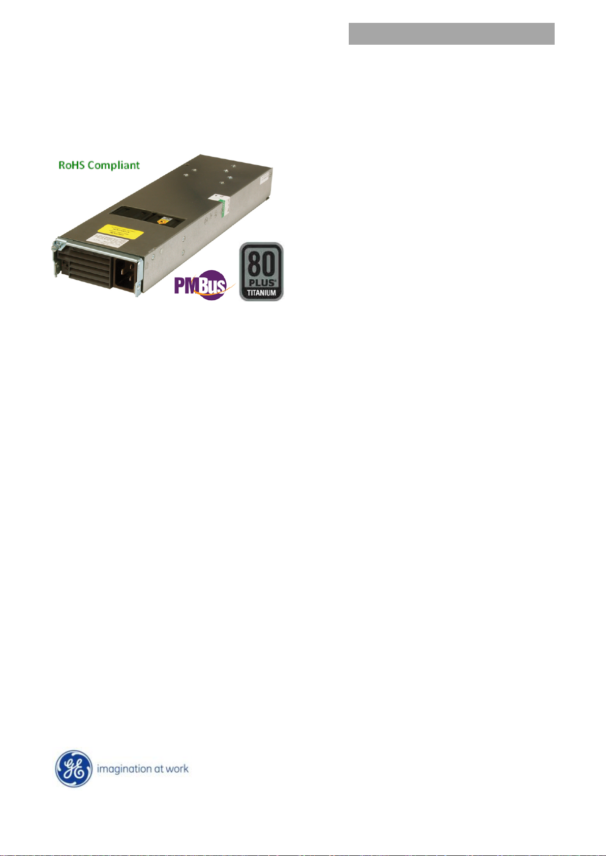
CAR2912TE series front-end
Preliminary Data Sheet
Features
• Efficiency: meets 80plus “Titanium” criteria
• Universal input with PFC
• Constant power characteristic
• 2 front panel LEDs: 1-input;2-[DC_OK, fault, warning]
• ON/OFF control of the 12Vdc output
• Remote sense on the 12Vdc output
Applications
• 12Vdc distributed power architectures
• Routers/ VoIP/Soft and other Telecom Switches
• Mid to high-end Servers, ATE Equipment
Targeted Countries
China, Taiwan, Japan, South Korea, Singapore
EU Countries
Brazil, Canada, Mexico, Argentina, USA
Description
• No minimum load requirements
• Active load sharing (single wire)
• Hot Plug-ability
• Standby orderable either as 3.3Vdc or 5Vdc @ 4A
• Auto recoverable OC & OT protection
• Operating temperature: -10 - 70°C (de-rated above 50°C)
• Digital status & control: dual/redundant PMBus™ serial
bus
• EN/IEC/UL60950-1 2
• EMI: class A FCC docket 20780 part 15, EN55022
• Meets EN6100 immunity and transient standards
• Shock & vibration: NEBS GR-63-CORE, level 3
nd
edition; UL, CSA, VDE , and CCC
The CAR2912TE Front-End provides highly efficient isolated power from worldwide input mains in a compact 1U
industry standard form factor. This power supply is ideal for applications where mid to light load efficiency is of key
importance in order to reduce system power consumption during ‘typical’ operational conditions.
The high-density, front-to-back airflow is designed for minimal space utilization and is highly expandable for future
2
growth. Dual/redundant, industry standard, PMBus™ compliant I
C communications busses offer a full range of
control and monitoring capabilities with sequential control from two independent sources
UL is a registered trademark of Underwriters Laboratories, Inc.
† CSA is a registered tradem ark of Canadian Standards Association.
‡ VDE is a trademark of Verband Deutscher Elektrotechniker e.V.
§ Intended for integration into end-user equipment. All the required procedures for CE marking of end-user equipment should be followed. (The CE mark is placed on selected products.)
** ISO is a registered trademark of the International Organization of Standards.
Page 2
GE
CAR2912TE series front-end
Input: 90Vac to 264Vac; Output: 12Vdc @ 2900W; 3.3 or 5Vdc @ 4A Standby
October 21, 2013
©2013 General Electric Company. All rights reserved.
Page 2
FIN
Efficiency (T
=25°C, VO= 12V) VIN
Power Factor (VIN=115/230VAC), IO= 50% I
IO= I
0.98
0.99
Holdup time (Vout≥ 10.8VDC, Tamb 25°C, IO=I
) Vin= 230VAC
VIN= 100VAC
12
20
12Vdc MAIN OUTPUT
Set point
11.9
12.00
12.1
V
DC
Preliminary Data Sheet
Absolute Maximum Ratings
Stresses in excess of the absolute maximum ratings can cause permanent damage to the device. These are absolute stress ratings only, functional
operation of the device is not implied at these or any other conditions in excess of those given in the operations sections of the data sheet. Exposure
to absolute maximum ratings for extended periods can adversely affect the device reliability.
Parameter Symbol Min Max Unit
Input Voltage: Continuous VIN 0 264 VAC
Operating Ambient Temperature TA -10 701 °C
Storage Temperature Tstg -40 85 °C
I/O Isolation voltage to Frame (100% factory Hi-Pot tested) 2121 VDC
Electrical Specifications
Unless otherwise indicated, specifications apply over all operating input voltage, load, and temperature conditions.
INPUT
Parameter Symbol Min Typ Max Unit
Operational Range VIN 85 115/230 264 VAC
Frequency Range (ETSI 300-132-1 recommendation)
Main Output Turn OFF
V
IN
Hysteresis between turn OFF and turn ON 5
Maximum Input Current (VO= V
VIN= 208VAC
Cold Start Inrush Current (Excluding x-caps, 25°C, <10ms,
per ETSI 300-132)
amb
O, set
, IO=I
) VIN= 100VAC
O, max
I
IN
I
IN
100% load
50% load
20% load
η
10% load
O, max
O, max
O, max
PF
T
Early warning prior to output falling below regulation2 2
Ride through T 10
Leakage Current (VIN= 250VAC, FIN = 60Hz) I
Isolation Input/Output
IN
Input/Frame 2121 V
Output/Frame 100 V
47 50/60 63 Hz
70 80
16.3
15.9
40 A
115V / 230V
92 / 93.5
93 / 96
%
92 / 94.0
88 / 91.5
3 mA
3000 V
VAC Main Outptut Turn ON 75 85
A
PEAK
ms
AC
AC
DC
DC
RMS
Parameter Symbol Min Typ Max Unit
Output Power 180 – 264 / 90-132 Vac
V
≤ 90V
AC
AC
Overall regulation (load, temperature) -2 +2 %
W
V
O
0 - 2900/1400 W
0 - 1200 W
1
Power derated above 50°C, see environmental section
2
Measured by the DC_OK signal going LO prior to the output decaying below 10.8Vdc
Page 3
GE
CAR2912TE series front-end
Input: 90Vac to 264Vac; Output: 12Vdc @ 2900W; 3.3 or 5Vdc @ 4A Standby
October 21, 2013
©2013 General Electric Company. All rights reserved.
Page 3
P-P
Turn-ON delay
T 2 sec
Programmable range (hardware & software)
10.8 13.2
V
Current limit, Hiccup (programmable level)
110 130
% of FL
Ripple and noise
50
mV
Output current
IO 0 4
A
Parameter
Min
Typ
Max
Units
Notes
Full load, ; MTBF per SR232 Reliability protection for
Service Life
10 Yrs
Full load, excluding fans
Weight
Preliminary Data Sheet
12Vdc MAIN OUTPUT (continued)
Parameter Symbol Min Typ Max Unit
Ripple and noise3 -120 120
Turn-ON overshoot +3 %
mV
ON/OFF delay time
Turn-ON rise time (10 – 90% of V
)
out
Transient response 50% step [10%-60%, 50% - 100%]
(dI/dt – 1A/µs, recovery 300µs)
Overvoltage protection, latched
(recovery by cycling OFF/ON via hardware or software)
Output current 180 ≥ VIN ≥ 264
90 ≥ V
≥ 132
IN
V
O
I
O
40 ms
50 ms
-5 +5 %V
13.8 14.8 15.8
0
242
117
O
DC
V
DC
A
DC
Active current share -5 +5 % of FL
STANDBY OUTPUT
Parameter Symbol Min Typ Max Unit
Set point VO 3.3 / 5.0 V
Overall regulation (load, temperature, aging) VO -5 +5 %
Overload protection - 110 150 % of FL
Isolation Output/Frame 100
DC
P-P
DC
V
DC
General Specifications
Reliability, 25°C
50°C
320,000
100,000
Hrs
electronic equipment, method I, case III,
Feature Specifications
Unless otherwise indicated, specifications apply over all operating input voltage, resistive load, and temperature conditions. See
Control and Status for additional information.
Parameter Symbol Min Typ Max Unit
ON/OFF (Needs to be pulled HI via an external resistor)
Logic High (Module ON) I
V
Logic Low (Module OFF) I
V
IH
IH
IL
IL
0.7V
DD
0
20 µA
12 V
4 mA
0.8 VDC
DC
3
Measured across a 10µf tantalum and a 0.1µf ceramic capacitors in parallel. 20MHz bandwidth
Page 4

GE
CAR2912TE series front-end
Input: 90Vac to 264Vac; Output: 12Vdc @ 2900W; 3.3 or 5Vdc @ 4A Standby
October 21, 2013
©2013 General Electric Company. All rights reserved.
Page 4
(pulled up internally to V
by a 10kΩ resistor)
Over Temperature Warning (pulled up internally to V
by a
10kΩ resistor)
Fault (pulled up internally to V
by a 10kΩ resistor)
Logic Low (Power supply is present)
VIL
0 0.1
VDC
Preliminary Data Sheet
Feature Specifications (continued)
Parameter Symbol Min Typ Max Unit
Output Voltage programming (Vprog)
Equation: Vout = 10.8 + (Vprog * 0.96)
Vprog range V
Programmed output voltage range Vo
Voltage adjustment resolution Vo
Output configured to 13.2Vdc V
Output configured to the 12Vdc set-point V
Interlock [short pin controlling presence of the 12VDC output]
stdby
12V output ON VI
12V output OFF VI
AC-OK (pulled up internally to V
by a 10kΩ resistor)
stdby
Logic High (Input within normal range) I
V
Logic Low (Input out of range) I
V
DC-OK (pulled up internally to V
Logic High (Output voltage is present; V
by a 10kΩ resistor)
stdby
≥ 10.7Vdc) I
OUT
V
Logic Low (Output voltage is not present; V
≤ 10.2V
OUT
) I
DC
V
stdby
prog
0
10.8
2.5 3.0 VDC
prog
prog
3.0
10
2.5 VDC
13.2 VDC
0.7 V
stdby
0
V
VDC
stdby
0.4 VDC
OH
OL
OH
OL
0.7 V
stdby
0
20 µA
V
VDC
stdby
4 mA
0.4 VDC
OH
OL
OH
OL
0.7 V
stdby
0
20 µA
VDC
V
stdby
4 mA
0.4 VDC
mVDC
VDC
Logic High (temperature within normal range) I
V
Logic Low (temperature is too high) I
V
OH
OH
OL
OL
0.7 V
stdby
0
20 µA
V
VDC
stdby
4 mA
0.4 VDC
Delayed shutdown after Logic Low transition Tdelay 10 sec
stdby
Logic High (No fault is present) I
V
Logic Low (Fault is present) I
V
PS Present [internally connected to Output return]
(Needs to be pulled HI via an external resistor)
Logic High (Power supply is not plugged in)
8V_INT (no components should be connected to this pin)
OH
OL
OH
OL
0.7 V
stdby
0
20 µA
V
VDC
stdby
4 mA
0.4 VDC
Page 5
GE
CAR2912TE series front-end
Input: 90Vac to 264Vac; Output: 12Vdc @ 2900W; 3.3 or 5Vdc @ 4A Standby
October 21, 2013
©2013 General Electric Company. All rights reserved.
Page 5
Preliminary Data Sheet
Digital Interface Specifications
Parameter Conditions Symbol Min Typ Max Unit
PMBus Signal Interface Characteristics4
Input Logic High Voltage (CLK, DATA) VIH 0.7V
Input Logic Low Voltage (CLK, DATA) VIL 0 0.8 V
Input high sourced current (CLK, DATA) IIH 0 10 μA
Output Low sink Voltage (CLK, DATA, SMBALERT#) IO=5mA VOL 0.4 V
Output Low sink current (CLK, DATA, SMBALERT#) IOL 5 mA
Output High open drain leakage current (CLK,DATA,
SMBALERT#)
PMBus Operating frequency range Slave Mode FPMB 10 400 kHz
Measurement System Characteristics
Clock stretching
I
measurement range
OUT
I
measurement accuracy 25°C
OUT
V
measurement range
OUT
V
measurement accuracy
OUT
Temp measurement range
Temp measurement accuracy5
IIN measurement range Direct
IIN measurement accuracy
VIN measurement range
VIN measurement accuracy
PIN measurement range
PIN measurement accuracy
Fan Speed measurement range
Fan Speed measurement accuracy
Fan speed control range
=3.6V I
V
O
Direct
Direct
Direct
Direct
Direct
Direct
Direct
OH
tSTRETCH 25 ms
I
RNG
I
OUT
V
OUT(rng)
V
OUT(acc)
Temp
Temp
I
IN(rng)
I
IN(acc)
V
IN(rng)
V
IN(acc)
P
N(rng)
P
IN(acc)
(rng)
(acc)
DD
0 10 μA
0 242 A
-2.5 +2.5 % of FL
0 14 V
-1 +1 %
0 125
-3 +3
0 18 AAC
-5 +5 %
0 320 VAC
-2 +2 %
0 3000 W
-3 +3 %
0 30k RPM
-10 10 %
0 100 %
3.6 V
°C
°C
4
Clock, Data, and SMBAlert need to be pulled up to VDD externally.
5
Temperature accuracy reduces non-linearly with decreasing temperature
Page 6
GE
CAR2912TE series front-end
Input: 90Vac to 264Vac; Output: 12Vdc @ 2900W; 3.3 or 5Vdc @ 4A Standby
October 21, 2013
©2013 General Electric Company. All rights reserved.
Page 6
Parameter
Min
Typ
Max
Units
Notes
Storage Temperature
-40 85
°C
Operating Altitude
2250/7382
m/ft
Non-operating Altitude
8200/30k
m / ft
Power Derating with Altitude
2.0
Above 1524 m/5000 ft
Acoustic noise
55
Full load
Shock and Vibration acceleration
2.4
Grms
Meet IPC-9592B Class II
Environmental Specifications
Preliminary Data Sheet
Ambient Temperature
Power Derating with Temperature 2.5
6
-10
70 °C
%/°C
Derated above 50°C
50°C to 70°C
°C/301 m
°C/1000 ft
45
dbA
Half load
Over Temperature Protection 125/110 °C Shutdown / restart
Humidity
Operating
Storage
30
10
95
% Relative humidity, non-condensing
95
EMC Compliance
Parameter Criteria Standard Level Test
Conducted emissions EN55022, FCC Docket 20780 part 15, subpart J
AC input
Radiated emissions** EN55022 A* 30 – 10000MHz
Voltage dips EN61000-4-11 B -30%, 10ms
AC input
immunity
Enclosure
immunity
Voltage surge EN61000-4-5 A 4kV, 1.2/50µs, common mode
Fast transients EN61000-4-4 B 5/50ns, 2kV (common mode)
Conducted RF fields EN61000-4-6 A 130dBµV, 0.15-80MHz, 80% AM
Radiated RF fields EN61000-4-3 A 10V/m, 80-1000MHz, 80% AM
ESD EN61000-4-2 B 4kV contact, 8kV air
EN61000-3-2
ENV 50140 A
A* 0.15 – 30MHz
0 – 2 KHz
B -60%, 100ms
B -100%, 5sec
A 2kV, 1.2/50µs, differential mode
* Note: Contact the factory for a recommended external EMI filter to meet Class B emissions
Radiated emissions compliance is contingent upon the final system configuration.
**
6
Designed to start at an ambient down to -40°C; meet spec after ≅ 30 min warm up period, may not meet operational limits below -10°C.
Page 7

GE
CAR2912TE series front-end
Input: 90Vac to 264Vac; Output: 12Vdc @ 2900W; 3.3 or 5Vdc @ 4A Standby
October 21, 2013
©2013 General Electric Company. All rights reserved.
Page 7
Device
Address
Address Bit Assignments
(Most to Least Significant)
7 6 5 4 3 2 1
0
MCU
C or Dx
1 1 0
A3
A2
A1
A0
R/W
Broadcast
00
0 0 0 0 0 0 0
0
ARA7
12
0 0 0 1 1 0 0
1
MSB LSB
Control and Status
Preliminary Data Sheet
interrupted, for example if input power or bias power is
recycled.
Control hierarchy: Some features, such as output voltage,
can be controlled both through hardware and firmware. For
example, the output voltage is controlled both by a signal pin
(Vprog) and a PMBus command, (OPERATION) .
Unless otherwise noted, the signal pin controls the feature
until the firmware command is executed. However, once the
firmware command has been executed, the signal pin is
ignored. In the above example, the power supply will no
longer ‘listen’ to the Vprog pin if the OPERATION command
has been executed.
In summary, Vprog is utilized for initialized configuration of
the output voltage and to change the output voltage when
PMBus is not used for that function.
Analog controls: Details of analog controls are provided in
this data sheet under Feature Specifications.
Common ground: All signals and outputs are referenced to
Output return.
Control Signals
Device address: Address bits A3, A2, A1, A0 configure the
specific address of the power supply. With these four bits, up
to sixteen (16) modules to be addressed on a single I²C bus.
The pins are pulled HI internal to the power supply. For a logic
LO these pins should be connected to ‘Output Return’. The
least significant bit x (LSB) of the address byte is set to either
write [0] or read [1]. A write command instructs the power
supply. A read command accesses information from the
power supply.
When bias power is recycled to the controller the controller
restarts into its default configuration, programmed to set the
output as instructed by the V
software commanded settings permanently override the
margin setting. As an example of an effective use of
hardware programming prior to the availability of software
based controls is to add a resistor between V
Output_return. This is a way of changing the factory set point
of the front-end to whatever voltage level is desired by the
user during initial start-up.
Load share (I
generated and acted upon automatically by power supplies
connected in parallel. I
other for power supplies, if active current share among the
power supplies is desired. No resistors or capacitors should
get connected to this pin.
Remote ON/OFF: Controls the presence of the main 12Vdc
output voltage. This is an open collector signal that needs to
be pulled HI externally through a resistor. A logic HI turns ON
the main output.
A turn OFF command either through this signal (ON/OFF) or
firmware commanded would turn OFF the 12V output.
Interlock: This is a short signal pin that controls the presence
of the 12Vdc main output. This pin should be connected to
‘output return’ on the system side of the output connector.
The short pin ensures that no arcing or contact damage
occurs during the insertion/extraction process.
8V_INT: Provides the ability to back_bias a front-end that lost
input power thus maintaining the ability to communicate with
a remote controller. This pin should be interconnected among
units in a system.
): This is a single wire analog signal that is
share
share
pin. Again, subsequent
prog
and
prog
pins should be connected to each
Status signals
See Feature Specifications for additional information
AC OK: A TTL compatible status signal representing whether
the input voltage is within the anticipated range. This signal
Voltage programming (V
signal can vary the output voltage ± 10% from 10.8Vdc to
13.2Vdc.
Hardware voltage programming controls the output voltage
until a software margin command is executed. Software
voltage programming permanently overrides the hardware
margin setting and the power supply no longer listens to any
hardware margin settings until power to the controller is
7
Implement if feasible, this is a ‘read’ only address
): An analog voltage on this
prog
needs to be pulled HI externally through a resistor.
DC OK: A TTL compatible status signal representing whether
the output voltage is present. This signal needs to be pulled HI
externally through a resistor.
Over temp warning: A TTL compatible status signal
representing whether an over temperature exists. This signal
needs to be pulled HI externally through a resistor.
If an over temperature should occur, this signal would pull LO
for approximately 10 seconds prior to shutting down the
power supply. In its default configuration, the unit would
Page 8
GE
CAR2912TE series front-end
Input: 90Vac to 264Vac; Output: 12Vdc @ 2900W; 3.3 or 5Vdc @ 4A Standby
October 21, 2013
©2013 General Electric Company. All rights reserved.
Page 8
Clock
Stretch
restart if internal temperatures recover within normal
operational levels. At that time the signal reverts back to its
open collector (HI) state.
Fault: This signal goes LO for any failure that requires rectifier
replacement. These faults may be due to:
• Fan failure
• Over-temperature warning
• Over-temperature shutdown
• Over-voltage shutdown
• Internal Rectifier Fault
PS Present: This signal notifies the system controller that a
power supply is physically present in the slot. This signal pin is
pulled down to Output_return by the power supply.
Serial Bus Communications
The I²C interface facilitates the monitoring and control of
various operating parameters within the unit and transmits
these on demand over an industry standard I²C Serial bus.
All signals are referenced to ‘Output Return’.
Pull-up resistors: The clock, data, and SMBusAlert# lines do
not have any internal pull-up resistors inside the power
supply. The customer is responsible for ensuring that the
transmission impedance of the communications lines
complies with I2C and SMBus standards.
Serial Clock (SCL): The clock pulses on this line are generated
by the host that initiates communications across the I²C
Serial bus. This signal needs to be pulled HI externally through
a resistor as necessary to ensure that rise and fall time timing
and the maximum sink current is in compliance to the I²C
/SMBus specifications.
Serial Data (SDA): This line is a bi-directional data line. This
signal needs to be pulled HI externally through a resistor as
necessary to ensure that rise and fall time timing and the
maximum sink current is in compliance to the I²C /SMBus
specifications.
SMBUSAlert#: This hardware signal pin is normally HI. When
asserted (logic LO) it signifies to the system controller that the
state of the power supply has changed or that
communication errors occurred.
Preliminary Data Sheet
communications error alarms (PEC error, data error,
command error). If the alarm state is still present the status
and alarm registers get reset into their alarm state, however,
the SMBAlert# does not assert again.
‘Manufacturer Specific’ commands are used to support
instructions that are not offered by the PMBus™ specification.
All communication over the PMBus interface must support
Packet Error Checking (PEC). The PMBus master must
generate the correct PEC byte for all transactions, and check
the PEC byte returned by the power supply.
Non-volatile memory is used to store configuration settings.
Not all settings programmed into the device are
automatically saved into this non-volatile memory. Only those
specifically identified as capable of being stored can be
saved. (see the Table of Commands for which command
parameters can be saved to non-volatile storage).
Non-supported commands: Non supported commands are
flagged by setting the appropriate STATUS bit and issuing an
SMBAlert# to the ‘host’ controller. If a non-supported read is
requested the power supply will return 0x00h for data.
Data out-of-range: The power supply validates data settings
and sets the data out-of-range bit and SMBAlert# if the data
is not within acceptable range.
Master/Slave: The ‘host controller’ is always the MASTER.
Power supplies are always SLAVES. SLAVES cannot initiate
communications or toggle the Clock. SLAVES also must
respond expeditiously at the command of the MASTER as
required by the clock pulses generated by the MASTER.
Clock stretching: The ‘slave’ µController inside the power
supply may initiate clock stretching if it is busy and it desires
to delay the initiation of any further communications. During
the clock stretch the ‘slave’ may keep the clock LO until it is
ready to receive further instructions from the host controller.
The maximum clock stretch interval is 25ms.
The host controller needs to recognize this clock stretching,
and refrain from issuing the next clock signal, until the clock
line is released, or it needs to delay the next clock pulse
beyond the clock stretch interval of the power supply.
Digital Feature Descriptions
PMBus™ compliance: The power supply is compliant to the
Power Management Bus (PMBus™) rev1.2 requirements with
the exception of response to the Alert Response Address (ARA)
command. This is further explained under the section on ARA.
The power supply clears the STATUS and ALARM registers and
the SMBAlert# signal after a successful read back of the
information in these registers, with the exception of
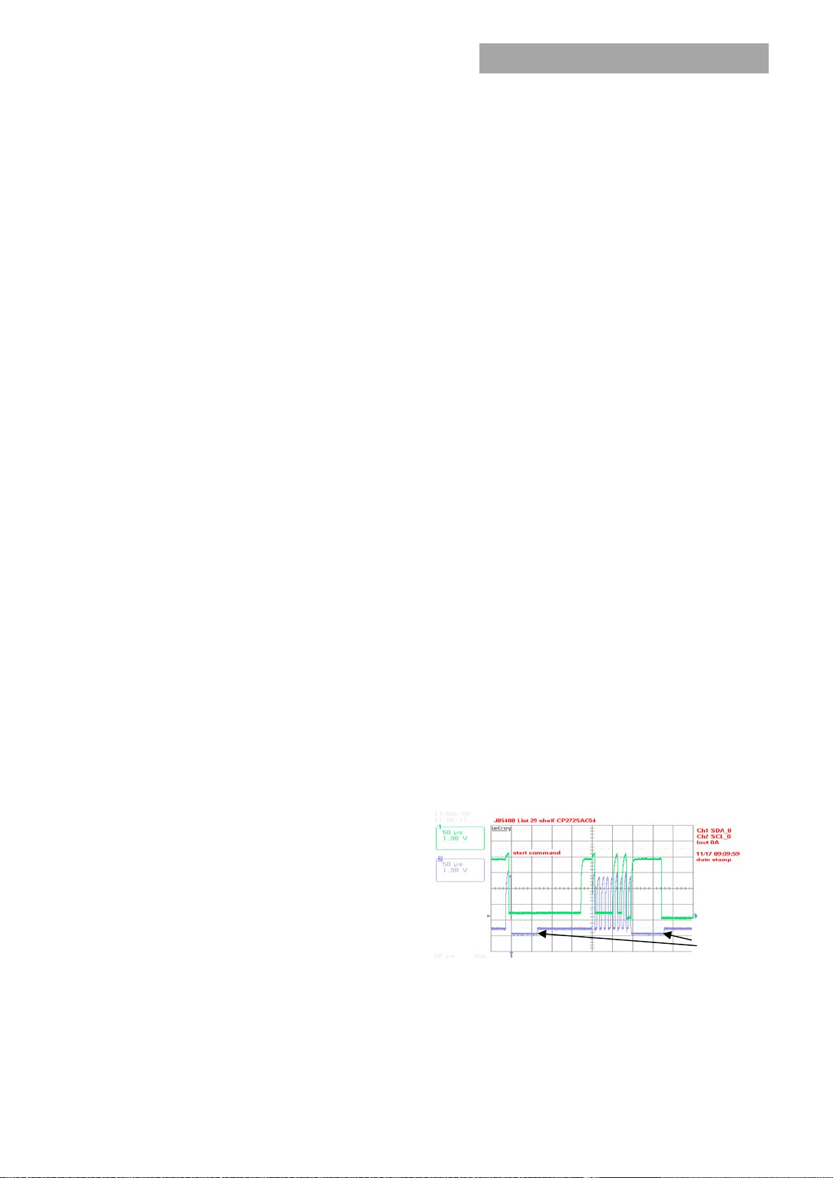
Figure 1. Example waveforms showing clock stretching.
Note that clock stretching can only be performed after
completion of transmission of the 9
being the START command.
th
ACK bit, the exception
Page 9

GE
CAR2912TE series front-end
Input: 90Vac to 264Vac; Output: 12Vdc @ 2900W; 3.3 or 5Vdc @ 4A Standby
October 21, 2013
©2013 General Electric Company. All rights reserved.
Page 9
I²C Bus Lock-Up detection: The device will abort any
transaction and drop off the bus if it detects the bus being
held low for more than 35ms.
Communications speed: Both 100kHz and 400kHz clock
rates are supported. The power supplies default to the
100kHz clock rate. The minimum clock speed specified by
SMBus is 10 kHz.
Packet Error Checking (PEC): The power supply will not
respond to commands without the trailing PEC because the
integrity of communications is compromised without packet
error correction deployment.
PEC is a CRC-8 error-checking byte, based on the polynomial
8
+ x2 + x + 1, in compliance with PMBus™
C(x) = x
requirements. The calculation is performed on all message
bytes, including the originating write address and command
bytes preceding read instructions. The PEC is appended to the
message by the device that supplied the last byte.
SMBAlert#: The power supply can issue SMBAlert# driven
from either its internal micro controller (µC) or from the I
bus master selector stage. That is, the SMBAlert# signal of the
internal µC funnels through the master selector stage that
buffers the SMBAlert# signal and splits the signal to the two
SMBAlert# signal pins exiting the power supply. In addition,
the master selector stage signals its own SMBAlert# request
to either of the two SMBAlert# signals when required.
The µC driven SMBAlert# signal informs the ‘master/host’
controller that either a STATE or ALARM change has occurred.
Normally this signal is HI. The signal will change to its LO level
if the power supply has changed states and the signal will be
latched LO until the power supply either receives a
‘clear_faults’ instruction as outlined below, or a read_status
(0xD0) or a status_word (0x79,) instructions are executed. If
the same alarm state is still present after the ‘clear_faults’
command has been received the status registers will revert
back into their alarm state but the SMBAlert# will not be
asserted. This response ensures that the ‘host’ controller
does not get bombarded by continuous SMBAlert# asserts for
the same fault. The ‘host’ will then be in a position to monitor
the power system for other events.
The signal will be triggered for any state change whether a
‘warning’ or a ‘fault’, including the following conditions;
• VIN under or over voltage
• Vout under or over voltage
• IOUT over current
• Over Temperature
• Fan Failure
• Communication error
• PEC error
• Invalid command
• Detected internal faults
2
C
Preliminary Data Sheet
• The main output recycled (turned OFF and then ON) via
the ON/OFF signal pin
• The main output recycled (turned OFF and then ON) by
the OPERATION command
• Bias power to the processor is recycled
Re-initialization: The I
no activity is detected on the bus for 5 seconds. Reinitialization is designed to guarantee that the I2C µController
does not hang up the bus. Although this rate is longer than
the timing requirements specified in the SMBus specification,
it had to be extended in order to ensure that a re-initialization
would not occur under normal transmission rates. During the
few µseconds required to accomplish re-initialization the I
µController may not recognize a command sent to it. (i.e. a
start condition).
Read back delay: The power supply issues the SMBAlert #
notification as soon as the first state change occurred. During
an event a number of different states can be transitioned to
before the final event occurs. If a read back is implemented
rapidly by the host a successive SMBAlert# could be triggered
by the transitioning state of the power supply. In order to
avoid successive SMBAlert# s and read back and also to
avoid reading a transitioning state, it is prudent to wait more
than 2 seconds after the receipt of an SMBAlert# before
executing a read back. This delay will ensure that only the
final state of the power supply is captured.
Successive read backs: Successive read backs to the power
supply should not be attempted at intervals faster than every
one second. This time interval is sufficient for the internal
processors to update their data base so that successive
reads provide fresh data.
Global Broadcast: This is a powerful command because it
instruct all power supplies to respond simultaneously. A read
instruction should never be accessed globally. The power
supply should issue an ‘invalid command’ state if a ‘read’ is
attempted globally.
For example, changing the ‘system’ output voltage requires
the global broadcast so that all paralleled power supplies
change their output simultaneously. This command can also
turn OFF the ‘main’ output or turn ON the ‘main’ output of all
power supplies simultaneously. Unfortunately, this command
does have a side effect. Only a single power supply needs to
pull down the ninth acknowledge bit. To be certain that each
power supply responded to the global instruction, a READ
instruction should be executed to each power supply to verify
that the command properly executed. The GLOBAL
BROADCAST command should only be executed for write
instructions to slave devices.
2
C code is programmed to re-initialize if
2
C
The power supply will clear the SMBusAlert# signal (release
the signal to its HI state) upon the following events:
• Receiving a CLEAR_FAULTS command
Page 10

GE
CAR2912TE series front-end
Input: 90Vac to 264Vac; Output: 12Vdc @ 2900W; 3.3 or 5Vdc @ 4A Standby
October 21, 2013
©2013 General Electric Company. All rights reserved.
Page 10
1 8 1 8 1 S Slave address
Wr A Command Code
A 8 1 8
1 8 1
1
Low data byte
A
High data byte
A
PEC A P
1 7 1 1 8
1
S
Slave address
Wr A Command Code
A 1 7
1 1 8
1
Sr
Slave Address
Rd A LSB
A
8 1 8
1 1 MSB A PEC
No-ack
P
µC
DSP
Bidirectional
Isolator
I2C_0
2
Alert Response Address (ARA): This feature enables the
‘master’ to rapidly determine which ‘slave’ power supply
triggered the SMBAlert signal without having to poll each
power supply one at a time. During normal operation the
power supply activates (pulls down LO) the Alert signal line
indicating that it needs attention when a ‘state’ change
occurs. The master can determine who pulled the ‘alert’ line
by sending out the alert-response-address, address 12b, with
a ‘read’ instruction. If the power supply triggered the ‘alert’ it
should respond back with its address. The instruction takes
the form below;
1 8 1 8 1 8 1 1
S ARA address Rd A My address A PEC A P
If during the ARA response multiple power supplies send out
their addresses, then the actual address received by the
master is the lowest address from the combinations of those
power supplies that responded.
The ‘my address’ field contains the address of the power
supply in the 7 most significant bits (msb) of the byte. The lsb
of the byte is a don’t care, it could be a 0 or a 1. For more
information refer to the SMBus specification.
The µC does not have the ability to listen to the actual
address that is sent over the bus, if multiple ‘slaves’ respond
simultaneously, and therefore it does not clear its SMBAlert
line. The host should read the status of the power supply
whose address was actually sent across the bus. Reading
either the read_status [0 x D0] or status_word [0 x 79] would
clear the SMBALert line of the power supply that was
addressed. The power supply will not re-assert the SMBAlert
line unless the status states actually changed.
If the SMBAlert line is still asserted, the host should send out
an ARA request again and find out who else asserted
SMBAlert. This process needs to continue until the SMBAlert is
released which is a clear indication that all power supplies
that asserted SMBAlert have had their status states read
back.
2
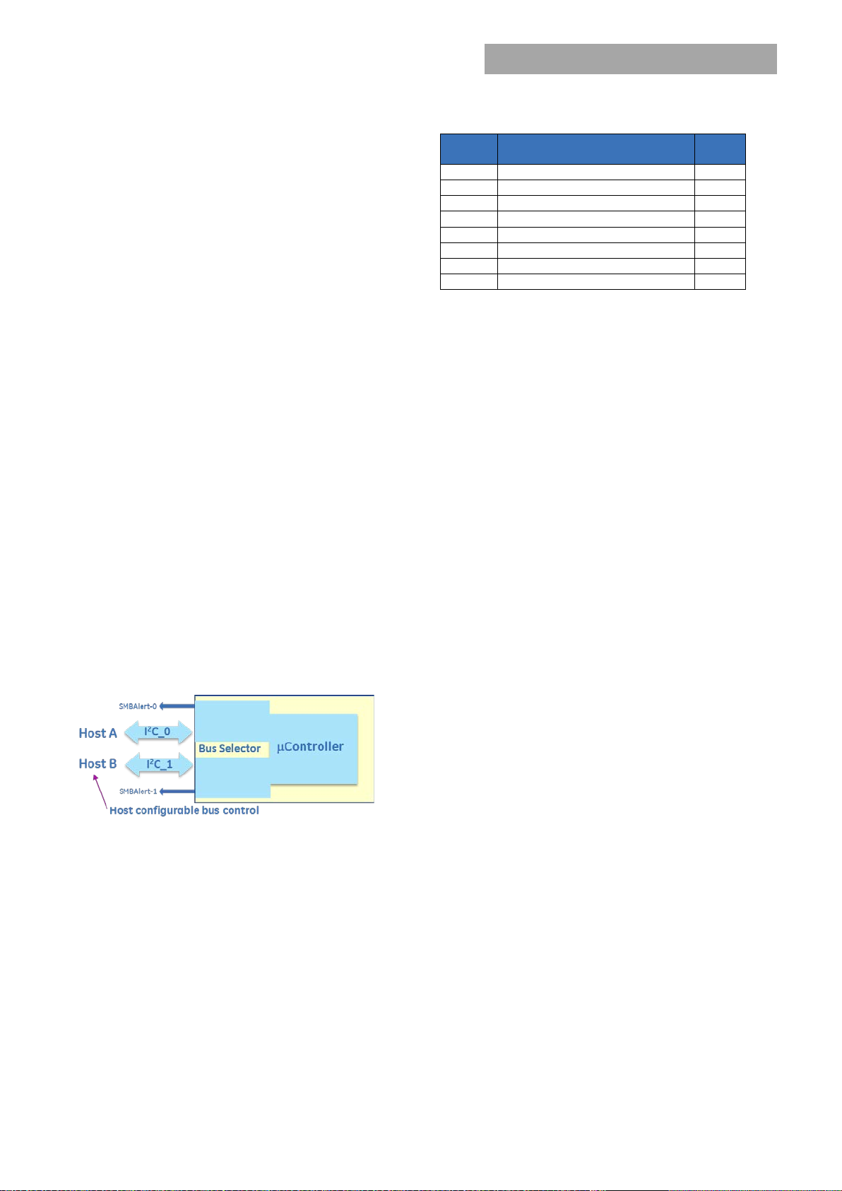
Dual, redundant buses: Two independent I
C lines provide
true communications bus redundancy and allow two
independent controllers to sequentially control the power
supply. For example, a short or an open connection in one of
2
C lines does not affect communications capability on the
the I
2
other I
C line. Failure of a ‘master’ controller does not affect
the power supplies and the second ‘master’ can take over
control at any time.
Conceptually a Digital Signal Processor (DSP) referenced to
Vout(-) of the power supply provides secondary control. A
Bidirectional Isolator provides the required isolation between
power GRD, Vout(-) and signal GRD (Logic_GRD). A secondary
micro controller provides instructions to and receives
operational data from the DSP. The secondary micro
controller also controls the communications over two
independent I2C lines to two independent system controllers.
Preliminary Data Sheet
The secondary micro controller is designed to default to I2C_0
when powered up. If only a single system controller is utilized,
it should be connected to I2C_0. In this case the I2C_1 line is
totally transparent as if it does not exist.
If two independent system controllers are utilized, then one of
them should be connected to I2C_0 and the other to I2C_1.
At power up the master connected to I2C_0 has control of the
bus. See the section on Dual Master Control for further
description of this feature.
PMBusTM Commands
Standard instruction: Up to two bytes of data may follow an
instruction depending on the required data content. Analog
data is always transmitted as LSB followed by MSB. PEC is
optional and includes the address and data fields.
Master to Slave Slave to Master
SMBUS annotations; S – Start , Wr – Write, Sr – re-Start, Rd
– Read,
A – Acknowledge, NA – not-acknowledged, P – Stop
Standard READ:
request depending on the required data content. Analog
data is always transmitted as LSB followed by MSB. PEC is
mandatory and includes the address and data fields
Block communications: When writing or reading more than
two bytes of data at a time BLOCK instructions for WRITE and
READ commands are used instead of the Standard
Instructions above to write or read any number of bytes
greater than two.
Up to two bytes of data may follow a READ
.
Page 11
GE
CAR2912TE series front-end
Input: 90Vac to 264Vac; Output: 12Vdc @ 2900W; 3.3 or 5Vdc @ 4A Standby
October 21, 2013
©2013 General Electric Company. All rights reserved.
Page 11
1 7 1 1 8 1 S Slave address
Wr A
Command Code
A 8 1 8 1 8 1 Byte count = N
A
Data 1
A
Data 2
A 8 1 8 1 8 1 1 ……….
A
Data 48
A
PEC
A
P
1 7 1 1 8 1 S Slave address
Wr A
Command Code
A
1 7 1 1 Sr
Slave Address
Rd A 8 1 8 1 8 1 Byte count = N
A
Data 1
A
Data 2
A
8 1 8 1 8 1 1
……….
A
Data 48 A PEC
NoAck
P
FUNCTION
Operation
m b R
Output voltage
Output voltage shutdown
Write / read
TBD 0 0
Output Current
read
TBD 0 0
Temperature
read
1 0 0
Input Voltage
read
1
75 0 Input Power
read
1 0 0
Fan Speed setting ( % )
read
1 0 0
Fan speed in RPM
read
100 0 0
Command
Comments
Vout_OV_fault_response (0x41)
Only latched (0x80) is supported
Non-
Operation
0x01 1 yes
Clear_Faults
0x03 0
Write _Protect
0x10 1 no
Vout_mode
0x20 1
Vout_command
0x21 2 yes
Vin_ON
0x35 2 no
Vin_OFF
0x36 2 no
Vout_OV_fault_limit
0x40 2 yes
Vout_OV_fault_response
0x41 1 yes
Vout_OV_warn_limit
0x42 2 yes
Vout_UV_warn_limit
0x43 2 yes
Iout_OC_fault_limit
0x46 2 yes
Iout_OC_warn_limit
0x4A 2 yes
OT_fault_limit
0x4F 2 yes
OT_fault_response10
0x50 1 yes
Vin_OV_fault-response
0x56 1 yes
Vin_OV_warn_limit
0x57 2 yes
Vin_UV_warn_limit
0x58 2 yes
Vin_UV_fault_limit
0x59 2 yes
Status_word (+ byte)
0x79 1
Status_Vout
0x7A 1
Status_Iout
0x7B 1
Status_Input
0x7C 1
Read_Iin
0x89 2
Block write format:
Preliminary Data Sheet
PMBusTM Command set:
Non-supported commands are annunciated.
Block read format:
Direct mode data format: The Direct Mode data format is
R
supported, where y = [ mX + b ] x 10
. In the equation, y is the
data value from the controller and x is the ‘real’ value either
being set or returned.
For example, to set the output voltage to TBDVDC, Multiply the
desired set point by the m constant, TBD. Convert this binary
number to its hex equivalent: BBBBBBB. The result is sent
BBBBBB first, then BBBBB.
Hex
Command
Restore_default_all 0x12 0
Store_default_code 0x13 0 yes
Restore_default_code 0x14 0
Fan_config_1_2 0x3A 1 yes
Fan_command_1 0x3B 2
Vout_UV_fault_limit 0x44 2 yes
Vout_UV_fault_response8 0x45 1 yes
Iout_OC_fault_response9 0x47 1 yes
Code
Data
Field
Volatile
Memory
Storage
The constants are
Standard features
The commands below are ‘read only’. They cannot be modified.
ON_OFF_CONFIG (0x02) Both the CNTL pin, enabling or
disabling the output, and the
OPERATION command are
supported. Other options are not
supported.
CAPABILITY (0x19) 400KHz, SMBALERT
PMBus revision (0x98) 1.2
OT_warn_limit 0x51 2 yes
Vin_OV_fault_limit 0x55 2 yes
Vin_UV_fault_response 0x5A 1 yes
Status_byte 0x78 1
Status_temperature 0x7D 1
Status_CML 0x7E 1
Read_Vin 0x88 2
8
Only latched (0x80) or restart (0xC0) are supported
9
Only latched (0xC0) or hiccup (0xF8) are supported
10
Only latched (0x80) or restart (0xC0) are supported
Page 12

GE
CAR2912TE series front-end
Input: 90Vac to 264Vac; Output: 12Vdc @ 2900W; 3.3 or 5Vdc @ 4A Standby
October 21, 2013
©2013 General Electric Company. All rights reserved.
Page 12
Non-
Read_Vout
0x8B 2
Read_temperature_2
0x8E 2
Read_fan_speed_1
0x90 2
Read_fan_speed_2
0x91 2
Read_Pin
0x97 2
Mfr_revision
0x9B 4
Mfr_serial
0x9E
15
Read_status
0xD0
10
Read_input_string
0xD4 2
Read_firmware_rev
0xD5 3
Read_run_timer
0xD6 3
Stretch_LO_25ms
0XDA 0
Test Function
0xDF 1
Compatibility code
0xE0
20
Boot loader
0xE2 1
Data transfer
0xE3
≤32
FUNCTION
DATA BYTE
Unit ON
80
Unit OFF
00
FUNCTION
DATA BYTE
Enable all writes
00
Disable all writes except write_protect
80
Disable all writes except write_protect and
OPERATION
40
Mode
Bits [7:5]
Bits [4:0] (Parameter)
Command
Read_Iout 0x8C 2
Read_temperature_1 0x8D 2
Read_temperature_3 0x8F 2
Mfr_ID 0x99 5
Mfr_model 0x9A 16
Read_Status_state 0xD1 2
Read_Alarm_state 0xD2 2
Read_fan_speed 0XD3 4
Read Bus Status 0xD7 1
Take over bus control 0xD8
EEPROM Record 0xD9 128
Memory capability 0xE1 5
Hex
Code
Data
Field
Volatile
Memory
Storage
Preliminary Data Sheet
Clear_faults (0x03): This command clears all STATUS and
FAULT registers and resets the SMBAlert# line of both the
power supply and I
If a fault, or a STATUS needing attention, still persists after the
issuance of the clear_faults command, the specific registers
indicating the fault are reset and the specific SMBAlert# line is
activated again.
WRITE_PROTECT register (0x10): Used to control writing to
the PMBus device. The intent of this command is to provide
protection against accidental changes. All supported
command parameters may have their parameters read,
regardless of the write_protect settings. The contents of this
register can be stored to non-volatile memory using the
Store_default_code command. The default setting of this
register is disable_all_writes except write_protect 0x80h.
Restore_Default_All (0x12): Restores all register values and
responses to the default parameters set in the power supply.
Store_default_code (0x13): Changes the default setting of a
single register. In this fashion some protection is offered to
ensure that only those registers that are desired to be
changed are in fact changed.
Restore_default_code (0x14): Restore only a specific register
parameter to its default parameter.
Vout_mode (0x20): This is a ‘read only’ register. The upper
three bits specify the supported data format, in this case
Direct mode. The lower five bits are not used when direct
mode is specified since there are three variables for each
conversion.
2
C bus STATUS register.
Direct 010b Set to 00000b
Command Descriptions
Operation (0x01) : By default the Power supply is turned ON
at power up as long as Power ON/OFF signal pin is active HI.
The Operation command is used to turn the Power Supply ON
or OFF via the PMBus. The data byte below follows the
OPERATION command.
Vout_Command (0x21) : This command is used to change the
output voltage of the power supply.
Changing the output voltage should be performed
simultaneously to all power supplies operating in parallel
using the Global Address (Broadcast) feature. If only a single
power supply is instructed to change its output, it may
attempt to source all the required power which can cause
To RESET the power supply cycle the power supply OFF, wait
at least 2 seconds, and then turn back ON. All alarms and
shutdowns are cleared during a restart.
either a power limit or shutdown condition.
Software programming of output voltage permanently
overrides the set point voltage configured by the Vprog signal
pin. The program no longer looks at the ‘Vprog pin’ and will
not respond to any hardware voltage settings. If power is
removed from the µController it will reset itself into its default
Page 13

GE
CAR2912TE series front-end
Input: 90Vac to 264Vac; Output: 12Vdc @ 2900W; 3.3 or 5Vdc @ 4A Standby
October 21, 2013
©2013 General Electric Company. All rights reserved.
Page 13
configuration looking at the Vprog signal for output voltage
control. In many applications, the Vprog pin is used for
setting initial conditions, if different that the factory setting.
Software programming then takes over once I
communications are established.
To properly hot-plug a power supply into a live backplane, the
system generated voltage should get re-configured into
either the factory adjusted firmware level or the voltage level
reconfigured by the Vprog pin. Otherwise, the voltage state
of the plugged in power supply could be significantly different
than the powered system.
Voltage margin range: 10.8Vdc – 13.2 Vdc.
Vin_ON (0x35): This is a ‘read only’ register that informs the
controller at what input voltage level the power supply turns
ON. The default value is tabulated in the data section. The
value is contingent on whether the power supply operates in
the low_line or high_line mode.
Vin_OFF (0x36): This is a ‘read only’ register that informs the
controller at what input voltage level the power supply turns
OFF. The default value is tabulated in the data section. The
value is contingent on whether the power supply operates in
the low_line or high_line mode.
Fan_config_1_2 (0x3A) : This command allows the controller
to define whether the fan speed command is in duty cycle or
RPM. Both fans must be commanded simultaneously, either
by duty cycle or RPM. Mixing controls will result in a ‘data
error’. The tachometer pulses per revolution is not used.
Fan_command_1 (0x3B): This command instructs the power
supply to increase the speed of the fan. The transmitted data
byte represents the hex equivalent of the duty cycle in
percentage, i.e. 100% = 0 x 64h. The command can only
increase fan speed, it cannot instruct the power supply to
reduce the fan speed below what the power supply requires
for internal control.
Sending 00h tells the power supply to revert back to its
internal control.
Fan_command_2 (0x3C): not used in this power supply.
Issuing this command will result in ‘invalid command’.
Vout_OV_fault_limit (0x40): Sets the value at which the main
output voltage will shut down. The default OV_fault value is
set at 60Vdc. This level can be permanently changed and
stored in non-volatile memory.
Vout_OV_fault_response (0x41): This is a ‘read only’ register.
The only allowable state is a latched state after three retry
attempts.
An overvoltage shutdown is followed by three attempted
restarts, each successive restart delayed 1 second. If within a
1 minute window three attempted restarts failed, the unit will
latch OFF. If less than 3 shutdowns occur within the 1 minute
window then the count for latch OFF resets and the 1 minute
window starts all over again. This performance cannot be
changed.
2
C
Preliminary Data Sheet
Restart after a latched state: Either of four restart
mechanisms is available;
• The hardware pin Remote ON/OFF may be cycled OFF
and then ON.
• The unit may be commanded to restart via i2c through
the Operation command by first turning OFF then turning
ON .
• The third way to restart is to remove and reinsert the
unit.
• The fourth way is to turn OFF and then turn ON ac
power to the unit.
A successful restart clears all STATUS and ALARM registers.
A power system that is comprised of a number of power
supplies could have difficulty restarting after a shutdown
event because of the non-synchronized behavior of the
individual power supplies. Implementing the latch-off
mechanism permits a synchronized restart that guarantees
the simultaneous restart of the entire system.
A synchronous restart can be implemented by;
• Issuing a GLOBAL OFF and then a GLOBAL ON command
to all power supplies
• Toggling Off and then ON the Remote ON/OFF signal, if
this signal is paralleled among the power supplies.
• Removing and reapplying input commercial power to the
entire system.
The power supplies should be OFF for at least 20 – 30
seconds in order to discharge all internal bias supplies and
reset the soft start circuitry of the individual power supplies.
Vout_OV_warn_limit (0x42): Sets the value at which a
warning will be issued that the output voltage is too high. The
default OV_warn limit is set at 56Vdc. Exceeding the warning
value will set the Alert# signal. This level can be permanently
changed and stored in non-volatile memory.
Vout_UV_warn_limit (0x43): Sets the value at which a
warning will be issued that the output voltage is too low. The
default UV_warning limit is set at 41Vdc. Reduction below the
warning value will set the Alert# signal. This level can be
permanently changed and stored in non-volatile memory.
Vout_UV_fault_limit (0x44): Sets the value at which the
power supply will shut down if the output gets below this
level. The default UV_fault limit is set at 39Vdc. This register is
masked if the UV is caused by interruption of the input
voltage to the power supply. This level can be permanently
changed and stored in non-volatile memory.
Vout_UV_fault_response (0x45): Sets the response if the
output voltage falls below the UV_fault_limit. The default
UV_fault_response is restart (0xC0). The only two allowable
states are latched (0x80) and restart (0xC0). The default
response state can be permanently changed and stored in
non-volatile memory.
Page 14

GE
CAR2912TE series front-end
Input: 90Vac to 264Vac; Output: 12Vdc @ 2900W; 3.3 or 5Vdc @ 4A Standby
October 21, 2013
©2013 General Electric Company. All rights reserved.
Page 14
Bit
Position
Default
Value
7 X 0
6
OFF
0
5
VOUT Overvoltage
0 4 IOUT Overcurrent
0
3
VIN Undervoltage
0
2
Temperature
0 1 CML (Comm. Memory Fault)
0
0
None of the above
0
Bit
Position
Default
Value
7
VOUT fault or warning
0
6
IOUT fault or warning
0
5
INPUT
0
4
MFR SPECIFIC
0
3
nPOWER_GOOD
0
2
FANS
0
1
OTHER
0
0
UNKNOWN
0
Iout_OC_fault_limit (0x46): Sets the value at which the power
supply will shut down. The default OC_fault_limit is 68Adc at
high_line and 30A at low_line. (The value is contingent on
whether the power supply operates in the low_line or
high_line mode). This level can be permanently changed and
stored in non-volatile memory. Which level is changed is
contingent on the input voltage applied to the power supply
at the time the change takes place.
Iout_OC_fault_response (0x47): Sets the response if the
output overload exceeds the OC_Fault_limit value. The
default OC_fault_response is hiccup (0xF8). The only two
allowable states are latched (0xC0) or hiccup. The default
response state can be permanently changed and stored in
non-volatile memory. The response is the same for both
low_line and high_line operations.
Iout_OC_warn_limit (0x4A): Sets the value at which the
power supply issues a warning that the output current is
getting too close to the shutdown level. The default
OC_Warn_limit is set to 64.8A at high_line and 27.8A at
low_line. This level can be permanently changed and stored
in non-volatile memory. Which level is changed is contingent
on the input voltage applied to the power supply at the time
the change takes place.
OT_fault_limit (0x4F ): Sets the temperature value at which
the power supply shuts down. The default OT_fault_limit is
set at TBD°C. This level can be permanently changed and
stored in non-volatile memory.
OT_fault_response (0x50): Sets the response if the output
overtemperature exceeds the OT_Fault_limit value. The
default OT_fault_response is hiccup (0xC0). The only two
allowable states are latched (0x80) or hiccup. The default
response state can be permanently changed and stored in
non-volatile memory.
OT_warn_limit (0x51): Sets the value at which the power
supply issues a warning that internal temperatures are
getting too close to the shutdown level. The default
OT_Warn_limit is set to TBD°C. This level can be permanently
changed and stored in non-volatile memory.
Vin_OV_fault_limit (0x55): Sets the value at which the power
supply shuts down because the input voltage exceeds the
allowable operational limit. The default Vin_OV_fault_limit is
set at 300Vac. This level can be permanently lowered and
stored in non-volatile memory.
Vin_OV_fault_response (0x56): Sets the response if the input
voltage level exceeds the Vin_OV_fault_limit value. The
default Vin_OV_fault_response is restart (0xC0). The only two
allowable states are latched (0x80) and restart (0xC0). The
default response state can be permanently changed and
stored in non-volatile memory.
Preliminary Data Sheet
Vin_UV_warn_limit (0x58): This is another warning flag
indicating that the input voltage is decreasing dangerously
close to the low input voltage shutdown level. The default
UV_fault_limit is 90Vac. This level can be permanently raised,
but not lowered, and stored in non-volatile memory.
Vin_UV_fault_limit (0x59): Sets the value at which the power
supply shuts down because the input voltage falls below the
allowable operational limit. The default Vin_UV_fault_limit is
set at 85Vac. This level can be permanently raised and stored
in non-volatile memory
Vin_UV_fault_response (0x5A): Sets the response if the input
voltage level falls below the Vin_UV_fault_limit value. The
default Vin_UV_fault_response is restart (0xC0). The only two
allowable states are latched (0x80) and restart (0xC0). The
default response state can be permanently changed and
stored in non-volatile memory.
STATUS_BYTE (0x78) : Returns one byte of information with a
summary of the most critical device faults.
Flag
STATUS_WORD (0x79): Returns status_byte as the low byte
and the following high_byte.
Flag
Page 15

GE
CAR2912TE series front-end
Input: 90Vac to 264Vac; Output: 12Vdc @ 2900W; 3.3 or 5Vdc @ 4A Standby
October 21, 2013
©2013 General Electric Company. All rights reserved.
Page 15
Bit
Position
Default
Value
7
VOUT OV Fault
0
6
VOUT_OV_WARNING
0 5 VOUT_UV_WARNING
0
4
VOUT UV Fault
0
3 - 0 X 0
Bit
Position
Default
Value
7
IOUT OC Fault
0
6 X 0
5
IOUT OC Warning
0
4 X 0 3 CURRENT SHARE FAULT
0
2
IN POWER LIMITING MODE
0
1 - 0 X 0
Bit
Position
Default
Value
7
VIN_OV_Fault
0 6 VIN_OV_Warning
0
5
VIN_UV_ Warning
0
4
VIN_UV_Fault
0 3 Unit OFF for low input voltage
0
2
IIN_OC_Fault
0
1 - 0 X 0
Bit
Position
Default
Value
7
OT Fault
0
6
OT Warning
0
5 - 0 X 0
Bit
Position
Default
Value
7
Invalid/Unsupported Command
0
6
Invalid/Unsupported Data
0
5
Packet Error Check Failed
0
4 - 2 X 0
1
Other Communication Fault
0
0 X 0
1 8 1 8 1 S Slave address
Wr A Command Code
A
1 8 1
Sr
Slave address
Rd
A 8 1 8
1 8 1 1 LSB A MSB
A
PEC
NA
P
1 8 1 8 1
1 8 1 8 1
Sr
Slave address
Rd A Byte count = x
A 8 1 8 1 8 1 8 1 1
Byte_1
A
Byte A Byte_x
A
PEC
NA
P
Series
Hardware Rev
Primary µC
Secondary µC
STATUS_VOUT (0X7A): Returns one byte of information of
output voltage related faults.
Flag
STATUS_IOUT (0X7B): Returns one byte of information of
output current related faults.
Flag
STATUS_INPUT (0X7C): Returns one byte of information of
input voltage related faults.
Flag
Preliminary Data Sheet
Read back Descriptions
Single parameter read back: Functions can be read back one
at a time using the read_word_protocol with PEC. A
command is first sent out notifying the slave what function is
to be read back followed by the data transfer.
Analog data is always transmitted LSB followed by MSB. A NA
following the PEC byte signifies that the transmission is
complete and is being terminated by the ‘host’.
Read_fan_speed 1 & 2 (0x90, 0x91): Reading the fan speed is
in Direct Mode returning the RPM value of the fan.
Read_FRU_ID (0x99,0x9A,0x9B,0x9E): Returns FRU
information. Must be executed one register at a time.
S Slave address Wr A Command 0x9x A
STATUS_TEMPERATURE (0x7D): Returns one byte of
information of temperature related faults.
Flag
STATUS_CML (0X7E): Returns one byte of information of
communication related faults.
Flag
Mfr_ID (0x99): Manufacturer in ASCII – 5 characters
maximum,
General Electric – Critical Power represented as,
GE-CP
Mfr_ID (0x9A): Manufacturer model-number in ASCII – 16
characters, for this unit: CAR2912TEBXXZ01A
Mfr-revision (0x9B):
Total 4 bytes
Each byte is partitioned into high and low nibbles
Example: FF is read as 16.16
00 is read as 1.1
Mfr_serial (0x9E): Product serial number includes the
manufacturing date, manufacturing location in up to 15
characters. For example:
13KZ51018193xxx, is decoded as;
13 – year of manufacture, 2013
KZ – manufacturing location, in this case Matamoros
51 – week of manufacture
018193xxx – serial #, mfr choice
Page 16

GE
CAR2912TE series front-end
Input: 90Vac to 264Vac; Output: 12Vdc @ 2900W; 3.3 or 5Vdc @ 4A Standby
October 21, 2013
©2013 General Electric Company. All rights reserved.
Page 16
1 8 1 8 1
S
Slave address
Wr A Command Code
A 1 8 1 8 1
Sr
Slave address
Rd A Byte count = 10
A 8 1 8 1 8 1 Status-2
A
Status-1
A
Alarm-2
A 8 1 8 1 8
1
Alarm-1
A
Voltage LSB
A
Voltage MSB
A 8 1 8
1
Current LSB
A
Current MSB
A
8 1 8
1 8 1
1
Temperature LSB
A
Temperature MSB
A
PEC
NA
P
Bit
Position
Default
Value
7
PEC Error
0
6
Will restart
0
5
Invalid_Instruction
0
4
Power_Capacity [HL = 1]
x 3 Isolation test failed
0
2
Restarted_OK
0
1
Data out_of_range
0 0 Remote ON/OFF [logic HI = 1]
x
Bit
Position
Default
Value
7 X 0 6 Isolation_Test_OK
0
5
Internal_Fault
0
4
Shutdown
0 3 Service LED ON
0
2
External_Fault
0
1
LEDs_Test_ON
0
0
Output ON
x
Bit
Position
Default
Value
7
FAN_Fault
0
6
No_Primary
0
5
Primary_OT
0
4
DC/DC_OT
0
3
Vo lower than BUS
0 2 Thermal sensor filed
0
1
Stby_out_of_limits
0
0
Power_Delivery
0
Bit
Position
Default
Value
7
POWER LIMIT
0
6
PRIMARY Fault
0
5
OT_Shutdown
0
4
OT_Warning
0
3
IN OVERCURRENT
0
2
OV_Shutdown
0 1 VOUT_out_of_limits
0
0
VIN_out_of_limits
0
Manufacturer-Specific PMBusTM Commands
Many of the manufacturer-specific commands read back
more than two bytes. If more than two bytes of data are
returned, the standard SMBus
process, the Master issues a Write command followed by the
data transfer from the power supply. The first byte of the
Block Read data field sends back in hex format the number of
data bytes, exclusive of the PEC number, that follows. Analog
data is always transmitted LSB followed by MSB. A No-ack
following the PEC byte signifies that the transmission is
complete and is being terminated by the ‘host’.
Mfr_Specific Status and alarm registers: The content and
partitioning of these registers is significantly different than
the standard register set in the PMBus™ specification. More
information is provided by these registers and they are either
accessed rapidly, at once, using the ‘multi parameter’ read
back scheme of this document, or in batches of two STATUS
and two ALARM registers.
Read_status (D0h) : This ‘manufacturer specific’ command is
the basic read back returning STATUS and ALARM register
data, output voltage, output current, and internal
temperature data in a single read.
TM
Block read is utilized. In this
Preliminary Data Sheet
Isolation test failed: The ‘system controller’ has to determine
that sufficient capacity exists in the system to take a power
supply ‘off line’ in order to test its isolation capability. Since
the power supply cannot determine whether sufficient
redundancy is available, the results of this test are provided,
but the ‘internal fault’ flag is not set.
Status-1
Flag
Read_Alarm_state (0xD2): This command returns the
ALARM-2 and ALARM-1 register values using the standard
‘read’ format.
Alarm-2
Read_Status_state (0xD1): This command returns the
STATUS-2 and STATUS-1 register values using the standard
‘read’ format.
Status-2
Flag
Flag
Power Delivery: The power supply compares its internal
sourced current to the current requested by the current share
pin. If the difference is > 10A, a fault is issued.
Alarm-1
Flag
Page 17

GE
CAR2912TE series front-end
Input: 90Vac to 264Vac; Output: 12Vdc @ 2900W; 3.3 or 5Vdc @ 4A Standby
October 21, 2013
©2013 General Electric Company. All rights reserved.
Page 17
1 8 1 8 1 S Slave address
Wr A Command 0xE1
A
1 8 1 8 1
Sr
Slave address
Rd A Byte count = 4
A 8 1 8 1 8 1 8 1 Adjustment %
A
Fan-1
A
Fan-2
A
Fan-3
A 8 1 1
PEC
NA
P
1 7 1
1
8
S
Slave address
Wr A Command Code 0xDC
1
1 7 1 1 A
Sr
Slave Address
Rd
A 8 1 8 1 8
1
Byte Count = 4
A
Voltage - LSB
A
Voltage - MSB
A 8 1 8 1 8 1 1
Power - LSB
A
Power - MSB
A
PEC
No-ack
P
1 7 1
1 8 1
S
Slave address
Wr A Command Code 0xDD
A
1 1 7
1 1 8
1 A Sr
Slave Address
Rd A Byte Count = 2
A
8
1 8 1
Primary micro revision
A
DSP revision
A 8 1 1
PEC
NA
P
1 7 1
1 8 1
S
Slave address
Wr A Command Code 0xDE
A
1 7 1 1 8
1
Sr
Slave Address
Rd A Byte count = 3
A 8 1 8 1 8
1
Time - LSB
A
Time A Time - MSB
A 8 1 1
PEC
No-ack
P
1 8 1 8 1
S
Slave address
Wr A Command 0xD9
A
Memory location
A
Byte count ≤ 32
A
8 1 8 1 8 1 1 Byte 1
A
…………………..
Byte ≤ 32
A
PEC A P
1 7 1
1 8 1 S Slave address
Wr A Command 0xD9
A 8 1 8
1
Memory location
A
Byte count ≤ 32
A 1 7 1 1 Sr
Slave address
Rd
A 8 1 8
1
Byte 1
A
………………………………………………….
Byte ≤ 32
A
8 1 1
PEC
No-ack
P
Bit
Function
State
0
LED test
1=ON, 0=OFF
4
Or’ing test
1=ON, 0=OFF
5
reserved
6
reserved
7 reserved
Read_Fan_speed (0 x D3) : Returns the commanded speed in
percent and the measured speed in RPM. Up to 3 fans are
supported. If a fan does not exist, or if the command is not
supported the unit return 0x00.
Read input string (0xD4): Reads back the input voltage and
input power consumed by the power supply. In order to
improve the resolution of the input voltage reading the data is
shifted by 75V.
Preliminary Data Sheet
standby and when it delivers main output power. Recorded
capacity is approximately 10 years of operational state.
EEPROM record (0xD9): The µC contains 128 bytes of
reserved EEPROM space for customer use, such as a
customized set of FRU_ID parameters.
To write into the EEPROM section, after the command code,
the starting memory location must be entered followed by a
block write, and terminated by the PEC number;
Read_firmware_rev [0 x D5]: Reads back the firmware
revision of the two µC in the power supply.
For example; the read returns one byte for each device (i.e. 0
x 002114h ). The sequence is primary micro, DSP, and I
2
C
micro. 0x00 in the first byte indicates that revision information
for the primary micro is not supported. The number 21 for the
DSP indicates revision
2.1, and the number 14 for the i2c
micro indicates revision 1.4.
Read_run_timer [0 x D6]: This command reads back the
recorded operational ON state of the power supply in hours.
The operational ON state is accumulated from the time the
power supply is initially programmed at the factory. The
power supply is in the operational ON state both when in
8 1 8 1
The highest memory location is address 128b.
To read contents from the EEPROM section
Test Function (0xDF)
1 reserved
2 reserved
3 reserved
Page 18
GE
CAR2912TE series front-end
Input: 90Vac to 264Vac; Output: 12Vdc @ 2900W; 3.3 or 5Vdc @ 4A Standby
October 21, 2013
©2013 General Electric Company. All rights reserved.
Page 18
Bit
Position
Default
Value
7
Bus 1 command error
0
6
Bus 1 SMBAlert enabled
0
5
Bus 1 requested control
0 4 Bus 1 has control of the PS
0
3
Bus 0 command error
0
2
Bus 0 SMBAlert enabled
0 1 Bus 0 requested control
0
0
Bus 0 has control of the PS
1
LEDS test ON: Will turn-ON simultaneously the front panel
LEDs of the Power supply sequentially 7 seconds ON and 2
seconds OFF until instructed to turn OFF. The intent of this
function is to provide visual identification of the power supply
being talked to and also to visually verify that the LEDs
operate and driven properly by the micro controller
LEDS test OFF: Will turn-OFF simultaneously the four front
panel LEDs of the Power supply.
OR’ing Test: This command verifies functioning of output
OR’ing. At least two paralleled power supplies are required.
The host should verify that N+1 redundancy is established. If
N+1 redundancy is not established the test can fail. Only one
power supply should be tested at a time.
Verifying test completion should be delayed for
approximately 30 seconds to allow the power supply
sufficient time to properly execute the test.
Failure of the isolation test is not considered a power supply
FAULT because the N+1 redundancy requirement cannot be
verified. The user must determine whether a true isolation
fault indeed exists.
.
Dual Master Control :
Two independent I
communications redundancy allowing two independent
controllers to sequentially control the power supply.
A short or an open connection in one of the I
affect communications capability on the other I
of a ‘master’ controller does not affect the power supplies
and the second ‘master’ can take over control at any time
when the bus is idle.
2
C lines and SMBAlert signals provide true
2
C lines does not
2
C line. Failure
Preliminary Data Sheet
Flag
Command Execution: The master not in control can issue
two commands on the bus, take_over_bus_control and
clear_faults
Take over Bus Control(0xDA): This command instructs the
internal µC to switch command control over to the ‘master’
that initiated the request.
Actual transfer is controlled by the I2C selector portion of the
µC. A bus transfer only occurs during an idle state when the
‘master’ currently in control (in the execution process of a
control command) has released the bus by issuing a STOP
command. Control can be transferred at any time if the
‘master’ being released is executing a read instruction that
does not affect the transfer of command control. Note; The
µC can handle read instructions from both busses
simultaneously.
The command follows PMBus™ standards and it is not
executed until the trailing PEC is validated.
Status Notifications:
SMBAlert lines should get asserted by the I2C selector section
of the µC. The released ‘master’ is notified that a STATUS
change occurred and he is no longer in control. The
connected ‘master’ is notified that he is in control and he can
issue commands to the power supply. Each master must
issue a clear_faults command to clear his SMBAlert signal.
Once control is transferred both
If the SMBAlert signal was actually triggered by the power
supply and not the I
then only the ‘master’ in control can clear the power supply
Conceptual representation of the dual I
The SMBAlert line exciting the power supply combines the
Alert functions of power supply control and
dual_bus_control.
Read Bus Status(0xD9):
back. The command can be executed by either master at
any time independent of who has control.
The µC may issue a clock stretch, as it can for any other
instruction, if it requires a delay because it is busy with
other activities.
Automatically resetting into the default state requires the
removal of bias supply from the processors.
Bus_Status is a single byte read
2
C bus system.
registers.
Incomplete transmissions should not occur on either bus.
General performance descriptions
Default state: Power supplies are programmed in the default
state to automatically restart after a shutdown has occurred.
The default state can be reconfigured by changing nonvolatile memory (Store_default_code).
Delayed overcurrent shutdown during startup: Power
supplies are programmed to stay in a constant current state
for up to 20 seconds during power up. This delay has been
introduced to permit the orderly application of input power to
2
C selector selector section of the µC,
Page 19

GE
CAR2912TE series front-end
Input: 90Vac to 264Vac; Output: 12Vdc @ 2900W; 3.3 or 5Vdc @ 4A Standby
October 21, 2013
©2013 General Electric Company. All rights reserved.
Page 19
a subset of paralleled front-ends during power up. If the
overload persists beyond the 20 second delay, the front-end
will revert back into its programmed state of overload
protection.
Unit in Power Limit or in Current Limit: When output
voltage is > 10V
When output voltage is < 10VDC, if the unit is in the RESTART
mode, it goes into hiccup. When the unit is ON the output LED
is ON, when the unit is OFF the output LED is OFF.
When the unit is in latched shutdown the output LED is
Restart after a latchoff: PMBus™ fault_response commands
can be configured to direct the power supply to remain
latched off for over_voltage, over_temperature and
over_current.
To restart after a latch off either of five restart mechanisms
are available.
1. The hardware pin Remote ON/OFF may be cycled
OFF and then ON.
2. The unit may be commanded to restart via i2c
through the Operation command by cycling the
output OFF followed by ON.
3. Remove and reinsert the unit.
4. Turn OFF and then turn ON AC power to the unit.
5. Changing firmware from latch off to restart.
Each of these commands must keep the power supply in the
OFF state for at least 2 seconds, with the exception of
changing to restart.
A successful restart shall clear all alarm registers, set the
restarted successful bit of the Status_2 register.
A power system that is comprised of a number of power
supplies could have difficulty restarting after a shutdown
event because of the non-synchronized behavior of the
individual power supplies. Implementing the latch-off
mechanism permits a synchronized restart that guarantees
the simultaneous restart of the entire system.
A synchronous restart can be implemented by;
1. Issuing a GLOBAL OFF and then ON command to all power
supplies,
2. Toggling Off and then ON the ENABLE signal
3. Removing and reapplying input commercial power to the
entire system.
The power supplies should be turned OFF for at least 20 – 30
seconds in order to discharge all internal bias supplies and
reset the soft start circuitry of the individual power supplies.
Auto_restart: Auto-restart is the default configuration for
over-current and over-temperature shutdowns. These
features are configured by the PMBus™ fault_response
commands
An overvoltage shutdown is followed by three attempted
restarts, each restart delayed 1 second, within a 1 minute
window. If within the 1 minute window three attempted
restarts failed, the unit will latch OFF. If within the 1 minute
less than 3 shutdowns occurred then the count for latch OFF
resets and the 1 minute window starts all over again.
the Output LED will continue blinking.
DC
OFF.
Preliminary Data Sheet
Fault management
The power supply recognizes that certain transitionary states
can occur before a final state is reached. The STATUS and
ALARM registers will not be frozen into a notification state
until the final state is reached. Once a final state is reached
the SMBAlert# signal is set and the STATUS and ALARM
registers will not get reinstated until a clear_faults is issued by
the master. The only exception is that additional state
changes may be added to the original list if further changes
are noted.
The power supply differentiates between internal faults that
are within the power supply and external faults that the
power supply protects itself from, such as overload or input
voltage out of limits. The FAULT LED, FAULT PIN or i2c alarm is
not asserted for EXTERNAL FAULTS. Every attempt is made to
annunciate External Faults. Some of these annunciations can
be observed by looking at the input LEDs. These fault
categorizations are predictive in nature and therefore there is
a likelihood that a categorization may not have been made
correctly.
Input voltage out of range:
blinking as long as sufficient power is available to power the
LED. If the input voltage is completely gone the Input LED is
OFF.
State change definition
A state_change is an indication that an event has occurred
that the MASTER should be aware of. The following events
shall trigger a state_change;
• Initial power-up of the system when AC gets turned ON .
This is the indication from the power supply that it has
been turned ON.
• Whenever the power supply gets hot-plugged into a
working system. This is the indicator to the system
(MASTER) that a new power supply is on line.
Any changes in the bit patterns of the STATUS and
•
ALARM registers are a STATUS change which triggers the
SMBALERT# flag.
Note that a host-issued command such as turning the output
OFF will not trigger an SMBAlert# even though the STATUS
registers will change to indicate the latest state of the power
supply.
Hot plug procedures
Careful system control is recommended when hot plugging a
power supply into a live system. It takes about 15 seconds for
a power supply to configure its address on the bus based on
the analog voltage levels present on the backplane. If
communications are not stopped during this interval, multiple
power supplies may respond to specific instructions because
the address of the hot plugged power supply always defaults
to xxxx000 (depending on which device is being addressed
The Input LED will continue
Page 20

GE
CAR2912TE series front-end
Input: 90Vac to 264Vac; Output: 12Vdc @ 2900W; 3.3 or 5Vdc @ 4A Standby
October 21, 2013
©2013 General Electric Company. All rights reserved.
Page 20
within the power supply) until the power supply configures its
address.
The recommended procedure for hot plug is the following:
The system controller should poll the module_present signal
to verify when a power supply is inserted into the system.
When a new module is detected the system controller should
cease any communications with the power system for 15
seconds. At the end of the time out all communications can
resume. Note that although hot-plug should not affect
ongoing communications, if a discrepancy should arise the
error should get picked up by the PEC calculation. Ofcourse
the system controller could always use the module_present
signal as an indicator to ignore communications that are
currently taking place.
Preliminary Data Sheet
Remote programming
This section describes at a high-level the re-programming
process for the three internal micro controllers inside the
power supply.
The process has been implemented in visual basic by GE
Critical Power for controller based systems positioned
primarily for the telecommunications industry. GE Critical
Power will share its development with customers who are
interested to deploy the re-programming capability into their
own controllers.
Failure Predictions
Alarm warnings that do not cause a shutdown are indicators
of potential future failures of the power supply. For example,
if a thermal sensor failed, a warning is issued but an
immediate shutdown of the power supply is not warranted.
Another example of potential predictive failure mechanisms
can be derived from information such as fan speed when
multiple fans are used in the same power supply. If the speed
of the fans varies by more than 20% from each other, this is
an indication of an impending fan wear out.
The goal is to identify problems early before a protective
shutdown would occur that would take the power supply out
of service.
Information only alarms: The following alarms are for
information only, they do not cause a shutdown
• Over temperature warning
• V
• Output voltage lower than bus
• Unit in Power Limit
• Thermal sensor failed
• Or’ing (Isolation) test failure
• Power delivery
• Stby out of limits
• Communication errors
out-of-limits
out
LEDs
Two LEDs are located on the front faceplate. The AC_OK LED
provides visual indication of the INPUT signal function. When
the LED is ON GREEN the power supply input is within normal
design limits.
The second LED DC/FLT is a dual-state LED. When GREEN
there are no faults and DC output is present. When ‘blinking’
a fault condition exists but the power supply may still provide
some output power. When RED , a fault condition exists and
the power supply has been shut down, it does not provide
any output power.
For some customers internal system re-programming is
either not feasible or not desired. These customers could
obtain a re-programming kit from GE Critical Power. This kit
would enable the modules to be reprogrammed outside of
the system.
Initialization: If the re-programming/upgrade is going to be
executed in the system, the module to be re-programmed
must be taken OFF line prior to initiating re-programming. If
the module is not taken OFF line by the system controller, the
boot loader will turn OFF the output prior to continuing with
the re-programming operation.
Make sure that sufficient power is provided by the remaining
modules on-line so that system functionality is not
jeopardized.
Execution:
• Verify that the upgrade firmware is compatible with
the module that is about to be upgraded.
• Read the present state of Application Status to
determine that the Boot loader is available
• Read Memory Capability device specific data
• Instruct the boot loader to enter ‘boot block’. (i.e.
start the reprogram process). During this process if
the output of the module was not turned OFF the
boot loader will turn OFF the output.
• Instruct the Boot loader to erase the application
program of the device to be reprogrammed
• Read back Application Status confirming erase
completion
• Download the upgraded program into the device
• Periodically read back Application Status to verify
that no errors are flagged by the Boot loader
• Instruct the Boot loader when the download is done.
The Boot loader will calculate the downloaded
program’s checksum and compare it to the
checksum attached at the end of the downloaded
program.
• Read back Application Status to confirm that no
errors occurred.
• Send ‘exit’ to Boot loader thus instructing the Boot
loader to start the application and reconnect the
output of the module.
Page 21

GE
Preliminary Data Sheet
CAR2912TE series front-end
Input: 90Vac to 264Vac; Output: 12Vdc @ 2900W; 3.3 or 5Vdc @ 4A Standby
October 21, 2013
©2013 General Electric Company. All rights reserved.
Page 21
Status
State
Description
Idle
Blink
Not communicating
In boot block
Wink
Application is good
Upgrading
Fast blink
Application is erased or
programming in progress
Fault
ON
Erase or re-program failed
System
Controller
program file
available
application
code space
application
checksum
address
checksum
boot loader
available
application
code space
application
checksum
address
checksum
boot loader
available
application
code space
application
checksum
address
checksum
boot loader
I2C Interface
DC-DC
PFC
1 8 1 8 1 S Slave addr
Wr A Cmd – 0xE0
A
1 8 1 8 1 8 1 1 Sr
Slave addr
Rd A Status
A
chsum
NA
P
Up nibble
Event
Lo nibble
Event
0 x 0001
Application erased
0 x 0001
0 x 0002
Checksum invalid
0 x 0002
0 x 0004
Sequence order NG
0 x 0004
Busy
0 x 0008
Address out of range
0 x 0008
In boot loader
1 8 1 8 1 8 1 S Slave addr
Wr A Level-x
A
Cmd – 0xE1
A
1 8 1 8 1 8 1
Sr
Slave addr
Rd A Byte count=5
A
Max bytes
A 8 1 8 1 8 1 8
1
ET-LSB
A
ET-MSB
A
Buffer-LSB
A
Buffer-MSB
A 8 1 1
chsum
NA
P
send enter boot
block command
read memory info
and erase memory
send done
command
is
sequence
correct?
no
sequence
++
yes
done?
yes
send data packet
no
send exit boot
block command
Done
Is program file
compatible
?
yes
no
Done
no
Level_x: Device to be re-programmed: The three µC’s are
interconnected within the module. The System Controller
always talks through the I2C interface. The I2C interface
transfers information to both the DC-DC and PFC µC’s
through the DC-DC µC. The level structure identifies where the
final destination resides.
• Level 1 – PFC µC
• Level 2 – DC/DC µC
• Level 3 – I2c µC
Application status (0 x E0): Boot Loader’s present status
Status bits:
Re-program Status indication: The FAULT LED is utilized for
indicating the status of the re-programming process.
Blink: 0.5 seconds ON, 0.5 seconds OFF
Memory capability (0 x E1): Provides information about the
capability of the micro controller
Wink: 0.25 seconds ON, 0.75 seconds OFF
Fast Blink: 0.25 seconds ON. 0.25 seconds OFF
• Compatibility code (0 x E0) – Describes the product’s
hardware revision
• Model (0 x 9A)
Max bytes: Device capability in a single data packet
ET: Erase time for the entire applications space in ms
Product identifier: Compatibility determination between the
front-end and the upgrade code
• Series (0 x 9B)
• Firmware rev (0 x DD)
Compatibility Code: A unique ASCII character set of up to 16
characters defining the hardware configuration.
Buffer: time required to program buffer of code in µs
Boot loader (0 x E2): A sector in device memory that controls
the start of the application. This sector is also instrumental in
managing the upgrade process starting with erasing the
Page 22

GE
CAR2912TE series front-end
Input: 90Vac to 264Vac; Output: 12Vdc @ 2900W; 3.3 or 5Vdc @ 4A Standby
October 21, 2013
©2013 General Electric Company. All rights reserved.
Page 22
1 8 1 8 1 8 1 S Slave addr
Wr A Level-x
A
Cmd – 0xE2
A 8 1 8 1 1
Data A chsum
A
P
1 8 1 8 1 8 1 S Slave addr
Wr A Level-x
A
Cmd – 0xE3
A
8 1 8 1 8
1
Seq-LSB
A
Seq-MSB
A
Byte Count ≤ 32
A
8 1 8 1
1 8 1
Byte-0 A ………….
Byte≤32
A
Sr
Slave addr
Rd
A
1 8 8 1 8 1 1
Seq-LSB
A
Seq-MSB
A
chsum
NA
P
present application, checking the validity of the downloaded
upgrade and finally executing the boot of the upgraded
application.
Data:
1=enter boot block (software reboot)
2=erase
3=done (validates application)
11
4=exit
boot block (watchdog reboot)
Note: Level is ignored for enter and exit commands
Data transfer (0 x E3): The process starts with providing the
Boot loader the sequence number of the set of data bytes
currently being transferred. At the completion of the transfer
the Boot loader is being asked what the next sequence
number is. This is a validity check to ensure that the sequence
number is properly kept.
Preliminary Data Sheet
Seq: sequence number validation takes place during each
data block transfer. The transfer starts with the sequence
number of the present data block being transferred. At the
completion of the transfer the host asks what the next
sequence number is, thus validating that the sequence
number is correct.
Error handling: The Boot loader will not start the application
if errors occurred during the re-program stage. The
controlling program could restart the upgrade process or
terminate the upgrade and remove the offending module
from service.
11
The ‘exit boot block’ command is only successful if all applications
are valid, otherwise, control remains in the boot block
Page 23

GE
CAR2912TE series front-end
Input: 90Vac to 264Vac; Output: 12Vdc @ 2900W; 3.3 or 5Vdc @ 4A Standby
October 21, 2013
©2013 General Electric Company. All rights reserved.
Page 23
LED Indicator
Monitoring Signals
LED1
Tri-Color LED2
1
Normal Operation
Green
Green
High
High
High
High
2
Out of range INPUT
Blinking
OFF
High
Low
Pulsing
High
3
No Input
OFF
OFF
High
Low
Low
High
4
OVP
Green
Red
Low
Low
High
High
5
Over Current
Green
Blinking
High
Pulsing
High
High
6
Over Temp Warning
Green
Blinking Red
High High
High
Pulsing
16.80 ± .020
[426.72 ±.508]
17.242 ±.020
Alarm Table
Preliminary Data Sheet
Test Condition
7 Over Temp Fault
8 Remote ON
9 Remote OFF
Notes: Test condition #2 and #3 had 2 modules plug in. One module is running and the other one is with no/low AC.
INPUT OK
Green Red
Green Green
Green
Temp OK/DC OK / Fault FAULT DC OK INPUT OK TEMP OK
OFF High Low High High
Low Low High Low
High High High High
Outline Drawing
[437.95] ±.508
Page 24

GE
CAR2912TE series front-end
Input: 90Vac to 264Vac; Output: 12Vdc @ 2900W; 3.3 or 5Vdc @ 4A Standby
October 21, 2013
©2013 General Electric Company. All rights reserved.
Page 24
Connector Pin Assignments
Input Connector: IEC320, C20;
mating connector: IEC320, C19 type
Preliminary Data Sheet
Output Connector: FCI Berg P/N 10106132-D006002, TE 2-6450831-3 or equivalent
Mating connector: FCI berg P/N 10106134-D006002, TE 1-6450871-1 (right angle)
Power Supply output connector shown above: Short (MLBF) signal pins: F, G, H
Standard signal pins: J, K, N, S
Mating connector: Long power (MFBL) socket: P1 through P6
Standard power socket: P7 – P12
Pin Function Pin Function Pin Function Pin Function
A1 Vstb B1 Fault C1 IShare D1 VProg
A2 Vstb(return) B2 8V_INT C2 SMBAlert-1 D2 I2C Address (A3)
A3 SDA-1 B3 Interlock C3 Over Temp Warning D3 ON/OFF
A4 SCL-1 B4 PS Present C4 I2C Address (A0) D4 DC OK
A5 Remote Sense (+) B5 SDA -0 C5 I2C Address (A1) D5 AC OK
A6 Remote Sense (-) B6 SCL -0 C6 I2C Address (A2) D6 SMBAlert-0
P1 – P7 Output Return P8– P13 +12Vout
Page 25

GE
Preliminary Data Sheet
CAR2912TE series front-end
Input: 90Vac to 264Vac; Output: 12Vdc @ 2900W; 3.3 or 5Vdc @ 4A Standby
Ordering Information
Please contact your GE Sales Representative for pricing, availability and optional features.
PRODUCT DESCRIPTION PART NUMBER
2900W Front-End +12Vout , 3.3Vsb, face plate, PMBus interface, RoHS 6 of 6 CAR2912TEBXXZ01A
2900W Front-End +12Vout , 5Vsb, face plate, PMBus interface, RoHS 6 of 6 CAR2912TEBX5Z01A
Contact Us
For more information, call us at
USA/Canada:
+1 888 546 3243, or +1 972 244 9288
Asia-Pacific:
+86.021.54279977*808
Europe, Middle-East and Africa:
+49.89.878067-280
India:
+91.80.28411633
www.ge.com/powerelectronics
October 21, 2013
©2013 General Electric Company. All rights reserved. Page 25
 Loading...