

Page 1
GE
Data Sheet
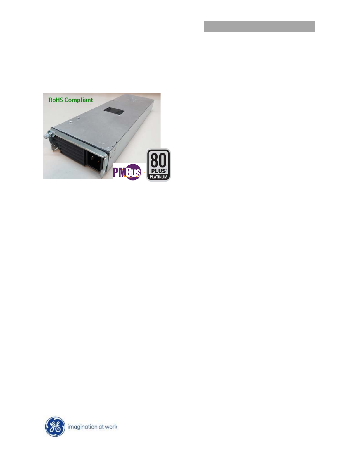
CAR2012TE series rectifier
Input: 85Vac to 264Vac; Output: 12Vdc @ 2000W; 3.3 @ 4A or 5Vdc @ 3A Standby
Features
Efficiency: 95 % @ 50% load. Under most load conditions
exceeding 80plus “Titanium” criteria
Universal input with PFC
Constant power characteristic
2 front panel LEDs: 1-input;2-[DC_OK, fault, warning]
Remote ON/OFF control of the 12Vdc output
Remote sense on the 12Vdc output
No minimum load requirements
Active load sharing (single wire)
Hot Plug-ability
Standby orderable either as 3.3Vdc @ 4A or 5Vdc @ 3A
Auto recoverable OC & OT protection
Operating temperature: -10 - 70C (de-rated above 50C)
Digital status & control: PMBus serial bus
EN/IEC/UL/CSA C22.2 60950-1 2
CE mark§
Meets FCC part 15, EN55022 Class A standards
Meets EN61000 immunity and transient standards
Shock & vibration: Meets IPC 9592 Class II standards
nd
Applications
12Vdc distributed power architectures
Datacom and Telecom applications
Mid to high-end Servers
Routers/Switches
Broadband Switches
ATE Equipment
edition +A1, CCC
Description
The CAR2012TE Front-End provides highly efficient isolated power from worldwide input mains in a compact 1U
industry standard form factor. This power supply is ideal for applications where mid to light load efficiency is of key
importance in order to reduce system power consumption during ‘typical’ operational conditions.
The high-density, front-to-back airflow is designed for minimal space utilization and is highly expandable for future
growth. The industry standard PMBus compliant I
monitoring capabilities. The SMBAlert signal pin automatically alerts customers of any state change within the power
supply.
*
UL is a registered trademark of Underwriters Laboratories, Inc.
† CSA is a registered trademark of Canadian Standards Association.
‡ VDE is a trademark of Verband Deutscher Elektrotechniker e.V.
§ Intended for integration into end-user equipment. All the required procedures for CE marking of end-user equipment should be followed. (The CE mark is placed on selected products.)
** ISO is a registered trademark of the International Organization of Standards.
+ PMBus name and logo are registered trademarks of the System Management Interface Forum (SMIF)
February 9, 2014 ©2013 General Electric Company. All rights reserved.
2
C communications buss offers a full range of control and
Page 2
GE
Data Sheet
CAR2012TE series rectifier
Input: 85Vac to 264Vac; Output: 12 Vdc @ 2000W; 3.3Vdc or 5 Vdc @ 4A
Absolute Maximum Ratings
Stresses in excess of the absolute maximum ratings can cause permanent damage to the device. These are absolute stress ratings only, functional
operation of the device is not implied at these or any other conditions in excess of those given in the operations sections of the data sheet. Exposure
to absolute maximum ratings for extended periods can adversely affect the device reliability.
Parameter Symbol Min Max Unit
Input Voltage: Continuous VIN 0 264 VAC
Operating Ambient Temperature TA -10 70 °C
Storage Temperature Tstg -40 85 °C
I/O Isolation voltage to Frame (100% factory Hi-Pot tested) 2121 VDC
Electrical Specifications
Unless otherwise indicated, specifications apply over all operating input voltage, load, and temperature conditions.
INPUT
Parameter Symbol Min Typ Max Unit
Operational Range VIN 85 115/230 264 VAC
F
Frequency Range (ETSI 300-132-1 recommendation)
IN
Main Output Turn OFF
V
IN
Hysteresis between turn OFF and turn ON 3 5
Maximum Input Current (VO= V
VIN= 180VAC
Cold Start Inrush Current (Excluding x-caps, 25C, <10ms,
per ETSI 300-132)
Efficiency (T
=25C, VO= 12V) VIN
amb
O, set
, IO=I
) VIN= 100VAC
O, max
I
IN
I
IN
100% load
50% load
20% load
10% load
Power Factor (VIN=115/230VAC), IO= 50% I
IO= I
O, max
Holdup time (Vout = 12.0VDC, Tamb 25C, IO=80% I
V
= 230VAC
in
= 100VAC
V
IN
Early warning prior to output falling below regulation1
(Vout = 12.0V
, Tamb 25C, IO=80% I
DC
O, max
O, max
)
O, max
PF
)
T 12
2
Ride through T 10
Leakage Current (VIN= 250VAC, FIN = 60Hz) I
Isolation Input/Output
IN
Input/Frame 2121 V
Output/Frame 100 V
12Vdc MAIN OUTPUT
Parameter Symbol Min Typ Max Unit
Output Power 180 – 264 / 90-132 Vac
V
≤ 90V
AC
AC
Set point
Overall regulation (load, temperature) -2 +2 %
W
V
O
47 50/60 63 Hz
75 82
VAC Main Output Turn ON 80 88
40 A
15.5
12.5
AAC
PEAK
115V / 230V
92 / 93.0
93 / 95.0
%
91 / 94.0
85 / 91.0
0.98
0.99
20
3 mA
3000 V
0 - 2000/1300 W
0 - 1200 W
11.9 12.00 12.1 V
ms
RMS
AC
DC
DC
DC
1
Measured by the DC_OK signal going LO prior to the output decaying below 10.8Vdc
February 9, 2014 ©2013 General Electric Company. All rights reserved. Page 2
Page 3
GE
Data Sheet
CAR2012TE series rectifier
Input: 85Vac to 264Vac; Output: 12 Vdc @ 2000W; 3.3Vdc or 5 Vdc @ 4A
MAIN OUTPUT (continued)
12V
dc
Parameter Symbol Min Typ Max Unit
Ripple and noise2 at 25C, ( relaxed to 150mV
below 0C)
P-P
120
Turn-ON overshoot +3 %
Turn-ON delay T 2 sec
Remote ON/OFF delay time
Turn-ON rise time (10 – 90% of V
)
out
Transient response 50% step [10%-60%, 50% - 100%]
(dI/dt – 1A/µs, recovery 300µs)
Programmable range (hardware & software) 10.8 13.2
V
O
Overvoltage protection, latched
(recovery by cycling OFF/ON via hardware or software)
Output current 180 ≥ VIN ≥ 264
90 ≥ V
Current limit, Hiccup (programmable level) 110 130 % of FL
Active current share, ( IO ≥ 20% of I
≥ 132
IN
I
O
) -5 +5 % of FL
O,MAX
40 ms
50 ms
-5 +5 %V
13.8 14.8 15.8
0
167
108
STANDBY OUTPUT
Parameter Symbol Min Typ Max Unit
Set point VO 3.3 / 5.0 V
Overall regulation (load, temperature, aging) VO -5 +5 %
Ripple and noise, STANDBY
CLOCK – I
DATA – I
2
C
2
C
Output current [3.3V / 5V] I
O
0 4 / 3 A
100 mV
Overload protection - 110 150 % of FL
Isolation Output/Frame 100
mV
P-P
O
V
DC
V
DC
A
DC
DC
P-P
DC
V
DC
General Specifications
Parameter Min Typ Max Units Notes
Reliability, 25C
50C
320,000
100,000
Hrs
Service Life 10 Yrs Full load, excluding fans
Weight
Full load, ; MTBF per SR232 Reliability protection for
electronic equipment, method I, case III,
Feature Specifications
Unless otherwise indicated, specifications apply over all operating input voltage, resistive load, and temperature conditions. See
Feature Descriptions for additional information.
Parameter Symbol Min Typ Max Unit
Remote ON/OFF (pulled up internally within the module)
Logic High (Module ON)
Logic Low (Module OFF) I
V
2
Measured across a 10µf tantalum and a 0.1µf ceramic capacitors in parallel. 20MHz bandwidth
0.7V
IL
IL
V
STDBY
0
V
STDBY
DC
1 mA
0.8 VDC
February 9, 2014 ©2013 General Electric Company. All rights reserved. Page 3
Page 4

GE
Data Sheet
CAR2012TE series rectifier
Input: 85Vac to 264Vac; Output: 12 Vdc @ 2000W; 3.3Vdc or 5 Vdc @ 4A
Feature Specifications (continued)
Parameter Symbol Min Typ Max Unit
Output Voltage programming (Vprog)
Equation: Vout = 10.8 + (Vprog * 0.96)
Vprog range V
Programmed output voltage range Vo
Voltage adjustment resolution (8-bit A/D) Vo
Output configured to 13.2Vdc V
Output configured to the 12Vdc set-point V
Interlock [short pin controlling presence of the 12VDC output]
12V output OFF VI
12V output ON VI
AC-OK (internally pulled up to Stndby via a 10kΩ resistor)
Logic High (Input within normal range) I
V
Logic Low (Input out of range) I
V
DC-OK (internally pulled up to Stndby via a 10kΩ resistor)
Logic High (Output voltage is present; V
≥ 10.7Vdc) I
OUT
V
Logic Low (Output voltage is not present; V
≤ 10.2V
OUT
) I
DC
V
prog
0
10.8
2.5 3.0 VDC
prog
prog
3.0
10
2.5 VDC
13.2 VDC
mVDC
VDC
0.7V
DD
0
12 V
0.8 VDC
DC
OH
OL
OH
OL
0.7V
DD
0
20 µA
12 V
DC
4 mA
0.4 VDC
OH
OL
OH
OL
0.7V
DD
0
20 µA
12 V
DC
4 mA
0.4 VDC
OT Warning (internally pulled up to Stndby via a 10kΩ resistor)
Logic High (temperature within normal range) I
V
Logic Low (temperature is too high) I
V
OH
OL
OH
OL
0.7V
DD
0
20 µA
12 V
DC
4 mA
0.4 VDC
Delayed shutdown after Logic Low transition Tdelay 10 sec
Fault (internally pulled up to Stndby via a 10kΩ resistor)
Logic High (No fault is present) I
V
Logic Low (Fault is present) I
V
PS Present (connected to output GRD inside the power supply)
Logic High (Power supply is not plugged in)
Logic Low (Power supply is present) VIL 0
OH
OL
OH
OL
0.7V
DD
0
20 µA
12 V
DC
4 mA
0.4 VDC
0.1 VDC
February 9, 2014 ©2013 General Electric Company. All rights reserved. Page 4
Page 5
GE
Data Sheet
CAR2012TE series rectifier
Input: 85Vac to 264Vac; Output: 12 Vdc @ 2000W; 3.3Vdc or 5 Vdc @ 4A
Feature Specifications (continued)
Parameter Symbol Min Typ Max Unit
SMBAlert# (Interrupt) (must be pulled up externally to Stndby)
Logic High (No Alert - normal) I
V
Logic Low (Alert is set) I
V
Output current monitor (Imon)
Resolution
Measurement range IO 0 167 ADC
Measurement accuracy, load > 25% of FL, VO = 12VDC -4 +4 %
Analog output range V
Sourced output current IO 5 mADC
Digital Interface Specifications
Parameter Conditions Symbol Min Typ Max Unit
PMBus Signal Interface Characteristics
Input Logic High Voltage (CLK, DATA) VIH 0.7V
Input Logic Low Voltage (CLK, DATA) VIL 0 0.8 V
Input high sourced current (CLK, DATA) IIH 0 10 μA
Output Low sink Voltage (CLK, DATA, SMBALERT#) IO=5mA VOL 0.4 V
Output Low sink current (CLK, DATA, SMBALERT#) IOL 5 mA
Output High open drain leakage current (CLK,DATA,
SMBALERT#)
PMBus Operating frequency range FPMB 10 400 kHz
Measurement System Characteristics
Clock stretching tSTRETCH 25 ms
I
measurement range
OUT
I
measurement accuracy 25°C
OUT
V
measurement range
OUT
V
measurement accuracy
OUT
Temp measurement range
Temp measurement accuracy3
IIN measurement range Linear mode
IIN measurement accuracy
VIN measurement range
VIN measurement accuracy
PIN measurement range
PIN measurement accuracy
Fan Speed measurement range
Fan Speed measurement accuracy
Fan speed control range
V
=3.6V I
O
Linear mode
Linear mode
Linear mode
Linear mode
Linear mode
Linear mode
Linear mode
OH
OH
OL
0
OL
0.7V
DD
20 µA
12 V
DC
4 mA
0.4 VDC
0 3.3 VDC
mon
OH
I
RNG
I
ACC
V
OUT(rng)
V
OUT(acc)
Temp
Temp
I
IN(rng)
I
IN(acc)
V
IN(rng)
V
IN(acc)
P
N(rng)
P
IN(acc)
18 mV/A
3.6 V
(rng)
(acc)
DD
0 10 μA
0 167 A
-5 +5 %
0 14 V
-5 +5 %
0 125
-5 +5 %
0 18 A
-5 +5 %
0 300 V
-5 +5 %
0 3000 W
-5 +5 %
0 30k RPM
-10 10 %
0 100 %
C
rms
rms
3
Temperature accuracy reduces non-linearly with decreasing temperature
February 9, 2014 ©2013 General Electric Company. All rights reserved. Page 5
Page 6
GE
Data Sheet
CAR2012TE series rectifier
Input: 85Vac to 264Vac; Output: 12 Vdc @ 2000W; 3.3Vdc or 5 Vdc @ 4A
Environmental Specifications
Parameter Min Typ Max Units Notes
Ambient Temperature
Storage Temperature -40 85 °C
Operating Altitude 2250/7382 m/ft
Non-operating Altitude 8200/30k m / ft
Power Derating with Temperature 2.5
Power Derating with Altitude 2.0
Acoustic noise 55
Over Temperature Protection 125/110 °C Shutdown / restart
Humidity
Operating
Storage
Shock and Vibration Meet IPC 9592 Class II, Section 5 requirements
EMC Compliance
-10 70 °C
%/°C
C/301 m
Derated above 50C
50C to 70C
Above 2250 m/7382 ft
C/1000 ft
30
10
45
95
dbA
% Relative humidity, non-condensing
95
Full load
Half load
Parameter Function Standard Level Criteria Test
Conducted
AC input
AC input
immunity
Enclosure
immunity
* Note: Contact the factory for a recommended external EMI filter to meet Class B emissions
**
Radiated emissions compliance is contingent upon the final system configuration.
Criteria Performance
A No performance degradation
B Temporary loss of function or degradation not requiring manual intervention
C Temporary loss of function or degradation that may require manual intervention
D Loss of function with possible permanent damage
emissions
Radiated
emissions**
Voltage dips EN61000-4-11 A -30%, 10ms
Voltage surge EN61000-4-5 A 4kV, 1.2/50µs, common mode
Fast transients EN61000-4-4 A 5/50ns, 2kV (common mode)
Conducted RF
fields
Radiated RF fields EN61000-4-3 A 10V/m, 80-1000MHz, 80% AM
ESD EN61000-4-2 B 4kV contact, 8kV air
EN55022, FCC part 15
EN61000-3-2
EN55022 A* 30 – 10000MHz
EN61000-4-6 A 130dBµV, 0.15-80MHz, 80% AM
ENV 50140 A
A* 0.15 – 30MHz
0 – 2 KHz
B -60%, 100ms
B -100%, 5sec
A 2kV, 1.2/50µs, differential mode
February 9, 2014 ©2013 General Electric Company. All rights reserved. Page 6
Page 7

00 0 0
GE
Data Sheet
CAR2012TE series rectifier
Input: 85Vac to 264Vac; Output: 12 Vdc @ 2000W; 3.3Vdc or 5 Vdc @ 4A
Control and Status
Control hierarchy: Some features, such as output voltage,
can be controlled both through hardware and firmware. For
example, the output voltage is controlled both by a signal pin
(Vprog) and a PMBus command, (OPERATION) .
Unless otherwise noted, the signal pin controls the feature
until the firmware command is executed. However, once the
firmware command has been executed, the signal pin is
ignored. In the above example, the power supply will no
longer ‘listen’ to the Vprog pin if the OPERATION command
has been executed.
In summary, Vprog is utilized for initialized configuration of
the output voltage and to change the output voltage when
PMBus is not used for that function.
Analog controls: Details of analog controls are provided in
this data sheet under Signal Definitions.
Common ground: All signals and outputs are referenced to
Output return. These include ‘Vstb return’ and ‘Signal return’.
Delayed overcurrent shutdown during startup: Power
supplies are programmed to stay in a constant current state
for up to 20 seconds during power up. This delay has been
introduced to permit the orderly application of input power to
a subset of paralleled front-ends during power up. If the
overload persists beyond the 20 second delay, the front-end
will revert back into its programmed state of overload
protection.
Unit in Power Limit or in Current Limit: When output
voltage is > 10V
When output voltage is < 10VDC, if the unit is in the RESTART
mode, it goes into hiccup. When the unit is ON the output LED
is ON, when the unit is OFF the output LED is OFF.
When the unit is in latched shutdown the output LED is
Auto_restart: Auto-restart is the default configuration for
over-current and over-temperature shutdowns. These
features are configured by the PMBus™ fault_response
commands
An overvoltage shutdown is followed by three attempted
restarts, each restart delayed 1 second, within a 1 minute
window. If within the 1 minute window three attempted
restarts failed, the unit will latch OFF. If within the 1 minute
less than 3 shutdowns occurred then the count for latch OFF
resets and the 1 minute window starts all over again.
Restart after a latchoff: PMBus™ fault_response commands
can be configured to direct the power supply to remain
latched off for over_temperature and over_current.
To restart after a latch off either of five restart mechanisms
are available.
1. The hardware pin Remote ON/OFF may be cycled
the Output LED will continue blinking.
DC
OFF and then ON.
OFF.
2. The unit may be commanded to restart via i2c
through the Operation command by cycling the
output OFF followed by ON.
3. Remove and reinsert the unit.
4. Turn OFF and then turn ON AC power to the unit.
5. Changing firmware from latch off to restart.
Each of these commands must keep the power supply in the
OFF state for at least 2 seconds, with the exception of
changing to restart.
A successful restart shall clear all alarm registers, set the
restarted successful bit of the Status_2 register.
A power system that is comprised of a number of power
supplies could have difficulty restarting after a shutdown
event because of the non-synchronized behavior of the
individual power supplies. Implementing the latch-off
mechanism permits a synchronized restart that guarantees
the simultaneous restart of the entire system.
A synchronous restart can be implemented by;
1. Issuing a GLOBAL OFF and then ON command to all power
supplies,
2. Toggling Off and then ON the ENABLE signal
3. Removing and reapplying input commercial power to the
entire system.
The power supplies should be turned OFF for at least 20 – 30
seconds in order to discharge all internal bias supplies and
reset the soft start circuitry of the individual power supplies.
Control Signals
MCU Device address: Address bits A2, A1, A0 configure the
specific address of the power supply. With these four bits, up
to sixteen (8) modules to be addressed on a single I²C bus.
The pins are pulled HI internal to the power supply. For a logic
LO these pins should be connected to ‘Output Return’. The
least significant bit x (LSB) of the address byte is set to either
write [0] or read [1]. A write command instructs the power
supply. A read command accesses information from the
power supply.
Device
MCU Cx 1 1 0 0 A2 A1 A0 R/W
Broadcast
Global Broadcast: This is a powerful command because it
instruct all power supplies to respond simultaneously.. A read
instruction should never be accessed globally. The power
supply should issue a ‘invalid command’ state if a ‘read’ is
attempted globally.
For example, changing the ‘system’ output voltage requires
this capability so that all paralleled power supplies change
their output simultaneously. This command can also turn OFF
the ‘main’ output or turn ON the ‘main’ output of all power
supplies simultaneously. Unfortunately, this command does
have a side effect. Only a single power supply needs to pull
down the ninth acknowledge bit. To be certain that each
power supply responded to the global instruction, a READ
Address
Address Bit Assignments
(Most to Least Significant)
0 0 0 0 0 0
February 9, 2014 ©2013 General Electric Company. All rights reserved. Page 7
Page 8

GE
Data Sheet
CAR2012TE series rectifier
Input: 85Vac to 264Vac; Output: 12 Vdc @ 2000W; 3.3Vdc or 5 Vdc @ 4A
instruction should be executed to each power supply to verify
that the command properly executed.
Voltage programming (V
signal can vary the output voltage ± 10% from 10.8Vdc to
13.2Vdc.
Hardware voltage programming controls the output voltage
until a software margin command is executed. Software
voltage programming (margining) permanently overrides the
hardware margin setting and the power supply no longer
listens to any hardware margin settings until power to the
controller is interrupted, for example if input power or bias
power is recycled.
When bias power is recycled to the controller the controller
restarts into its default configuration, programmed to set the
output as instructed by the V
software commanded settings permanently override the
margin setting. As an example, adding a resistor between
and Output_return is an effective way of changing the
V
prog
factory set point of the rectifier to whatever voltage level is
desired by the user during initial start-up.
Load share (I
generated and acted upon automatically by power supplies
connected in parallel. I
other for power supplies, if active current share among the
power supplies is desired. No resistors or capacitors should
get connected to this pin.
Remote ON/OFF: Controls the presence of the main 12Vdc
output voltage. This is an open collector signal that needs to
be pulled HI externally through a resistor.
A turn OFF command either through this signal (Remote
ON/OFF) or firmware commanded would turn OFF the 12V
output.
Interlock: This is a short signal pin that controls the presence
of the 12Vdc main output. This pin should be connected to
‘output return’ on the system side of the output connector.
The purpose of this pin is to ensure that the output turns ON
after engagement of the power blades and turns OFF prior to
disengagement of the power blades.
): This is a single wire analog signal that is
share
): An analog voltage on this
prog
pin. Again, subsequent
prog
pins should be connected to each
share
Over temp warning: A TTL compatible status signal
representing whether an over temperature exists. This signal
needs to be pulled HI externally through a resistor.
If an over temperature should occur, this signal would pull LO
for approximately 10 seconds prior to shutting down the
power supply. In its default configuration, the unit would
restart if internal temperatures recover within normal
operational levels. At that time the signal reverts back to its
open collector (HI) state.
Fault: A TTL compatible status signal representing whether a
Fault occurred.
This signal activates for internal power supply failures such as
over temperature or over voltage shutdown.
PS Present: This pin is connected to ‘output return’ within the
power supply. Its intent is to indicate to the system that a
power supply is present.
Serial Bus Communications
The I²C interface facilitates the monitoring and control of
various operating parameters within the unit and transmits
these on demand over an industry standard I²C Serial bus.
All signals are referenced to ‘Signal Return’.
Pull-up resistors: The clock, data, and SMBusAlert# lines do
not have any internal pull-up resistors inside the power
supply. The customer is responsible for ensuring that the
transmission impedance of the communications lines
complies with I
Serial Clock (SCL): The clock pulses on this line are generated
by the host that initiates communications across the I²C
Serial bus. This signal needs to be pulled HI externally through
a resistor as necessary to ensure that rise and fall time timing
and the maximum sink current is in compliance to the I²C
/SMBus specifications.
Serial Data (SDA): This line is a bi-directional data line. This
signal needs to be pulled HI externally through a resistor as
necessary to ensure that rise and fall time timing and the
maximum sink current is in compliance to the I²C /SMBus
specifications.
2
C and SMBus standards.
Status signals
Output current monitor (Imon): A voltage level of 3V = 167A,
or 18mV/A, proportional to the delivered output current is
present on this pin.
AC OK: A TTL compatible status signal representing whether
the input voltage is within the anticipated range. This signal
needs to be pulled HI externally through a resistor.
DC OK: A TTL compatible status signal representing whether
the output voltage is present. This signal needs to be pulled HI
externally through a resistor.
February 9, 2014 ©2013 General Electric Company. All rights reserved. Page 8
SMBUSAlert#: This hardware signal pin is normally HI. When
asserted (logic LO) it signifies to the system controller that the
state of the power supply has changed or that
communication errors occurred.
Basic Operation
PMBus™ compliance: The power supply is fully compliant to
the Power Management Bus (PMBus™) rev1.2 requirements.
The power supply clears the STATUS and ALARM registers and
the SMBAlert# signal after a successful read back of the
information in these registers, with the exception of
communications error alarms (PEC error, data error,
command error). If the alarm state is still present the status
Page 9

GE
Data Sheet
CAR2012TE series rectifier
Input: 85Vac to 264Vac; Output: 12 Vdc @ 2000W; 3.3Vdc or 5 Vdc @ 4A
and alarm registers get reset into their alarm state, however,
the SMBAlert# does not assert again.
‘Manufacturer Specific’ commands are used to support
instructions that are not offered by the PMBus™ specification.
All communication over the PMBus interface must support
Packet Error Checking (PEC). The PMBus master must
generate the correct PEC byte for all transactions, and check
the PEC byte returned by the power supply.
Non-volatile memory is used to store configuration settings.
Not all settings programmed into the device are
automatically saved into this non-volatile memory. Only those
specifically identified as capable of being stored can be
saved. (see the Table of Commands for which command
parameters can be saved to non-volatile storage).
Default state:
state to automatically restart after a shutdown has occurred
for over current and over temperature. The default state can
be reconfigured by changing non-volatile memory
(Store_default_code).
Re-initialization: The I2C code is programmed to re-initialize if
no activity is detected on the bus for 5 seconds. Reinitialization is designed to guarantee that the I
does not hang up the bus. Although this rate is longer than
the timing requirements specified in the SMBus specification,
it had to be extended in order to ensure that a re-initialization
would not occur under normal transmission rates. During the
few µseconds required to accomplish re-initialization the I
µController may not recognize a command sent to it. (i.e. a
start condition).
Read back delay: The power supply issues the SMBAlert #
notification as soon as the first state change occurred. During
an event a number of different states can be transitioned to
before the final event occurs. If a read back is implemented
rapidly by the host a successive SMBAlert# could be triggered
by the transitioning state of the power supply. In order to
avoid successive SMBAlert# s and read back and also to
avoid reading a transitioning state, it is prudent to wait more
than 2 seconds after the receipt of an SMBAlert# before
executing a read back. This delay will ensure that only the
final state of the power supply is captured.
Successive read backs: Successive read backs to the power
supply should not be attempted at intervals faster than every
one second. This time interval is sufficient for the internal
processors to update their data base so that successive
reads provide fresh data.
Non-supported commands: Non supported commands are
flagged by setting the appropriate STATUS bit and issuing an
SMBAlert# to the ‘host’ controller. If a non-supported read is
requested the power supply will return 0x00h for data.
Data out-of-range: The power supply validates data settings
and sets the data out-of-range bit and SMBAlert# if the data
is not within acceptable range.
Master/Slave: The ‘host controller’ is always the MASTER.
Power supplies are always SLAVES. SLAVES cannot initiate
Power supplies are programmed in the default
2
C µController
2
C
communications or toggle the Clock. SLAVES also must
respond expeditiously at the command of the MASTER as
required by the clock pulses generated by the MASTER.
Clock stretching: The ‘slave’ µController inside the power
supply may initiate clock stretching if it is busy and it desires
to delay the initiation of any further communications. During
the clock stretch the ‘slave’ may keep the clock LO until it is
ready to receive further instructions from the host controller.
The maximum clock stretch interval is 25ms.
The host controller needs to recognize this clock stretching,
and refrain from issuing the next clock signal, until the clock
line is released, or it needs to delay the next clock pulse
beyond the clock stretch interval of the power supply.
Note that clock stretching can only be performed after
completion of transmission of the 9
being the START command.
Figure 1. Example waveforms showing clock stretching.
I²C Bus Lock-Up detection: The device will abort any
transaction and drop off the bus if it detects the bus being
held low for more than 35ms.
Communications speed: Both 100kHz and 400kHz clock
rates are supported. The power supplies default to the
100kHz clock rate. The minimum clock speed specified by
SMBus is 10 kHz.
Packet Error Checking (PEC): The power supply will not
respond to commands without the trailing PEC because the
integrity of communications is compromised without packet
error correction deployment.
PEC is a CRC-8 error-checking byte, based on the polynomial
8
+ x2 + x + 1, in compliance with PMBus™
C(x) = x
requirements. The calculation is performed on all message
bytes, including the originating write address and command
bytes preceding read instructions. The PEC is appended to the
message by the device that supplied the last byte.
SMBAlert#: The µC driven SMBAlert# signal informs the
‘master/host’ controller that either a STATE or ALARM change
has occurred. Normally this signal is HI. The signal will change
to its LO level if the power supply has changed states and the
signal will be latched LO until the power supply receives a
‘clear’ instruction as outlined below. If the alarm state is still
present after the ‘clear_faults’ command has been received,
then the signal will revert back into its LO state again and will
latch until a subsequent ‘clear_faults’ signal is received from
the host controller.
th
ACK bit, the exception
Clock
Stretch
February 9, 2014 ©2013 General Electric Company. All rights reserved. Page 9
Page 10

GE
Data Sheet
CAR2012TE series rectifier
Input: 85Vac to 264Vac; Output: 12 Vdc @ 2000W; 3.3Vdc or 5 Vdc @ 4A
The signal will be triggered for any state change whether a
‘warning’ or a ‘fault’, including the following conditions;
VIN under or over voltage
Vout under or over voltage
IOUT over current
Over Temperature
Fan Failure
Communication error
PEC error
Invalid command
Detected internal faults
The power supply will clear the SMBusAlert# signal (release
the signal to its HI state) upon the following events:
Receiving a CLEAR_FAULTS command
Input power and bias power to the processor is recycled
The power supply will clear the SMBusAlert# signal (release
the signal to its HI state) for operational alarms (but not
communications alarms that require a clear_faults signal
from the controller that it received the alert) upon the
following events:
The main output recycled (turned OFF and then ON) via
the Remote_ON/OFF or INTERLOCK signal pins
The main output recycled (turned OFF and then ON) by
the OPERATION command
Standard instruction:
Up to two bytes of data may follow an
instruction depending on the required data content. Analog
data is always transmitted as LSB followed by MSB. PEC is
optional and includes the address and data fields.
1 8 1 8 1
S Slave address Wr A Command Code A
Master to Slave Slave to Master
SMBUS annotations; S – Start , Wr – Write, Sr – re-Start, Rd
– Read,
A – Acknowledge, NA – not-acknowledged, P – Stop
Standard READ:
request depending on the required data content. Analog
data is always transmitted as LSB followed by MSB. PEC is
mandatory and includes the address and data fields
8 1 8 1 8 1 1
Low data byte A High data byte A PEC A P
Up to two bytes of data may follow a READ
.
1 7 1 1 8 1
S Slave address Wr A Command Code A
1 7 1 1 8 1
Sr Slave Address Rd A LSB A
8 1 8 1 1
MSB A PEC No-ack P
Block communications: When writing or reading more than
two bytes of data at a time BLOCK instructions for WRITE and
READ commands are used instead of the Standard
Instructions above to write or read any number of bytes
greater than two.
Block write format:
1
S Slave address Wr A Command Code A
Byte count = N A Data 1 A Data 2 A
7 1 1 8 1
8 1 8 1 8 1
8 1 8 1 8 1 1
………. A Data N ≤ 48 A PEC A P
Block read format:
1
S Slave address Wr A Command Code A
7 1 1 8 1
1 7 1 1
Sr Slave Address Rd A
8 1 8 1 8 1
Byte count = N A Data 1 A Data 2 A
8 1 8 1 8 1 1
………. A Data N ≤ 48 A PEC NoAck P
An example of the block_read instruction is the
Read_std_parameters (D0h) command. This ‘manufacturer
specific’ command returns STATUS and ALARM register data,
output voltage, output current, and internal temperature in a
single read string.
1 8 1
S Slave address Wr A Command Code A
1 8 1 8 1
Sr Slave address Rd A Byte count = 11 A
8 1 8 1 8 1
Status-2 A Status-1 A Alarm-2 A
8 1 8 1 8 1
Alarm-1 A Voltage LSB A Voltage MSB A
8 1 8 1
Current LSB A Current MSB A
8 1 8 1 8 1 1
Temperature LSB A Temperature MSB A PEC NA P
Linear Data Format The definition is identical to Part II of the
PMBus Specification. All standard PMBus values, with the
exception of output voltage related functions, are
represented by the linear format described below Output
voltage functions are represented by a 16 bit mantissa. The
value of the exponent for output voltage functions is listed in
the Vout_mode command.
8 1
February 9, 2014 ©2013 General Electric Company. All rights reserved. Page 10
Page 11

GE
CAR2012TE series rectifier
Input: 85Vac to 264Vac; Output: 12 Vdc @ 2000W; 3.3Vdc or 5 Vdc @ 4A
The Linear Data Format is a two byte value with an 11-bit,
two’s complement mantissa and a 5-bit, two’s complement
exponent or scaling factor, its format is shown below.
Data Byte High Data Byte Low
Bit 7 6 5 4 3 2 1 0 7 6 5 4 3 2 1 0
Exponent (E) Mantissa (M)
The relationship between the Mantissa, Exponent, and Actual
Value (V) is given by the following equation:
E
MV 2
Where:
V is the value
M is the 11-bit, two’s complement mantissa
E is the 5-bit, two’s complement exponent
Standard features
Command Comments
ON_OFF_CONFIG Both the CNTL pin, enabling or disabling
Vout_OV_fault_response Only latched (0x80) is supported
CAPABILITY 400KHz, SMBALERT
PMBus revision 1.2
the output, and the OPERATION command
are supported. Other options are not
supported.
PMBusTM Command set:
Non-supported commands are annunciated.
Command
Operation 0x01 1 Output ON/OFF
ON_OFF_config 0x02 1 09, output ON default
Clear_faults 0x03 0 Clear Status
Write_protect 0x10 1 Write control
Restore_default_all 0x12 0 Reset defaults
Store_default_code 0x13 1 Change default state
Vout_mode 0x20 1 Vout constants
Vout_command 0x21 2 Set Vout
Fan_command_1 0x3B 2 Set fan speed in %
Vout_OV_fault_limit 0x40 2 Set OV fault limit
Vout_OV_warn_limit 0x42 2 Set OV warn limit
Iout_OC_fault_limit 0x46 2
Iout_OC_fault_response4
Iout_OC_warn_limit 0x4A 2
OT_fault_limit 0x4F 2
OT_fault_response5 0x50 1
OT_warn_limit 0x51 2
Status_byte 0x78 1
Status_word 0x79 2
Status_Vout 0x7A 1
Status_Iout 0x7B 1
Status_input 0x7C 1
Status_temperature 0x7D 1
Status_CML 0x7E 1
Status_fan_1_2 0x81 1
Read_Iin 0x89 2
4
Only latched (0xC0) or hiccup (0xF8) are supported
5
Only latched (0x80) or restart (0xC0) are supported
Hex
Data
Code
Byte Function
0x47 1
Latch or hiccup
Set OC warn limit
Latch or hiccup
Set OT warn limit
Command
Read_Vout 0x8B 2
Read_Iout 0x8C 2
Read_temperature 0x8D 2
Read_fan_speed_1 0x90 2
Read_fan_speed_2 0x91 2
Read_Pin 0x97 2
Mfr_ID 0x99 5
Mfr_model 0x9A 16
Mfr_serial 0x9E 15
Read_Std_Parameters 0xD0 10
Read_Status_State 0xD1 2
Read_Alarm_State 0xD2 2
Read_fan_speed 0xD3 4
Read_Input_string 0xD4 2
Read_mfr_rev 0xD5 4
Read_Run_Timer 0xD6 3
EEPROM_record 0xD9 64
Test Function 0xDF 1
Code
Command Descriptions
Operation (0x01) : By default the Power supply is turned ON
at power up as long as Power ON/OFF signal pin is active HI.
The Operation command is used to turn the Power Supply ON
or OFF via the PMBus. The data byte below follows the
OPERATION command.
FUNCTION
Unit ON 80
Unit OFF 00
To RESET the power supply cycle the power supply OFF, wait
at least 2 seconds, and then turn back ON. All alarms and
shutdowns are cleared during a restart.
Clear_faults (0x03): This command clears all STATUS and
FAULT registers and resets the SMBAlert# line.
If a fault still persists after the issuance of the clear_faults
command the specific registers indicating the fault are reset
and the SMBAlert# line is activated again.
WRITE_PROTECT register (0x10): Used to control writing to
the PMBus device. The intent of this command is to provide
protection against accidental changes. All supported
command parameters may have their parameters read,
regardless of the write_protect settings. The default setting of
this register is disable_all_writes except write_protect 0x80h.
Enable all writes 00
Disable all writes except write_protect 80
Disable all writes except write_protect and
OPERATION
Restore_Default_All (0x12): Restores all register values and
responses to the default parameters set in the power supply.
DATA BYTE
FUNCTION
Data Sheet
Hex
Data
Byte Function
CAR2012TEXXXZ01A
01KZ51018193xxx
DATA BYTE
40
February 9, 2014 ©2013 General Electric Company. All rights reserved. Page 11
Page 12

GE
Data Sheet
CAR2012TE series rectifier
Input: 85Vac to 264Vac; Output: 12 Vdc @ 2000W; 3.3Vdc or 5 Vdc @ 4A
Store_default_code (0x13): Default values desired to be
overwritten must be executed one at a time. In this fashion
some protection is offered to ensure that only those values
that are desired to be changed are in fact changed.
Vout_mode (0x20): This is a ‘read only’ register. The upper
three bits specify the supported data format, in this case
Linear mode. The lower five bits specify the exponent of the
data being read back in two’s complement binary format for
output voltage related commands, such as Vout_command.
These commands have a 16 bit mantissa. The exponent is
fixed by the module and is returned by this command.
Mode Bits [7:5] Bits [4:0] (exponent)
Linear 000b xxxxxb
Vout_Command (0x21) : This command is used to change the
output voltage of the power supply.
Changing the output voltage should be performed
simultaneously to all power supplies operating in parallel
using the Global Address (Broadcast) feature. If only a single
power supply is instructed to change its output, it may
attempt to source all the required power which can cause
either a power limit or shutdown condition.
Software programming of output voltage permanently
overrides the set point voltage configured by the Vprog
signal pin. The program no longer looks at the ‘Vprog pin’ and
will not respond to any hardware voltage settings. If power is
removed from the µController it will reset itself into its default
configuration looking at the Vprog signal for output voltage
control. In many applications, the Vprog pin is used for
setting initial conditions, if different that the factory setting.
Software programming then takes over once I
communications are established.
To properly hot-plug a power supply into a live backplane, the
system generated voltage should get re-configured into
either the factory adjusted firmware level or the voltage level
reconfigured by the margin pin. Otherwise, the voltage state
of the plugged in power supply could be significantly different
than the powered system.
Voltage margin range: 10.8Vdc – 13.2 Vdc.
Fan_command_1 (0x3B): This command instructs the power
supply to increase the speed of the fan. The transmitted data
byte represents the hex equivalent of the duty cycle in
percentage, i.e. 100% = 0 x 64h. The command can only
increase fan speed, it cannot instruct the power supply to
reduce the fan speed below what the power supply requires
for internal control.
Sending 00h tells the power supply to revert back to its
internal control.
Vout_OV_fault_limit (0x40): Sets the value at which the main
output voltage will shut down. The default OV_fault value is
set at 60Vdc. This level can be permanently changed and
stored in non-volatile memory.
2
C
Vout_OV_warn_limit (0x42): OV_warning is extremely useful
because it gives the system controller a heads up that the
output voltage is drifting out of regulation and the power
supply is close to shutting down. Pre-amative action may be
taken before the power supply would shut down and
potentially disable the system. This level can be permanently
changed and stored in non-volatile memory.
Iout_OC_fault_limit (0x46): Sets the value at which the power
supply will shut down. The default OC_fault_limit is 68Adc at
high_line and 30A at low_line. (The value is contingent on
whether the power supply operates in the low_line or
high_line mode). This level can be permanently changed and
stored in non-volatile memory. Which level is changed is
contingent on the input voltage applied to the power supply
at the time the change takes place.
Iout_OC_fault_response (0x47): Sets the response if the
output overload exceeds the OC_Fault_limit value. The
default OC_fault_response is hiccup (0xF8). The only two
allowable states are latched (0xC0) or hiccup. The default
response state can be permanently changed and stored in
non-volatile memory. The response is the same for both
low_line and high_line operations.
Iout_OC_warn_limit (0x4A): Sets the value at which the
power supply issues a warning that the output current is
getting too close to the shutdown level. The default
OC_Warn_limit is set to 64.8A at high_line and 27.8A at
low_line. This level can be permanently changed and stored
in non-volatile memory. Which level is changed is contingent
on the input voltage applied to the power supply at the time
the change takes place.
OT_fault_limit (0x4F ): Sets the temperature value at which
the power supply shuts down. The default OT_fault_limit is
set at TBDC. This level can be permanently changed and
stored in non-volatile memory.
OT_fault_response (0x50): Sets the response if the output
overtemperature exceeds the OT_Fault_limit value. The
default OT_fault_response is hiccup (0xC0). The only two
allowable states are latched (0x80) or hiccup. The default
response state can be permanently changed and stored in
non-volatile memory.
OT_warn_limit (0x51): Sets the value at which the power
supply issues a warning that internal temperatures are
getting too close to the shutdown level. The default
OT_Warn_limit is set to TBDC. This level can be permanently
changed and stored in non-volatile memory.
February 9, 2014 ©2013 General Electric Company. All rights reserved. Page 12
Page 13

GE
Data Sheet
CAR2012TE series rectifier
Input: 85Vac to 264Vac; Output: 12 Vdc @ 2000W; 3.3Vdc or 5 Vdc @ 4A
STATUS_BYTE (0x78) : Returns one byte of information with a
summary of the most critical device faults.
Bit
Position
7 Busy 0
6 OFF 0
5 VOUT Overvoltage 0
4 IOUT Overcurrent 0
3 VIN Undervoltage 0
2 Temperature 0
1 CML (Comm. Memory Fault) 0
0 None of the above 0
STATUS_WORD (0x79): Returns status_byte as the low byte
and the following high_byte.
Bit
Position
7 VOUT fault or warning 0
6 IOUT fault or warning 0
5 INPUT 0
4 MFR SPECIFIC 0
3 nPOWER_GOOD 0
2 FANS 0
1 OTHER 0
0 UNKNOWN 0
STATUS_VOUT (0x7A): Returns one byte of information of
output voltage related faults.
Bit
Position
7 VOUT OV Fault 0
6 VOUT_OV_WARNING 0
5 VOUT_UV_WARNING 0
4 VOUT UV Fault 0
3 - 0 Not supported 0
STATUS_IOUT (0x7B): Returns one byte of information of
output current related faults.
Bit
Position
7 IOUT OC Fault 0
6 Not supported 0
5 IOUT OC Warning 0
4- 0 Not supported 0
STATUS_INPUT (0x7C): Returns one byte of information of
input voltage related faults.
Bit
Position
7 VIN_OV_Fault 0
6 VIN_OV_Warning 0
5 VIN_UV_ Warning 0
4 VIN_UV_Fault 0
3 - 0 Not supported 0
Flag
Flag
Flag
Flag
Flag
Default
Value
Default
Value
Default
Value
Default
Value
Default
Value
STATUS_TEMPERATURE (0x7D): Returns one byte of
information of temperature related faults.
Bit
Position
7 OT Fault 0
6 OT Warning 0
5 - 0 Not supported 0
STATUS_CML (0x7E): Returns one byte of information of
communication related faults.
Bit
Position
7 Invalid/Unsupported Command 0
6 Invalid/Unsupported Data 0
5 Packet Error Check Failed 0
4 - 2 Not supported 0
1 Other Communication Fault 0
0 Not supported 0
STATUS_FAN_1_2 (0x81) : Returns one byte of information
with a summary of the most critical device faults.
Bit
Position
7 Fan 1 Fault 0
6 Fan 2 Fault 0
5 - 4 Not supported 0
3 Fan 1 speed overwritten 0
2 Fan 2 speed overwritten 0
1 - 0 Not supported 0
Flag
Flag
Flag
Read back Descriptions
Single parameter read back: Functions can be read back one
at a time using the read_word_protocol with PEC. A
command is first sent out notifying the slave what function is
to be read back followed by the data transfer.
Analog data is always transmitted LSB followed by MSB. A NA
following the PEC byte signifies that the transmission is
complete and is being terminated by the ‘host’.
1 8 1 8 1
S Slave address Wr A Command Code A
1 8 1
Sr Slave address Rd A
Read_fan_speed 1 & 2 (0x90, 0x91): Reading the fan speed is
in Linear Mode returning the RPM value of the fan.
8 1 8 1 8 1 1
LSB A MSB A PEC NA P
Default
Value
Default
Value
Default
Value
February 9, 2014 ©2013 General Electric Company. All rights reserved. Page 13
Page 14

GE
Data Sheet
CAR2012TE series rectifier
Input: 85Vac to 264Vac; Output: 12 Vdc @ 2000W; 3.3Vdc or 5 Vdc @ 4A
Read_FRU_ID (0x99,0x9A, 0x9E): Returns FRU information
1 8 1 8 1
S Slave address Wr A Command 0x9x A
1 8 1 8 1
Sr Slave address Rd A Byte count = x A
8 1 8 1 8 1 8 1 1
high byte A Byte… A low byte A PEC NA P
Mfr_ID (0x99): Manufacturer in ASCII – 5 characters
maximum,
General Electric – Critical Power represented as: GE-CP
Mfr_MODEL (0x9A): Manufacturer model-number in ASCII –
16 characters, for this unit: CAR2012TEBXXZ01A
Mfr_serial (0x9E): Product serial number includes the
manufacturing date, manufacturing location in up to 15
characters. For example:
13KZ51018193xxx, is decoded as;
13 – year of manufacture, 2013
KZ – manufacturing location, in this case Matamoros
51 – week of manufacture
018193xxx – serial #, mfr choice
note: if the additional xxx space is not utilized then F’s
are filled in, (i.e. 018193FFF), ensuring that the actual serial
number is clearly identified.
TM
Manufacturer-Specific PMBus
Many of the manufacturer-specific commands read back
more than two bytes. If more than two bytes of data are
returned, the standard SMBus
process, the Master issues a Write command followed by the
data transfer from the power supply. The first byte of the
Block Read data field sends back in hex format the number of
data bytes, exclusive of the PEC number, that follows. Analog
data is always transmitted LSB followed by MSB. A No-ack
following the PEC byte signifies that the transmission is
complete and is being terminated by the ‘host’.
Mfr_Specific Status and alarm registers: The content and
partitioning of these registers is significantly different than
the standard register set in the PMBus™ specification. More
information is provided by these registers and they are either
accessed rapidly, at once, using the ‘multi parameter’ read
back scheme of this document, or in batches of two STATUS
and two ALARM registers.
TM
Block read is utilized. In this
Commands
Read_std_parameters (0xD0) : This ‘manufacturer specific’
command is the basic read back returning STATUS and
ALARM register data, output voltage, output current, and
internal temperature data in a single read.
1 8 1 8 1
S Slave address Wr A Command Code A
1 8 1 8 1
Sr Slave address Rd A Byte count = 10 A
8 1 8 1 8 1
Status-2 A Status-1 A Alarm-2 A
8 1 8 1 8 1
Alarm-1 A Voltage LSB A Voltage MSB A
8 1 8 1
Current LSB A Current MSB A
8 1 8 1 8 1 1
Temperature LSB A Temperature MSB A PEC NA P
Read_Status_state (0xD1): This command returns the two
STATUS register values using the standard ‘read’ format.
Status-2
Bit
Position
7 PEC Error 0
6
5 Invalid_Instruction 0
4 Power_Capacity [HL = 1] x
3 Isolation test failed 0
2 Restarted_OK 0
1 Data out_of_range 0
0 Remote ON [logic HI = 1] x
Isolation test failed: The ‘system controller’ has to determine
that sufficient capacity exists in the system to take a power
supply ‘off line’ in order to test its isolation capability. Since
the power supply cannot determine whether sufficient
redundancy is available, the results of this test are provided,
but the ‘internal fault’ flag is not set.
Status-1
Bit
Position
7 X 0
6 Isolation_Test_OK 0
5 Internal_Fault 0
4 Shutdown 0
3 Service LED ON 0
2 External_Fault 0
1 LEDs_Test_ON 0
0 Output ON x
Flag
Will restart 0
Flag
Default
Value
Default
Value
February 9, 2014 ©2013 General Electric Company. All rights reserved. Page 14
Page 15

GE
Data Sheet
CAR2012TE series rectifier
Input: 85Vac to 264Vac; Output: 12 Vdc @ 2000W; 3.3Vdc or 5 Vdc @ 4A
Read_Alarm_state (0xD2): This command returns the two
ALARM register values using the standard ‘read’ format.
Alarm-2
Bit
Position
Flag
Default
Value
7 FAN_Fault 0
6 No_Primary 0
5 Primary_OT 0
4 DC/DC_OT 0
3 Vo lower than BUS 0
2 Thermal sensor filed 0
1 Stby_out_of_limits 0
0 Power_Delivery 0
Power Delivery: The power supply compares its internal
sourced current to the current requested by the current share
pin. If the difference is > 10A, a fault is issued.
Alarm-1
Bit
Position
Flag
Default
Value
7 POWER LIMIT 0
6 PRIMARY Fault 0
5 OT_Shutdown 0
4 OT_Warning 0
3 IN OVERCURRENT 0
2 OV_Shutdown 0
1 VOUT_out_of_limits 0
0 VIN_out_of_limits 0
Over temperature warning: This flag is set approximately
5C prior to the commencement of an over temperature
shutdown.
Read_Fan_speed (0xD3) : Returns the commanded speed in
percent and the measured speed in RPM. Up to 3 fans are
supported. If a fan does not exist, or if the command is not
supported the unit return 0x00.
1 8 1 8 1
S Slave address Wr A Command 0xE1 A
1 8 1 8 1
Sr Slave address Rd A Byte count = 4 A
8 1 8 1 8 1 8 1
Adjustment % A Fan-1 A Fan-2 A Fan-3 A
8 1 1
PEC NA P
Read_input_string (0xD4): Reads back the input voltage and
input power consumed by the power supply.
1 7 1 1 8
S Slave address Wr A Command Code 0xDB
1 1 7 1 1 8 1
A Sr Slave Address Rd A Byte Count = 5 A
8 1 8 1
Voltage - LSB A Voltage - MSB A
8 1
Power - LSB A Power - MSB A PEC No-ack P
Read_mfr_rev [0xD5]: A total of 4 bytes are returned. Each
byte is partitioned into high and low nibbles.
Example: FF is read as 16.16
11 is read as 1.1
Series Hardware Rev Primary µC Secondary µC
1 7 1 1 8 1
S Slave address Wr A Command Code 0xDD A
1 1 7 1 1 8 1
A Sr Slave Address Rd A Byte Count = 4 A
8 1
Series A Hardware rev A Primary µC A
Secondary µC A PEC No-ack P
For example; the read returns one byte for each device (i.e. 0
x 10102114 ). The sequence is series, hardware rev, DSP, and
2
C micro. 0x10 in the first byte indicates series 1.0. The
I
second number indicates that the hardware rev is 1.0. The
third number 21 for the DSP indicates revision
number 14 for the i2c
Read_run_timer (0xD6): This command reads back the
recorded operational ON state of the power supply in hours.
The operational ON state is accumulated from the time the
power supply is initially programmed at the factory. The
power supply is in the operational ON state both when in
standby and when it delivers main output power.
Recorded capacity is approximately 10 years of operational
state.
1 7 1 1 8 1
S Slave address Wr A Command Code 0xDC A
1 7 1 1 8 1
Sr Slave Address Rd A Byte count = 4 A
8 1 8 1 8 1
Time - LSB A Time A Time - MSB A
8 1 1
PEC No-ack P
8 1 8 1
8 1 8 1 1
micro indicates revision 1.4.
8 1 8 1 1
2.1, and the
February 9, 2014 ©2013 General Electric Company. All rights reserved. Page 15
Page 16

GE
Data Sheet
CAR2012TE series rectifier
Input: 85Vac to 264Vac; Output: 12 Vdc @ 2000W; 3.3Vdc or 5 Vdc @ 4A
EEPROM record (0xD9): 64 bytes of EEPROM memory is
available for customer records such as an additional FRU_ID.
Block write is utilized since more than 2 data bytes are
feasible. The first byte will be written into the pointed to
memory location and each subsequent byte is incremented
by a single memory location.
The standard protocol to access these records takes the form;
1 8 1 8 1
S Slave address Wr A Command 0xD9 A
8 1 8 1
Memory location A Byte count ≤ 32 A
8 1 8 1 8 1 1
Byte 1 A ………………….. Byte ≤ 32 A PEC A P
The highest memory location is address 0x64b.
Test Function (0xDF): This command can be used to exercise
the LEDs of the power supply or the output Or’ing feature of
the power supply.
Bit Function State
0 LED test 1:ON, 0:OFF
1 reserved
2 reserved
3 reserved
4 Or’ing test 1:execute, 0:idle
5 reserved
6 reserved
7 reserved
Setting bit 0 of the data byte to 1 instructs the power supply
to execute an LED test. During this test both LEDs are turned
ON and OFF every 0.5 second. The tri-state LED should be
exercised sequentially in its green, orange, and red state. The
test should continue until bit 0 of the data byte is set to 0 in a
subsequent instruction.
Setting bit 5 of the data byte to 1 instructs the power supply
to execute once an output Or’ing test in applications where
multiple paralleled power supplies are utilized. The host
should verify that N+1 redundancy is established. If N+1
redundancy is not established the test can fail. Only one
power supply should be tested at a time.
Verifying test completion should be delayed for
approximately 30 seconds to allow the power supply
sufficient time to properly execute the test.
During the test the power supply will lower its output voltage
and measure the difference between the internal and
external sides of the Or’ing function. This measurement will
determine whether the Or’ing function is working properly.
The system controller must conclude that sufficient power
capacity exists to deliver output power to the system while
this unit is purposely taken off the bus by lowering its output
voltage. Since validity of the test is system control dependent,
the power supply does not conclude whether it is properly
functioning. The system controller must determine whether
the function is working properly.
Valid data bytes are: 0x00, 0x01,0x10,0x11
Fault management
The power supply recognizes that certain transitionary states
can occur before a final state is reached. The STATUS and
ALARM registers will not be frozen into a notification state
until the final state is reached. Once a final state is reached
the SMBAlert# signal is set and the STATUS and ALARM
registers will not get reinstated until a clear_faults is issued by
the master. The only exception is that additional state
changes may be added to the original list if further changes
are noted.
The power supply differentiates between internal faults that
are within the power supply and external faults that the
power supply protects itself from, such as overload or input
voltage out of limits. The FAULT LED, FAULT PIN or i2c alarm is
not asserted for EXTERNAL FAULTS. Every attempt is made to
annunciate External Faults. Some of these annunciations can
be observed by looking at the input LEDs. These fault
categorizations are predictive in nature and therefore there is
a likelihood that a categorization may not have been made
correctly.
Input voltage out of range:
blinking as long as sufficient power is available to power the
LED. If the input voltage is completely gone the Input LED is
OFF.
State change definition
A state_change is an indication that an event has occurred
that the MASTER should be aware of. The following events
shall trigger a state_change;
Initial power-up of the system when AC gets turned ON .
This is the indication from the power supply that it has
been turned ON.
Whenever the power supply gets hot-plugged into a
working system. This is the indicator to the system
(MASTER) that a new power supply is on line.
Any changes in the bit patterns of the STATUS and
ALARM registers are a STATUS change which triggers the
SMBALERT# flag.
Note that a host-issued command such as turning the output
OFF will not trigger an SMBAlert# even though the STATUS
registers will change to indicate the latest state of the power
supply.
Hot plug procedures
Careful system control is recommended when hot plugging a
power supply into a live system. It takes about 15 seconds for
a power supply to configure its address on the bus based on
the analog voltage levels present on the backplane. If
communications are not stopped during this interval, multiple
power supplies may respond to specific instructions because
the address of the hot plugged power supply always defaults
The Input LED will continue
February 9, 2014 ©2013 General Electric Company. All rights reserved. Page 16
Page 17

GE
Data Sheet
CAR2012TE series rectifier
Input: 85Vac to 264Vac; Output: 12 Vdc @ 2000W; 3.3Vdc or 5 Vdc @ 4A
to xxxx000 (depending on which device is being addressed
within the power supply) until the power supply configures its
address.
The recommended procedure for hot plug is the following:
The system controller should poll the module_present signal
to verify when a power supply is inserted into the system.
When a new module is detected the system controller should
cease any communications with the power system for 15
seconds. At the end of the time out all communications can
resume. Note that although hot-plug should not affect
ongoing communications, if a discrepancy should arise the
error should get picked up by the PEC calculation. Ofcourse
the system controller could always use the module_present
signal as an indicator to ignore communications that are
currently taking place.
Failure predictions
Alarm warnings that do not cause a shutdown are indicators
of potential future failures of the power supply. For example,
if a thermal sensor failed, a warning is issued but an
immediate shutdown of the power supply is not warranted.
Another example of potential predictive failure mechanisms
can be derived from information such as fan speed when
multiple fans are used in the same power supply. If the speed
of the fans varies by more than 20% from each other, this is
an indication of an impending fan wear out.
The goal is to identify problems early before a protective
shutdown would occur that would take the power supply out
of service.
Information only alarms: The following alarms are for
information only, they do not cause a shutdown
Over temperature warning
out-of-limits (above 36Vdc)
V
out
Output voltage lower than bus
Unit in Power Limit
Thermal sensor failed
Or’ing (Isolation) test failure
Power delivery
Stby out of limits
Communication errors
LEDs
Two LEDs are located on the front faceplate. The AC_OK LED
provides visual indication of the INPUT signal function. When
the LED is ON GREEN the power supply input is within normal
design limits.
The second LED DC/FLT is a dual-state LED. When GREEN
there are no faults and DC output is present. When ‘blinking’
a fault condition exists but the power supply may still provide
some output power. When RED , a fault condition exists and
the power supply has been shut down, it does not provide
any output power.
Alarm Table
LED Indicator Monitoring Signals
LED1
Test Condition
1 Normal Operation
2 Out of range INPUT
3 No Input OFF OFF High Low Low High
4 OVP
5 Over Current
6 Over Temp Warning
7 Over Temp Fault
8 Remote ON
9 Remote OFF
Notes: Test condition #2 and #3 had 2 modules plug in. One module is running and the other one is with no/low AC.
Test condition #5, The DC_OK signal responds to two independent conditions. It can activate either for loss of output because of an overload
condition, or it can activate because of the impending loss of output voltage because input power has been interrupted. In case of an
overload condition, depending on how deep is the overload, sufficient holdup may not be present to provide the required delay prior to the
regulation going below 10.8 V
Blinking of the overload LED will not occur until the output voltage decayed about 0.3V from its regulation point. During hiccup, blinking
occurs only during the ON-time state.
? – module output could be either ON or OFF dependent on output loading and internal capability.
Blinking frequency: 0.5 seconds ON, 0.5 seconds OFF.
INPUT OK
Green Green
Blinking
Green Red
Green Blinking
Green Blinking Orange
Green Red
Green Green
Green
.
DC
Tri-Color LED2
Temp OK/DC OK / Fault
? High ? Pulsing High
OFF High Low High High
FAULT DC OK INPUT OK TEMP OK
High High High High
Low Low High High
High Low High High
High
Low Low High Low
High High High High
High High Pulsing
February 9, 2014 ©2013 General Electric Company. All rights reserved. Page 17
Page 18

GE
Data Sheet
CAR2012TE series rectifier
Input: 85Vac to 264Vac; Output: 12 Vdc @ 2000W; 3.3Vdc or 5 Vdc @ 4A
Outline Drawing
February 9, 2014 ©2013 General Electric Company. All rights reserved. Page 18
Page 19

GE
Data Sheet
CAR2012TE series rectifier
Input: 85Vac to 264Vac; Output: 12 Vdc @ 2000W; 3.3Vdc or 5 Vdc @ 4A
Connector Pin Assignments
Input Connector: IEC320, C20;
mating connector: IEC320, C19 type
Output Connector: FCI Berg P/N 10106124-8006002LF or equivalent
Mating connector: FCI berg P/N
Short signal pins: E,F,G,H
Long signal pins: R,S,T,U
Pin Function Pin Function Pin Function Pin Function
A1 Vstb B1 Fault C1 IShare D1 VProg
A2 Vstb [3.3V] Return B2 I Monitor (IMON) C2 N/A D2 OVP Test Point
A3 Vstb Return B3 Interlock C3 Over Temp Warning D3 Remote ON/OFF
A4 N/A B4 PS Present C4 I2C Address (A0) D4 DC OK
A5 Remote Sense (+) B5 SDA (I2C bus) C5 I2C Address (A1) D5 AC OK
A6 Remote Sense (-) B6 SCL (I2C bus) C6 I2C Address (A2) D6 SMBAlert
P1 – P4 Output Return P5– P8 +12Vout
February 9, 2014 ©2013 General Electric Company. All rights reserved. Page 19
Page 20

GE
Data Sheet
CAR2012TE series rectifier
Input: 85Vac to 264Vac; Output: 12 Vdc @ 2000W; 3.3Vdc or 5 Vdc @ 4A
Ordering Information
Please contact your GE Sales Representative for pricing, availability and optional features.
PRODUCT DESCRIPTION PART NUMBER
2000W Front-End +12Vout , 3.3Vsb, face plate, PMBus interface, RoHS 6 of 6 CAR2012TEBXXZ01A
2000W Front-End +12Vout , 5Vsb, face plate, PMBus interface, RoHS 6 of 6 CAR2012TEBX5Z01A
PART NUMBER DEFINITION GUIDE EXAMPLE
CAR2012TExxxZ 01A
Power
20 = 2000W
Output voltage
12 = 12Vdc
Options
B – bezel
C – i2c option
R – reverse airflow
A – Standard
model
RTM
Vsb – 3 or 5
Type
FP – AC; V
TN – AC; V
o-
o-
DC - DC
TE – AC; high efficiency
positive
negative
RoHS
Blank – non compliant
Y – 5 of 6 compliant
Z – 6 of 6 compliant
Contact Us
For more information, call us at
USA/Canada:
+1 888 546 3243, or +1 972 244 9288
Asia-Pacific:
+86.021.54279977*808
Europe, Middle-East and Africa:
+49.89.878067-280
India:
+91.80.28411633
February 9, 2014 ©2013 General Electric Company. All rights reserved. Page 20
www.ge.com/powerelectronics
 Loading...