

Page 1
GE Energy
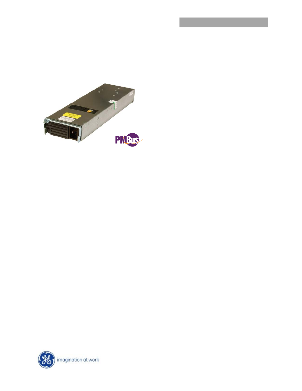
CAR1812FP series dc-dc converter
Input: 85Vac to 264Vac; Output: 12Vdc @ 1800W; 3.3Vdc or 5 Vdc @ 1A
Features
Universal input with PFC
Constant power characteristic
2 front panel LEDs: 1-input;2-[output, fault, over temp]
Remote ON/OFF control of the 12Vdc output
Remote sense on the 12Vdc output
No minimum load requirements
Redundant parallel operation
Active load sharing (single wire)
Hot Plug-ability
Efficiency: typically 92% @ 50% load
Standby orderable either as 3.3Vdc or 5Vdc
Auto recoverable OC & OT protection
Digital status & control: I
EN/IEC/UL60950-1 2
EMI: class B FCC docket 20780 part 15, EN55022
Meets EN6100 immunity and transient standards
Shock & vibration: NEBS GR-63-CORE, level 3
Applications
12Vdc distributed power architectures
Datacom applications
Mid to high-end Servers
Enterprise Networking
Network Attached Storage
Telecom Access Nodes
Routers/Switches
Data Sheet
2
C and PMBus serial bus
nd
edition; UL, CSA and VDE
Broadband Switches
ATE Equipment
Description
The CAR1812FP series of rectifiers provide highly efficient isolated power from worldwide input mains in a compact
1U industry standard form factor in an unprecedented power density of 21.7W/in
datacom applications such as enterprise networking, mid to high-end servers, and storage equipment, where mid to
light load efficiency is of key importance given the nature of the power consumption of the end application.
The high-density, front-to-back airflow is designed for minimal space utilization and is highly expandable for future
growth. The industry standard PMBus compliant I
2
C communications buss offers a full range of control and
monitoring capabilities. The SMBAlert signal pin alerts customers automatically of any state change within the power
supply.
November 1, 2012 ©2012 General Electric Company. All rights reserved.
3
. These rectifiers are ideal for
Page 2
GE Energy
CAR1812FP series dc-dc converter
Input: 85Vac to 264Vac; Output: 12 Vdc @ 1800W; 3.3Vdc or 5 Vdc @ 1A
Absolute Maximum Ratings
Stresses in excess of the absolute maximum ratings can cause permanent damage to the device. These are absolute stress ratings only, functional
operation of the device is not implied at these or any other conditions in excess of those given in the operations sections of the data sheet.
Exposure to absolute maximum ratings for extended periods can adversely affect the device reliability.
Parameter Device Symbol Min Max Unit
Input Voltage: Continuous
Operating Ambient Temperature TA -10 601 °C
Storage Temperature Tstg -40 85 °C
All
I/O Isolation voltage to Frame (100% factory Hi-Pot tested) 1500 Vac
Electrical Specifications
Unless otherwise indicated, specifications apply over all operating input voltage, load, and temperature conditions.
INPUT
Parameter Device Symbol Min Typ Max Unit
Operational Range
Frequency Range (ETSI 300-132-1 recommendation)
Main Output Turn_OFF
Maximum Input Current VIN= 100Vac
(VO= V
, IO=I
O, set
Cold Start Inrush Current
(Excluding x-caps, 25C, <10ms, per ETSI 300-132)
Efficiency [230Vac / 110Vac] 100% load
(T
=25C, V
amb
[230Vac / 110Vac] 20% load
Power Factor (Vin=230Vac, IO=I
Holdup time2 Vin= 220Vac
(Vout= 12V
Early warning prior output falling below 10.8Vdc Vin= 220V
Ride through T 10 ms
Leakage Current (Vin= 250Vac, Fin = 60Hz) I
Isolation Input/Output
Input/Frame 1500 V
Output/Frame 100 V
12Vdc MAIN OUTPUT
Output Power High Line Operation 180 – 264 Vac
Low Line Operation 90 – 132 Vac 0 - 1200 W
Set point
Overall regulation (load, temperature, aging) -3 +3 %
Ripple and noise3 120 mV
Turn-ON overshoot +3 %
Turn-ON delay T 2 sec
) VIN= 180Vac
O, max
= 12Vdc, IO=I
out
, Tamb 25C, IO=I
dc
) [230Vac / 110Vac] 50% load
O, max
) PF 0.99
O, max
) Vin= 100Vac
O, max
Parameter Device Symbol Min Typ Max Unit
All
ac
Vin= 100Vac
All
VIN 0 264 Vac
VIN 90 110/230 264 Vac
F
IN
V
IN
I
IN
I
IN
47 50/60 63 Hz
80 V
14.3
12.5
Aac
40 A
92 / 89
94 / 91
%
92 / 88
T
IN
3 mArms
10
15
ms
2
4
ms
3000 V
W
0 - 1800 W
11.9 12.00 12.1 V
V
out
ac
peak
ac
ac
dc
dc
p-p
1
Derated above 50C at 2.5%/C
2
12V output can decay down to 10.8V
3
Measured across a 10µf electrolytic and a 0.1µf ceramic capacitors in parallel. 20MHz bandwidth
November 1, 2012 ©2012 General Electric Company. All rights reserved. Page 2
Page 3
GE Energy
CAR1812FP series dc-dc converter
Input: 85Vac to 264Vac; Output: 12 Vdc @ 1800W; 3.3Vdc or 5 Vdc @ 1A
12Vdc MAIN OUTPUT (continued)
Parameter Device Symbol Min Typ Max Unit
Remote ON/OFF delay time
Turn-ON rise time (10 – 90% of V
)
out
Transient response 50% step [10%-60%, 50% - 100%]
(dI/dt – 1A/µs, recovery 300µs)
Programmable range (hardware & software) 10.8 13.2
Overvoltage protection, latched
All
V
out
(recovery by cycling OFF/ON via hardware or software)
Output current Vin = HL
V
Current limit, Hiccup (programmable level) 110 135 % of FL
= LL
in
I
out
Active current share -5 +5 % of FL
STANDBY OUTPUT
Parameter Device Symbol Min Typ Max Unit
Set point
Overall regulation (load, temperature, aging) V
Ripple and noise 50 mVp-p
Output current I
All
Overload protection -
Overvoltage protection
Isolation Output/Frame 100
V
3.3 / 5.0 V
stb
-5 +5 %
stb
out
Environmental, Reliability
Parameter Min Typ Max Units Notes
Ambient Temperature Operating
Altitude Operating
Power Derating
Storage
Altitude non-operating
Overload Protection shutdown
restart
Humidity Operating
Storage
Shock and Vibration acceleration 6 Grms NEBS GR-63-CORE, Level 3, 20 -2000Hz, minimum 30 minutes
Earthquake Rating 4
Reliability 25C
50C
200,000 Hrs Full load, demonstrated MTBF
Audible Noise 45
4
705
-10
-40
125
110
30
95
10
320,000
100,000
2250
2.5
85
8200
95
°C
m
%/°C
°C m
°C
%
Zone
Hrs
Hrs
Dba
Air inlet from sea level to 5,000 feet.
7400 ft
51°C to 70C (60C max where TUV/VDE is required)
30,000 ft
Relative humidity, non-condensing
NEBS GR-63-CORE, all floors, Seismic Zone 4 Designed and
tested to meet NEBS specifications.
Full load, MTBF per Bellcore RPP
Full load, MTBF per Bellcore RPP
25C, half load. Fan speed controlled
40 ms
50 ms
-5 +5 %V
V
dc
13.8 15.8
0
0
150
100
0 1 A
V
dc
A
dc
dc
dc
V
dc
out
4
Designed to start at an ambient down to -40°C; meet spec after 30 min warm up period, may not meet operational limits below -10°C.
5
60C max where TUV/VDE is required
November 1, 2012 ©2012 General Electric Company. All rights reserved. Page 3
Page 4

GE Energy
CAR1812FP series dc-dc converter
Input: 85Vac to 264Vac; Output: 12 Vdc @ 1800W; 3.3Vdc or 5 Vdc @ 1A
EMC
Parameter Criteria Standard Level Test
AC input Conducted emissions EN55022, FCC Docket 20780 part 15, subpart J
EN61000-3-2
Radiated emissions EN55022 A* 30 – 10000MHz
Voltage dips EN61000-4-11 B -30%, 10ms
B -60%, 100ms
B -100%, 5sec
Voltage surge EN61000-4-5 A 4kV, 1.2/50µs, common mode
A 2kV, 1.2/50µs, differential mode
immunity Fast transients EN61000-4-4 B 5/50ns, 2kV (common mode)
Enclosure immunity Conducted RF fields EN61000-4-6 A 130dBµV, 0.15-80MHz, 80% AM
Radiated RF fields EN61000-4-3 A 10V/m, 80-1000MHz, 80% AM
ENV 50140 A
ESD EN61000-4-2 B 4kV contact, 8kV air
* Note: Contact the factory for a recommended external EMI filter to meet Class B emissions
Status and Control
Some functions have two means of monitor/control; A
signal level that represents the analog value being
measured or controlled, or, reading/writing via the i
port the measured value or the control command.
Unless otherwise noted, control via the signals pins is
‘active’ so long that a firmware based command is not
initiated. Once firmware initiates a command that is also
represented on a signal pin, the firmware takes over and
replaces the hardware based control signal. Firmware
control is maintained until bias power to the processor is
interrupted. Once bias power is removed the processor
resets and the analog signal pin control is ‘active’ until
firmware takes over control.
Details of analog controls are provided in this data sheet
under Signal Definitions. GE Energy will provide separate
application notes on the I2C protocol. Contact your local
GE Energy representative for details.
2
C
Signal Definitions
All signals and outputs are referenced to Output return.
These include ‘Vstb return’ and ‘Signal return’.
Input Signals
Load share (Ishare): This is a single wire analog signal
that is generated and acted upon automatically by power
supplies connected in parallel. The Ishare pins should be
tied together for power supplies if active current share
among the power supplies is desired. No resistors or
capacitors should get connected to this pin.
Remote ON/OFF: Controls the presence of the main
12Vdc output voltage. This is an open collector, TTL level
control signal. This signal needs to be pulled HI
externally through a resistor. Maximum collector voltage
is 12Vdc and the maximum sink current is 4mA. A Logic
1 (TTL HI level) turns ON the 12Vdc output, while a Logic
0 (TTL LO level) turns OFF the 12Vdc output.
This signal is not overwritten by the firmware ON/OFF
instruction. The default firmware setting is ON. An OFF
command either through this signal or firmware would
turn OFF the power supply.
The default state re-initializes if bias power is interrupted
to the processor.
Enable: This is a short signal pin that controls the
presence of the 12Vdc main output. This pin should be
connected to ‘output return’ on the system side of the
output connector. The purpose of this pin is to ensure
that the output turns ON after engagement of the power
blades and turns OFF prior to disengagement of the
power blades.
Write protect (WP): This signal protects the contents of
the EEPROM from accidental over writing. When left
open the EEPROM is write protected. A LO (TTL
compatible) permits writing to the EEPROM. This signal
is pulled HI internally by the power supply.
Output signals
AC OK: A TTL compatible status signal representing
whether the input voltage is within the anticipated range.
This signal needs to be pulled HI externally through a
resistor. Maximum sink current ≤ 4mA and the max
voltage is 12Vdc. Open collector (HI) on this signal
indicates that the input voltage is applied within the
specified input range.
A* 0.15 – 30MHz
0 – 2 KHz
November 1, 2012 ©2012 General Electric Company. All rights reserved. Page 4
Page 5

GE Energy
CAR1812FP series dc-dc converter
Input: 85Vac to 264Vac; Output: 12 Vdc @ 1800W; 3.3Vdc or 5 Vdc @ 1A
DC OK: A TTL compatible status signal representing
whether the output voltage is present. This signal is
internally pulled HI to 3.3V via a 10kΩ resistor. Maximum
sink current ≤ 4mA and the max voltage is 12Vdc. Open
collector (HI) on this signal indicates that the output
voltage is present.
Fault: A TTL compatible status signal representing
whether a Fault occurred. This signal needs to be pulled
HI externally through a resistor. Maximum sink current ≤
4mA and the max voltage is 12Vdc. Open collector (HI)
on this signal indicates that no Fault is present.
This signal activates for OTP, OVP, OCP, AC fault or No
output.
PS Present: This pin is connected to ‘output return’ within
the power supply. Its intent is to indicate to the system
that a power supply is present. This signal may need to
be pulled HI externally through a resistor.
SMBAlert: A TTL compatible status signal, representing
the SMBusAlert# feature of the PMBus compatible i
protocol in the power supply. This signal needs to be
pulled HI externally through a resistor. Maximum sink
current ≤ 4mA and the pull up resistor should be tied to
3.3Vdc. Open collector (HI) on this signal indicates that
no Interrupt has been triggered.
2
C
Serial Bus Communications
The I²C interface facilitates the monitoring and control of
various operating parameters within the unit and
transmits these on demand over an industry standard I²C
Serial bus.
All signals are referenced to ‘Signal Return’.
Device addressing: The microcontroller (MCU) and the
EEPROM have the following addresses:
Device Address Address Bit Assignments
MCU 0xBx 1 0 1 1 A2 A1 A0 R/W
EEPROM 0xAx 1 0 1 0 A2 A1 A0 R/W
Address lines (A2, A1, A0): These signal pins allow up to
eight (8) modules to be addressed on a single I²C bus.
The pins are pulled HI internal to the power supply. For a
logic LO these pins should be connected to ‘Output
Return’
(Most to Least Significant)
Serial Clock (SCL): The clock pulses on this line are
generated by the host that initiates communications
across the I²C Serial bus. This signal is pulled up
internally to 3.3V by a 10kΩ resistor. The end user
should add additional pull up resistance as necessary to
ensure that rise and fall time timing and the maximum
sink current is in compliance to the I²C specifications.
Serial Data (SDA): This line is a bi-directional data line. .
This signal is pulled up internally to 3.3V by a 10kΩ
resistor. The end user should add additional pull up
resistance as necessary to ensure that rise and fall time
timing and the maximum sink current is in compliance to
the I²C specifications.
EEPROM
The microcontroller has 96 bytes of EEPROM memory
available for the system host.
Another separate EEPROM IC will provide another 128
bytes of memory with write protect feature. Minimum
information to be included in this separate EEPROM:
model number, revision, date code, serial number etc.
See the communications protocol for further information.
Communications Protocol
The I²C protocol is described in detail by the I2C and
PMBus Serial Communications Protocol for the CAR
Family of Power Supplies application note.
LEDs
Two LEDs are located on the front faceplate. The AC_OK
LED provides visual indication of the INPUT signal
function. When the LED is ON GREEN the power supply
input is within normal design limits.
The second LED DC/FLT provides visual indication of
three different states of the power supply. When the LED
is GREEN then there are no faults and the DC output is
present. When the LED is AMBER then a fault condition
exists but the power supply still provides output power.
When the LED is RED then a fault condition exists and
the power supply does not provide output power.
November 1, 2012 ©2012 General Electric Company. All rights reserved. Page 5
Page 6

GE Energy
CAR1812FP series dc-dc converter
Input: 85Vac to 264Vac; Output: 12 Vdc @ 1800W; 3.3Vdc or 5 Vdc @ 1A
Alarm Table
LED Indicator Monitoring Signals
LED1
Test Condition
1 Normal Operation
2 Low or NO INPUT Off
3 OVP
4 Over Current
5 Temp Alarm Warning
6 Fault Over Temp
7 Remote ON/OFF
Note: Test condition #2 had 2 modules plug in. One module is running and the other one is with no AC.
INPUT OK
Green Green
Green Red
Green Red
Green Orange
Green Red
Green Red
Tri-Color LED2
DC OK
Red
FAULT DC OK INPUT OK TEMP OK
High High High High
Low Low Low High
Low Low High High
Low Low High High
Low High High Low
Low Low High Low
Low Low High High
Outline Drawing
November 1, 2012 ©2012 General Electric Company. All rights reserved. Page 6
Page 7

GE Energy
CAR1812FP series dc-dc converter
Input: 85Vac to 264Vac; Output: 12 Vdc @ 1800W; 3.3Vdc or 5 Vdc @ 1A
Connector Pin Assignments
Input Connector: IEC320, C20 ; Mating connector: IEC320, C19
Output Connector: FCI Berg P/N: 51732-021 or equivalent
Mating connector: 51762-10802400ABLF (right angle mount)
Pin Function Pin Function Pin Function Pin Function
A1 Vstb B1 Fault C1 ISHARE D1 N/C
A2 Vstb Return B2 N/C C2 N/C D2 N/C
A3 Signal Return B3 Enable: “0” –ON “1” -OFF C3 N/C D3 Remote ON/OFF
A4 Write Protect (WP) B4 PS Present C4 I2C Address (A0) D4 DC OK
A5 Remote Sense (+) B5 SDA (I2C bus) C5 I2C Address (A1) D5 AC OK
A6 Remote Sense (-) B6 SCL (I2C bus) C6 I2C Address (A2) D6 SMBAlert
P1 - P4 Output Return P5 – P8 +Vout
Ordering Information
Please contact your GE Energy Sales Representative for pricing, availability and optional features.
PRODUCT DESCRIPTION PART NUMBER
1800W Front-End +12Vout DC INPUT Front-End w/Bezel, 3.3Vstb CAR1812FPBXXZ01A
1800W Front-End +12Vout AC INPUT Front-End w/o Bezel, 5Vstb CAR1812FPXX5Z01A
Contact Us
For more information, call us at
USA/Canada:
+1 888 546 3243, or +1 972 244 9288
Asia-Pacific:
+86.021.54279977*808
Europe, Middle-East and Africa:
+49.89.878067-280
India:
+91.80.28411633
November 1, 2012 ©2012 General Electric Company. All rights reserved. Page 7
www.ge.com/powerelectronics
 Loading...