

Page 1
GE
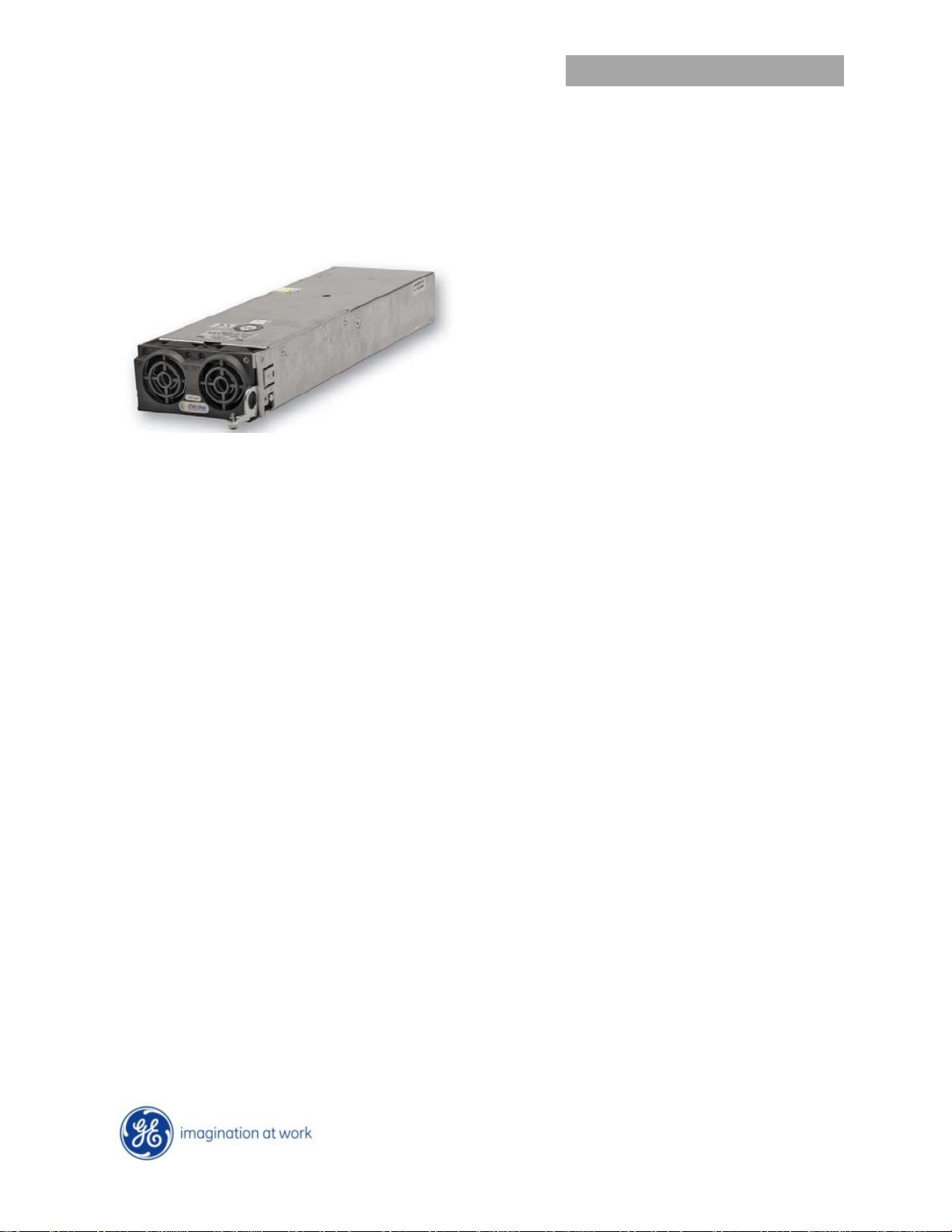
CAR1248TN series rectifier
Input: 90Vac to 264Vac; Output: -54Vdc @ 1200W
Applications
-48Vdc distributed power architectures
Cellular Base Stations
Blade Servers
Network Equipment
Network Attached Storage
Telecom Access Nodes
Preliminary Data Sheet
Features
Universal input with PFC
Constant power characteristic
3 front panel LEDs: 1-input;2-output; 3 - fault
Remote ON/OFF control of the -54Vdc output
Remote sense on the -54Vdc output
No minimum load requirements
Redundant parallel operation
Active load sharing (single wire)
Hot Plug-ability
Efficiency: typically 91% @ 50% load
Auto recoverable OC & OT protection
Operating temperature: 0 - 70C (de-rated above 50C)
Digital status & control: I
EN/IEC/UL60950-1 2
EMI: class A FCC docket 20780 part 15, EN55022
Meets EN6100 immunity and transient standards
Shock & vibration: NEBS GR-63-CORE, level 3
2
C serial bus
nd
edition; UL, CSA and VDE
Routers/Switches
Broadband Switches
ATE Equipment
Description
The CAR1248TN series of rectifiers provide highly efficient isolated -54Vdc power from worldwide input mains in a
compact density of 19W/in
The high-density, front-to-back airflow is designed for minimal space utilization and is highly expandable for future
2
growth. I
C communications offers remote control and monitoring capabilities.
3
within a 1U industry standard form factor.
November 20, 2012 ©2012 General Electric Company. All rights reserved.
Page 2
GE
CAR1248TN series rectifier
Input: 90Vac to 264Vac; Output: -54Vdc @ 1200W
Absolute Maximum Ratings
Stresses in excess of the absolute maximum ratings can cause permanent damage to the device. These are absolute stress ratings only, functional
operation of the device is not implied at these or any other conditions in excess of those given in the operations sections of the data sheet.
Exposure to absolute maximum ratings for extended periods can adversely affect the device reliability.
Parameter Device Symbol Min Max Unit
Input Voltage: Continuous
Operating Ambient Temperature TA -10 701 °C
Storage Temperature T
All
I/O Isolation voltage to Frame (100% factory Hi-Pot tested) 1500 Vac
Electrical Specifications
Unless otherwise indicated, specifications apply over all operating input voltage, load, and temperature conditions.
INPUT
Parameter Device Symbol Min Typ Max Unit
Operational Range
Frequency Range
Main Output Turn_OFF
Maximum Input Current VIN= 180Vac
(VO= V
, IO=I
O, set
Cold Start Inrush Current
(Excluding x-caps, 25C, <10ms, per ETSI 300-132)
Efficiency Vin= 230V
(T
=25C, V
amb
Power Factor
=230Vac, IO=I
(V
in
Holdup time Vin= 230Vac
(V
= -54Vdc, T
out
Early warning prior to loss of DC output below regulation 2 ms
Ride through T 8.3 ms
Leakage Current
(V
= 250Vac, Fin = 60Hz)
in
Isolation Input/Output
Input/Frame 1500 V
Output/Frame 500 V
-54Vdc MAIN OUTPUT
Output Power High Line Operation 180 – 264 Vac
Low Line Operation 90 – 132Vac 0 - 1000 W
Set point
Overall regulation (load, temperature, aging) -3 +3 %
Ripple and noise2 540
32 dBrnc
Turn-ON overshoot +3 %
) VIN= 100Vac
O, max
= -54Vdc, IO=I
out
)
O, max
25C, IO=I
amb
) Vin= 90V
O, max
) Vin= 90Vac
O, max
Parameter Device Symbol Min Typ Max Unit
ac
ac
All
All
VIN 0 264 Vac
-40 85 °C
stg
VIN 90 110/230 264 Vac
F
IN
V
IN
I
IN
I
IN
47 50/60 63 Hz
70 80 V
40 A
90
85
7.9
12.75
Aac
peak
%
ac
PF 0.99
T
I
IN
3 mA
3000 V
W
0 - 1200 W
-53.9 -54.00 -54.1 V
V
out
16.7
20
ms
rms
ac
ac
dc
dc
mV
p-p
1
Derated above 50C at 2.5%/C
2
Measured across a 10µf electrolytic and a 0.1µf ceramic capacitors in parallel. 20MHz bandwidth
November 20, 2012 ©2012 General Electric Company. All rights reserved. Page 2
Page 3
GE
CAR1248TN series rectifier
Input: 90Vac to 264Vac; Output: -54Vdc @ 1200W
-54Vdc MAIN OUTPUT (continued)
Parameter Device Symbol Min Typ Max Unit
Turn-ON delay
Remote ON/OFF delay time 40 ms
Turn-ON rise time (10 – 90% of V
)
out
T
Transient response 50% step [10%-60%, 50% - 100%]
(dI/dt – 1A/µs, recovery 300µs)
V
out
Programmable range (hardware & software) -42 -58
Overvoltage protection, latched
(reset by cycling OFF/ON via hardware or software)
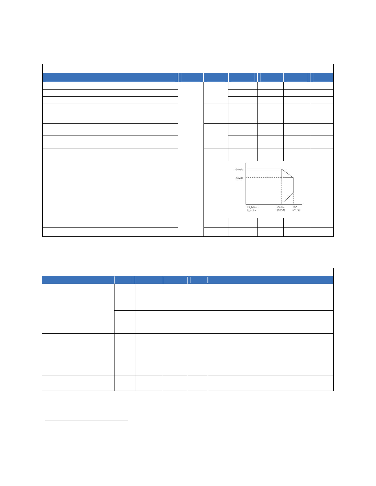
Output current Vin – high line
V
– low line
in
Power/Current limit Vin – high line
V
– low line
in
All
I
out
P
out
Power limit down to -48Vdc
2 sec
50 ms
-5 +5 %V
-58 -59 -60
0
22.2
18.5
1200
1000
out
V
dc
V
dc
A
dc
W
Current limit below -48Vdc, Hiccup (programmable level)
Active current share
I
out
I
out
113 130
-10 +10 % of FL
Environmental, Reliability
Parameter Min Typ
Ambient Temperature
Operating
Altitude Operating
Power Derating
Storage
Altitude non-operating
Over Temperature Protection 120 / 110 °C Shutdown / Restart
Humidity Operating
Storage
Shock and Vibration acceleration
Earthquake Rating 4
MTBF
3
-10
-40
30
95
10
100,000
200,000
Max Units
50
2250
2.5
85
8200
95
6
°C
m
%/°C
°C m
%
Grms
Zone
Hrs
Air inlet from sea level to 5,000 feet.
7400 ft
51°C to 70C
30,000 ft
Relative humidity, non-condensing
NEBS GR-63-CORE, Level 3, 20 -2000Hz, minimum 30
minutes
NEBS GR-63-CORE, all floors, Seismic Zone 4 Designed and
tested to meet NEBS specifications.
Full load, 50C ambient, per Bellcore RPP
Demonstrated
% of FL
Notes
3
The unit will start up at -40C but is not guaranteed to meet specification limits until it is within the operating ambient range.
November 20, 2012 ©2012 General Electric Company. All rights reserved. Page 3
Page 4
GE
CAR1248TN series rectifier
Input: 90Vac to 264Vac; Output: -54Vdc @ 1200W
EMC
Parameter Criteria Standard Level Test
AC input Conducted emissions EN55022, FCC Docket 20780 part 15, subpart J A 0.15 – 30MHz
Radiated emissions** EN55022 A 30 – 10000MHz
Voltage dips EN61000-4-11 A -30%, 10ms
B -60%, 100ms
B -100%, 5sec
Voltage surge EN61000-4-5 A 4kV, 1.2/50µs, common mode
A 2kV, 1.2/50µs, differential mode
immunity Fast transients EN61000-4-4 B 5/50ns, 2kV (common mode)
Enclosure immunity Conducted RF fields EN61000-4-6 A 130dBµV, 0.15-80MHz, 80% AM
Radiated RF fields EN61000-4-3 A 10V/m, 80-1000MHz, 80% AM
ENV 50140 A
ESD EN61000-4-2 B 4kV contact, 8kV air
** Radiated emissions compliance is contingent upon the final system configuration.
Status and Control
Signal Definitions
All signals and outputs are referenced to Output return. These
include ‘Vstb return’ and ‘Signal return’.
Input Signals
Voltage programming (V
can vary the output voltage from -42Vdc to -58Vdc. The
equation of this signal is:
V
out
= 20x (V
) 2.1 < V
prog
If Vprog is ≥ 4V, or left open the programming signal is ignored
and the unit output is set at the setpoint of -54Vdc.
Load share (Ishare): Single wire analog signal between power
supplies connected in parallel. The Ishare pins should be tied
together for power supplies. No resistors or capacitors should
get connected to this pin.
Remote ON/OFF: Controls the presence of the main -54Vdc
output voltage. This is an open collector, TTL level control
signal. This signal needs to be pulled HI externally through a
resistor. Maximum collector voltage is 12Vdc, maximum sink
current is 1mA. Logic 1 turns ON the -54Vdc output, while a
Logic 0 turns OFF the -54Vdc output.
A turn OFF command either through this signal or firmware
commanded would turn OFF the -54V output.
Enable: This is a short signal pin that controls the presence of
the -54Vdc main output. This pin should be connected to
‘output return’ on the system side of the output connector. The
purpose of this pin is to ensure that the output turns ON after
engagement of the power blades and turns OFF prior to
disengagement of the power blades.
Write protect (WP): This signal protects the contents of the
external EEPROM. When left open the EEPROM is write
): An analog voltage on this signal
prog
< 2.9
prog
protected. A LO permits writing to the EEPROM. This signal is
pulled HI internally by the power supply.
Output signals
Output current monitor (Imon): A voltage level proportional to
the output current is present on this pin. The signal level is
0. 2V per amp ± 0.25V.
AC OK: TTL compatible open collector. Maximum sink current
20mA, max voltage is 12Vdc. A (HI) on this signal indicates
that the input voltage is present within limits.
DC OK: TTL compatible, open collector. Maximum sink
current 20mA, max voltage is 12Vdc. A (HI) on this signal
indicates that the output voltage is present.
Over temp warning: TTL compatible, open collector.
Maximum sink current 20mA, max voltage is 12Vdc. A (HI) on
this signal indicates that temperatures are normal.
If an over temperature should occur, this signal would delay
pulling LO for approximately 10 seconds. The unit would
restart if internal temperatures recover within normal
operational levels.
Fault: TTL compatible, open collector. Maximum sink current
20mA, max voltage is 12Vdc. A (HI) on this signal indicates
that no faults are present.
This signal activates for OTP, OVP, or AC fault.
PS Present: Connected to ‘output return’. Its intent is to
indicate to the system that a power supply is present. This
signal may need to be pulled HI externally through a resistor.
Interrupt: A TTL compatible status signal, representing the
SMBusAlert# feature of the i
This signal needs to be pulled HI externally through a resistor.
Maximum sink current ≤ 4mA and the pull up resistor should
be tied to <5Vdc. Open collector (HI) on this signal indicates
that no Interrupt has been triggered.
2
C protocol in the power supply.
November 20, 2012 ©2012 General Electric Company. All rights reserved. Page 4
Page 5
GE
CAR1248TN series rectifier
Input: 90Vac to 264Vac; Output: -54Vdc @ 1200W
Serial Bus Communications – CAR1248TN
The I²C interface facilitates the monitoring and control of
various operating parameters within the unit and transmits
these on demand over an industry standard I²C Serial bus.
All signals are referenced to ‘Signal Return’.
Device addressing: The microcontroller (MCU) and the
EEPROM have the following addresses:
Device Address Bit Assignments
MCU 1 0 1 1 A2 A1 A0 R/W
EEPROM 1 0 1 0 A2 A1 A0 R/W
Address lines (A2, A1, A0): Up to eight (8) modules to be
addressed on a single I²C bus. The pins are pulled HI internal
to the power supply. For a logic LO connect to ‘Output Return’
Serial Clock (SCL): Host generated, this signal needs to be
pulled up externally ensuring that rise and fall time timing and
the maximum sink current is in compliance to the I²C
specification.
Serial Data (SDA): This is a bi-directional line that needs to be
pulled up externally ensuring that rise and fall time timing and
the maximum sink current is in compliance to the I²C
specification.
Command code:
All registers are 16 bits, written as LSB followed by MSB.
All A/D’s are 10 bit (1024 steps). All constants can be fine-tuned
to compensate for manufacturing tolerances;
Name CMD Access Default
Vout 00 R -54 0.102
Iout 01 R - 0.042
Temperature 02 R - 0.005
ON/OFF 03 R/W 1 – OFF, 0 – ON
Ilimit 04 R/W 25 0.042
Vset 05 R/W -54 0.094
Vprog 06 R Vout= 20 x Vprog
OT trip 07 R/W 120 0.005
OT recover 08 R/W 110 0.005
DC_OK_HI 09 R/W 55.6 0.102
DC_OK_LO 0A R/W 52.4 0.102
STATUS 0B R
Firmware 0C R
EEPROM 0D-
(Most to Least Significant)
Bits Constant
/Name
Input 0 1-LL
AC_OK 1
DC_OK 2
OT 3
Fault 4
Intrpt 5
OV 6
DC_INT 7
R/W
7C
1-normal
Vout [00]: Output voltage read back, returns the voltage on
the anode side of the or’ing function, data LSB followed by
MSB.
The default value is -54Vdc
Example; readback 0211h, convert into its decimal equivalent
and then multiply by the constant, Vout = 529 x 0.102 =
54Vdc
Iout [01]: Output current read back, data LSB followed by MSB.
Example; readback 021Fh, convert into its decimal equivalent
and multiply by the constant, Iout=543 x 0.042 = 22.8A
Temperature [02]: Temperature read back, data LSB followed
by MSB.
Example; readback 037Bh, convert into its decimal equivalent
and multiply by the constant, temp = 891 x 0.005 = 4.36. In the
table below this corresponds to 25C
Data Temp
C
4.83 -5 3.71 45 1.7 95
4.78 0 3.51 50 1.54 100
4.72 5 3.3 55 1.4 105
4.65 10 3.09 60 1.26 110
4.56 15 2.88 65 1.14 115
4.46 20 2.67 70 1.03 120
4.35 25 2.46 75 0.93 125
4.21 30 2.25 80 0.84 130
4.06 35 2.06 85
3.89 40 1.88 90
Data Temp
C
Data Temp
C
ON/OFF [03]: A logic ‘1’ turns OFF the -54V output of the
power supply.
Ilim [04]: This feature lowers the current limit from the default
values of 0253h (595), corresponding to 25A at high line and
01EFh (495) corresponding to 20.8A at low line.
The delivered output current cannot exceed the maximum
power capacity of the unit. At high line the power supply is
limited to 1200W, thus, at -48Vdc the output current is limited
to 25A.
Example: At high line, reduce the current limit to 20A.
Compute the data to be sent to the controller; 20 / 0.042 =
476. The hex equivalent of this decimal data is 01DCh. The
data should be sent across the bus as LSB [DC] followed by
MSB [01].
Vset [05]: Changes the output voltage via i2c, if the Vprog
hardware signal is > 4Vdc. If the Vprog pin voltage level is <
4Vdc, this command is ignored.
The output voltage setting must be between -42 – -58Vdc.
The default value is 023Eh, corresponding to -54Vdc.
Example; set the output to 48Vdc. Compute the data to be
sent to the controller; 48 / 0.094 = 510. The hex equivalent of
this decimal data is 01FEh. The data should be sent across the
bus as LSB [FE] followed by MSB [01].
November 20, 2012 ©2012 General Electric Company. All rights reserved. Page 5
Page 6
GE
CAR1248TN series rectifier
Input: 90Vac to 264Vac; Output: -54Vdc @ 1200W
Vprog [06]; Reads back the hardware configured analog
voltage program value via i2c.
The value of Vprog can range from 2.1V to 2.8V.
Example: set the output to 44Vdc. From the equation
determine that Vprog = 2.2. The 10bit D/A is set for the range
of 0 – 5Vdc, therefore with a resolution of 1024 bits each bit is
0.00488V. So the corresponding value to enter is 2.2/0.00488 =
451 decimal. This corresponds to 01C3h. The data should be
sent across the bus as LSB [C3] followed by MSB [01].
OT trip[07] and OT recover[08]; Configures the OT shutdown
and recovery levels. The default values are;
OT trip: 120C corresponds to 1.03/0.005 = D3h
OT recover: 110C that corresponds to 1.26/0.00488 = 0102h
Example: Change the recovery temperature to 100C. In the
look up table above the corresponding level is 1.54. Divide by
the conversion ration, 1.54/0.00488 = 315 dec. Converting to
its hex equivalent yields 013B hex. The data should be sent
across the bus as LSB [3B] followed by MSB [01].
DC_OK_HI[09] and DC_OK_LO[0A]: Changes the DC_OK signal
comparator level. The default values are;
DC_OK_HI: 0221h, corresponding to 55.6V
DC_OK_LO: 0201h, corresponding to 52.4V
Example: Change the upper level of comparison to 55V.
Determine the corresponding register value setting; 55/0.102
= 539dec. This is equivalent to 021Bh. The data should be
sent across the bus as LSB [1B] followed by MSB [02].
STATUS [0B]: All read backs are two bytes and so read back
two bytes but ignore the MSB.
Firmware [0C]: Reads back the latest firmware revision.
MCUeeprom [0D – 7C]: 125 bytes of information may be
stored in the EEPROM section of the micro controller starting
from register location 0Dh. Each byte of data needs to be
stored into its specific register location, one byte at a time.
External EEPROM
A separate EEPROM, with its own i2c address and with
write_protect capability, provides 128 bytes of memory. This is
a standard i2c compliant generic EEPROM with a single byte
for its memory location. Standard i2c command structure
applies.
The following FRU_ID information is stored in this EEPROM
Start
Location
00h 7 Serial number, ascii
07h 1 20h space
08h 4 Date code [YYWW] ascii
0Ch 1 20h space
0Dh 17
1Eh 1 20h space
1Fh 1 Revision
Length Value Description
Code CAR1248TNBXXZ01A ascii
LEDs
Three LEDs are located on the front faceplate. The AC_OK LED
provides visual indication of the INPUT signal function. When
the LED is ON GREEN the power supply input is within normal
design limits.
When the DC_OK LED is GREEN the DC output is present.
When the FAULT_LED is RED then a fault condition exists and
the power supply may not provide output power. The table
below further defines these states:
Alarm Table
LED Indicator Monitoring Signals
Test Condition
1 Normal Operation
2 Low or NO INPUT OFF OFF OFF High Low Low High
3 OVP
4 Over Current
5 Over Temp Fault
Note: Test condition #2 has 2 modules working in parallel. One module is running and the other has no AC.
November 20, 2012 ©2012 General Electric Company. All rights reserved. Page 6
AC OK DC OK FAULT FAULT DC OK AC OK TEMP OK
Green Green
Green
Green
Green
OFF
OFF
OFF
OFF High High High High
Red
Red
Red
Low Low High High
High Low High High
Low Low High Low
Page 7
GE
CAR1248TN series rectifier
Input: 90Vac to 264Vac; Output: -54Vdc @ 1200W
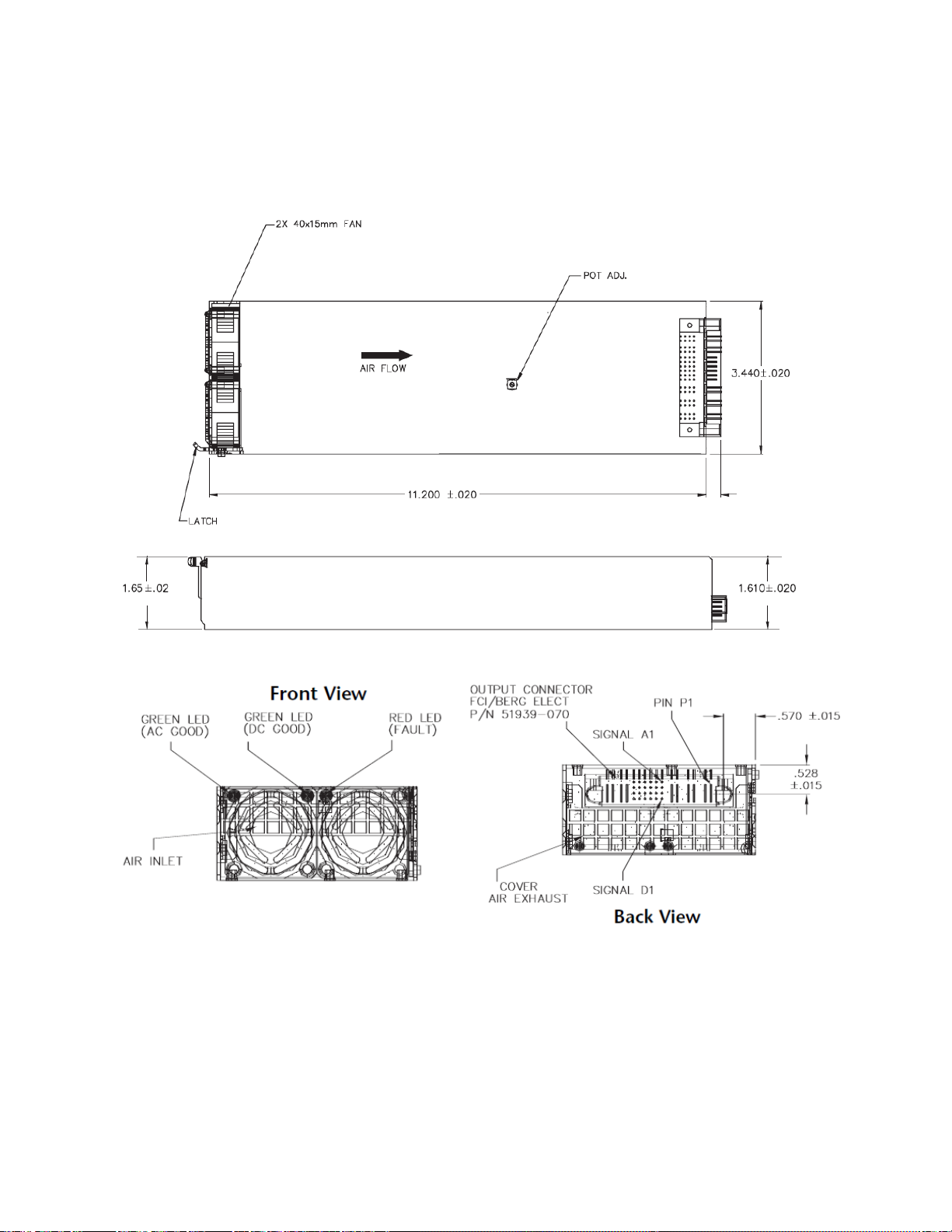
Outline Drawing
November 20, 2012 ©2012 General Electric Company. All rights reserved. Page 7
Page 8

GE
CAR1248TN series rectifier
Input: 90Vac to 264Vac; Output: -54Vdc @ 1200W
Connector
FCI Berg P/N: 51939-070
Mating connector: FCI Berg P/N: 51915-050
Pin Function Pin Function Pin Function Pin Function
A1 n/c B1 Fault C1 ISHARE D1 VProg
A2 n/c B2 I Monitor (IMON) C2 N/C D2 OVP Test Point
A3 Signal Return B3 Enable: “0” –ON “1” -OFF C3 Over Temp Warning D3 Remote ON/OFF
A4 Write Protect (WP) B4 PS Present C4 I2C Address (A0) D4 DC OK
A5 Remote Sense (+) B5 SDA (I2C bus) C5 I2C Address (A1) D5 AC OK
A6 Remote Sense (-) B6 SCL (I2C bus) C6 I2C Address (A2) D6 Interrupt
P1 Line P2 Neutral P3 Chassis
P4 +Vout P5 Output Return
Ordering Information
Please contact your GE Energy Sales Representative for pricing, availability and optional features.
PRODUCT DESCRIPTION PART NUMBER
1200W Front-End -54Vout Front-End CAR1248TNXXXZ01A
1200W Front-End -54Vout Front-End, w/bezel CAR1248TNBXXZ01A
1200W Front-End -54Vout Front-End, w/bezel, i2c communications CAR1248TNBCXZ01A
Contact Us
For more information, call us at
USA/Canada:
+1 888 546 3243, or +1 972 244 9288
Asia-Pacific:
+86.021.54279977*808
Europe, Middle-East and Africa:
+49.89.878067-280
India:
+91.80.28411633
www.ge.com/powerelectronics
November 20, 2012 ©2012 General Electric Company. All rights reserved. Page 8
 Loading...