

Page 1
SERVICE MANUAL
32" COLOR LCD TELEVISION
LCD-A3206/LCD-B3206/
LCD-C3206/LCD-D3206
Page 2

32″ COLOR LCD TELEVISION
LCD-A3206/LCD-B3206/
LCD-C3206/LCD-D3206
TABLE OF CONTENTS
Specifications . . . . . . . . . . . . . . . . . . . . . . . . . . . . . . . . . . . . . . . . . . . . . . . . . . . . . . . . . . . . . . . . . . . . . . . . . . . 1-1
Important Safety Precautions. . . . . . . . . . . . . . . . . . . . . . . . . . . . . . . . . . . . . . . . . . . . . . . . . . . . . . . . . . . . . . . 2-1
Standard Notes for Servicing . . . . . . . . . . . . . . . . . . . . . . . . . . . . . . . . . . . . . . . . . . . . . . . . . . . . . . . . . . . . . . . 3-1
Cabinet Disassembly Instructions . . . . . . . . . . . . . . . . . . . . . . . . . . . . . . . . . . . . . . . . . . . . . . . . . . . . . . . . . . . 4-1
How to Initialize the LCD Television. . . . . . . . . . . . . . . . . . . . . . . . . . . . . . . . . . . . . . . . . . . . . . . . . . . . . . . . . . 5-1
Electrical Adjustment Instructions . . . . . . . . . . . . . . . . . . . . . . . . . . . . . . . . . . . . . . . . . . . . . . . . . . . . . . . . . . . 6-1
Block Diagrams . . . . . . . . . . . . . . . . . . . . . . . . . . . . . . . . . . . . . . . . . . . . . . . . . . . . . . . . . . . . . . . . . . . . . . . . . 7-1
Schematic Diagrams / CBA’s and Test Points . . . . . . . . . . . . . . . . . . . . . . . . . . . . . . . . . . . . . . . . . . . . . . . . . . 8-1
Waveforms . . . . . . . . . . . . . . . . . . . . . . . . . . . . . . . . . . . . . . . . . . . . . . . . . . . . . . . . . . . . . . . . . . . . . . . . . . . . . 9-1
Wiring Diagram . . . . . . . . . . . . . . . . . . . . . . . . . . . . . . . . . . . . . . . . . . . . . . . . . . . . . . . . . . . . . . . . . . . . . . . . 10-1
Exploded View . . . . . . . . . . . . . . . . . . . . . . . . . . . . . . . . . . . . . . . . . . . . . . . . . . . . . . . . . . . . . . . . . . . . . . . . . 11-1
Mechanical Parts List . . . . . . . . . . . . . . . . . . . . . . . . . . . . . . . . . . . . . . . . . . . . . . . . . . . . . . . . . . . . . . . . . . . . 12-1
Electrical Parts List. . . . . . . . . . . . . . . . . . . . . . . . . . . . . . . . . . . . . . . . . . . . . . . . . . . . . . . . . . . . . . . . . . . . . . 13-1
The LCD panel is manufactured to provide many years of useful life.
Occasionally a few non active pixels may appear as a tiny spec of color.
This is not to be considered a defect in the LCD screen.
Page 3
SPECIFICATIONS
< TUNER >
ANT. Input -----------------------75 ohm Unbal., F type
Reference Level ---------------20 Vp-p (LCD Green Cathode)
Test Input Signal---------------400 Hz 30% modulation
Description Condition Unit Nominal Limit
1. Intermediate Freq.
2. Color Killer Sens.
3. AFT Pull In Range (10 mV input) --- MHz ±2.4 ±2.1
Picture
Sound
CH-2
CH-10
CH-55
MHz
MHz
dBµV
dBµV
dBµV
45.75
41.25
17
17
17
---
---
23
23
23
< LCD PANEL >
Description Condition Unit Nominal Limit
1. Number of Pixels
2. Brightness cd/m
3. Response Time (tr+tf) --- msec 25 ---
4. Support Color --- - 16.7 mil. (8 bit) ---
5. Viewing Angle
Horizontal
Ver ti ca l
Horizontal
Ver ti ca l
pixels
pixels
°
°
1366× 3
768
2
470 ---
-85 to 85
-85 to 85
---
---
---
---
< VIDEO >
Description Condition Unit Nominal Limit
1. Over Scan
2. Color Temperature
3. Resolution
Horizontal
Ver ti ca l
--x
y
Horizontal
Ver ti ca l
%
%
°K
line
line
5
5
12000
0.272
0.278
400
350
---
---
--±0.03
±0.03
---
---
< AUDIO >
All items are measured across 8 Ω load at speaker output terminal with L.P.F.
Description Condition Unit Nominal Limit
1. Audio Output Power 10% THD: Lch/Rch W 5.0/5.0 4.5/4.5
2. Audio Distortion 500mW: Lch/Rch % 1.0/1.0 4.0/4.0
-
3. Audio Freq. Response
Note: Nominal specifications represent the design specifications. All units should be able to approximate these.
Some will exceed and some may drop slightly below these specifications. Limit specifications represent
the absolute worst condition that still might be considered acceptable. In no case should a unit fail to meet
limit specifications.
6dB: Lch
-
6dB: Rch
Hz
Hz
100 to 10 k
100 to 10 k
---
---
1-1 L5920SP
Page 4
IMPORTANT SAFETY PRECAUTIONS
Prior to shipment from the factory, our products are strictly inspected for recognized product safety and electrical
codes of the countries in which they are to be sold. However, in order to maintain such compliance, it is equally
important to implement the following precautions when a set is being serviced.
Safety Precautions for LCD TV
Circuit
1. Before returning an instrument to the
customer, always make a safety check of the
entire instrument, including, but not limited to, the
following items:
a. Be sure that no built-in protective devices are
defective and have been defeated during
servicing. (1) Protective shields are provided
on this chassis to protect both the technician
and the customer. Correctly replace all missing
protective shields, including any removed for
servicing convenience. (2) When reinstalling
the chassis and/or other assembly in the
cabinet, be sure to put back in place all
protective devices, including but not limited to,
nonmetallic control knobs, insulating
fishpapers, adjustment and compartment
covers/shields, and isolation resistor/capacitor
networks. Do not operate this instrument or
permit it to be operated without all
protective devices correctly installed and
functioning. Servicers who defeat safety
features or fail to perform safety checks
may be liable for any resulting damage.
b. Be sure that there are no cabinet openings
through which an adult or child might be able to
insert their fingers and contact a hazardous
voltage. Such openings include, but are not
limited to, (1) spacing between the LCD module
and the cabinet mask, (2) excessively wide
cabinet ventilation slots, and (3) an improperly
fitted and/or incorrectly secured cabinet back
cover.
c. Antenna Cold Check - With the instrument AC
plug removed from any AC source, connect an
electrical jumper across the two AC plug
prongs. Place the instrument AC switch in the
on position. Connect one lead of an ohmmeter
to the AC plug prongs tied together and touch
the other ohmmeter lead in turn to each tuner
antenna input exposed terminal screw and, if
applicable, to the coaxial connector. If the
measured resistance is less than 1.0 megohm
or greater than 5.2 megohm, an abnormality
exists that must be corrected before the
instrument is returned to the customer. Repeat
this test with the instrument AC switch in the off
position.
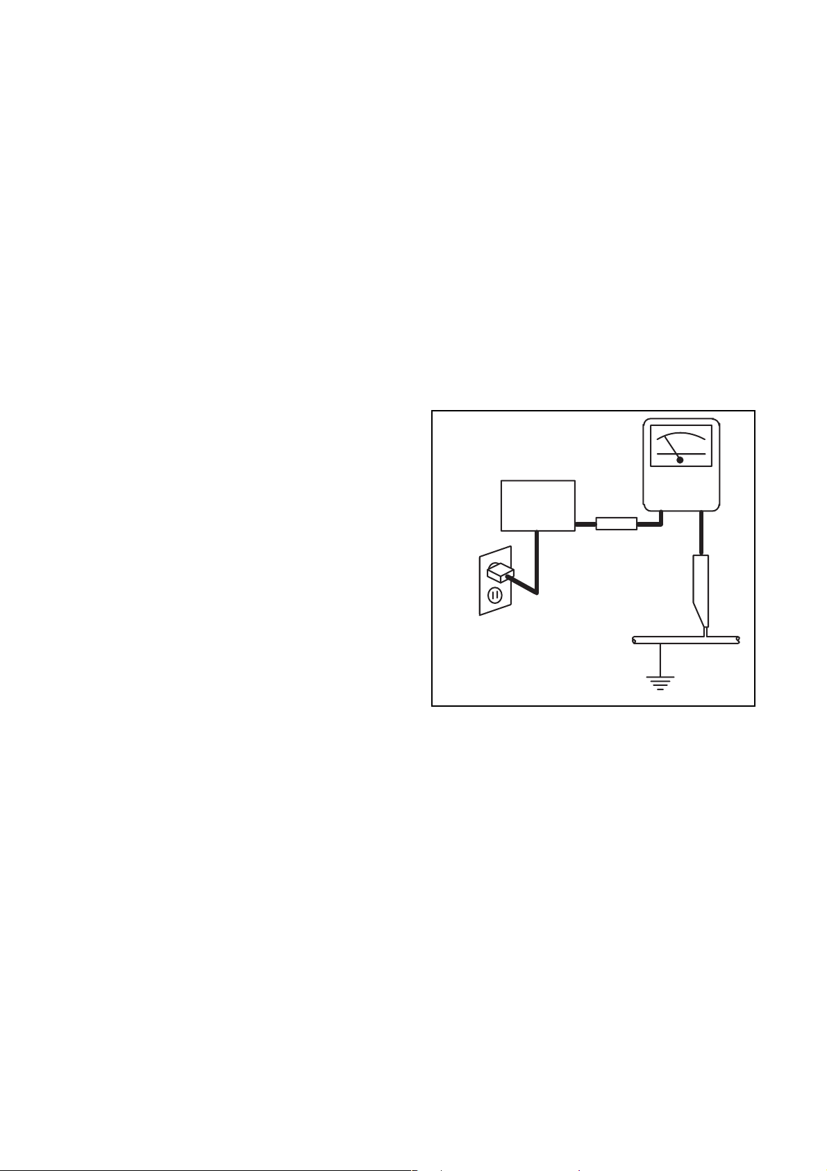
d. Leakage Current Hot Check - With the
instrument completely reassembled, plug the
AC line cord directly into a 230 V AC outlet. (Do
not use an isolation transformer during this
test.) Use a leakage current tester or a
metering system that complies with American
National Standards Institute (ANSI) C101.1
Leakage Current for Appliances and
Underwriters Laboratories (UL) 1410, (50.7).
With the instrument AC switch first in the on
position and then in the off position, measure
from a known earth ground (metal water pipe,
conduit, etc.) to all exposed metal parts of the
instrument (antennas, handle brackets, metal
cabinet, screw heads, metallic overlays, control
shafts, etc.), especially any exposed metal
parts that offer an electrical return path to the
chassis. Any current measured must not
exceed 0.5 milli-ampere. Reverse the
instrument power cord plug in the outlet and
repeat the test.
READING SHOULD
NOT BE ABOVE 0.5 mA
LEAKAGE
DEVICE
BEING
TESTED
TEST ALL EXPOSED
METAL SURFACES
ALSO TEST WITH
PLUG REVERSED
USING AC
ADAPTER PLUG
AS REQUIRED
ANY MEASUREMENTS NOT WITHIN THE
LIMITS SPECIFIED HEREIN INDICATE A
POTENTIAL SHOCK HAZARD THAT MUST
BE ELIMINATED BEFORE RETURNING THE
INSTRUMENT TO THE CUSTOMER OR
BEFORE CONNECTING THE ANTENNA OR
ACCESSORIES.
2. Read and comply with all caution and safety-
related notes on or inside the receiver cabinet, on
the receiver chassis, or on the LCD module.
3. Design Alteration Warning - Do not alter or add
to the mechanical or electrical design of this LCD
TV receiver. Design alterations and additions,
including, but not limited to circuit modifications
and the addition of items such as auxiliary audio
and/or video output connections, might alter the
safety characteristics of this receiver and create a
hazard to the user. Any design alterations or
additions will void the manufacturer's warranty and
may make you, the servicer, responsible for
personal injury or property damage resulting
therefrom.
CURRENT
TESTER
+
EARTH
GROUND
_
2-1 LTVP_ISP
Page 5

4. Hot Chassis Warning -
a. Some TV receiver chassis are electrically
connected directly to one conductor of the AC
power cord and maybe safety-serviced without
an isolation transformer only if the AC power
plug is inserted so that the chassis is
connected to the ground side of the AC power
source. To confirm that the AC power plug is
inserted correctly, with an AC voltmeter,
measure between the chassis and a known
earth ground. If a voltage reading in excess of
1.0V is obtained, remove and reinsert the AC
power plug in the opposite polarity and again
measure the voltage potential between the
chassis and a known earth ground.
b. Some TV receiver chassis normally have 85V
AC(RMS) between chassis and earth ground
regardless of the AC plug polarity. This chassis
can be safety-serviced only with an isolation
transformer inserted in the power line between
the receiver and the AC power source, for both
personnel and test equipment protection.
c. Some TV receiver chassis have a secondary
ground system in addition to the main chassis
ground. This secondary ground system is not
isolated from the AC power line. The two
ground systems are electrically separated by
insulation material that must not be defeated or
altered.
5. Observe original lead dress. Take extra care to
assure correct lead dress in the following areas: a.
near sharp edges, b. near thermally hot parts-be
sure that leads and components do not touch
thermally hot parts, c. the AC supply, d. high
voltage, and, e. antenna wiring. Always inspect in
all areas for pinched, out of place, or frayed wiring.
Check AC power cord for damage.
6. Components, parts, and/or wiring that appear to
have overheated or are otherwise damaged
should be replaced with components, parts, or
wiring that meet original specifications.
Additionally, determine the cause of overheating
and/or damage and, if necessary, take corrective
action to remove any potential safety hazard.
7. Product Safety Notice - Some electrical and
mechanical parts have special safety-related
characteristics which are often not evident from
visual inspection, nor can the protection they give
necessarily be obtained by replacing them with
components rated for higher voltage, wattage, etc..
Parts that have special safety characteristics are
identified by a ! on schematics and in parts lists.
Use of a substitute replacement that does not
have the same safety characteristics as the
recommended replacement part might create
shock, fire, and/or other hazards. The product's
safety is under review continuously and new
instructions are issued whenever appropriate.
Prior to shipment from the factory, our products
are strictly inspected to confirm they comply with
the recognized product safety and electrical codes
of the countries in which they are to be sold.
However, in order to maintain such compliance, it
is equally important to implement the following
precautions when a set is being serviced.
2-2 LTVP_ISP
Page 6

Precautions during Servicing
A. Parts identified by the ! symbol are critical for
safety.
Replace only with part number specified.
B. In addition to safety, other parts and assemblies
are specified for conformance with regulations
applying to spurious radiation. These must also be
replaced only with specified replacements.
Examples: RF converters, RF cables, noise
blocking capacitors, and noise blocking filters, etc.
C. Use specified internal wiring. Note especially:
1) Wires covered with PVC tubing
2) Double insulated wires
3) High voltage leads
D. Use specified insulating materials for hazardous
live parts. Note especially:
1) Insulation Tape
2) PVC tubing
3) Spacers
4) Insulators for transistors.
E. When replacing AC primary side components
(transformers, power cord, etc.), wrap ends of
wires securely about the terminals before
soldering.
F. Observe that the wires do not contact heat
producing parts (heat sinks, oxide metal film
resistors, fusible resistors, etc.)
G. Check that replaced wires do not contact sharp
edged or pointed parts.
H. When a power cord has been replaced, check that
5~6 kg of force in any direction will not loosen it.
I. Also check areas surrounding repaired locations.
J. Use care that foreign objects (screws, solder
droplets, etc.) do not remain inside the set.
K. Crimp type wire connector
The power transformer uses crimp type
connectors which connect the power cord and the
primary side of the transformer. When replacing
the transformer, follow these steps carefully and
precisely to prevent shock hazards.
Replacement procedure
1) Remove the old connector by cutting the wires
at a point close to the connector.
Important: Do not re-use a connector (discard
it).
2) Strip about 15 mm of the insulation from the
ends of the wires. If the wires are stranded,
twist the strands to avoid frayed conductors.
3) Align the lengths of the wires to be connected.
Insert the wires fully into the connector.
4) Use the crimping tool to crimp the metal sleeve
at the center position. Be sure to crimp fully to
the complete closure of the tool.
L. When connecting or disconnecting the internal
connectors, first, disconnect the AC plug from the
AC supply outlet.
M. When installing parts or assembling the cabinet
parts, be sure to use the proper screws and
tighten certainly.
2-3 LTVP_ISP
Page 7
Safety Check after Servicing
Examine the area surrounding the repaired location
for damage or deterioration. Observe that screws,
parts and wires have been returned to original positions. Afterwards, perform the following tests and confirm the specified values in order to verify compliance
with safety standards.
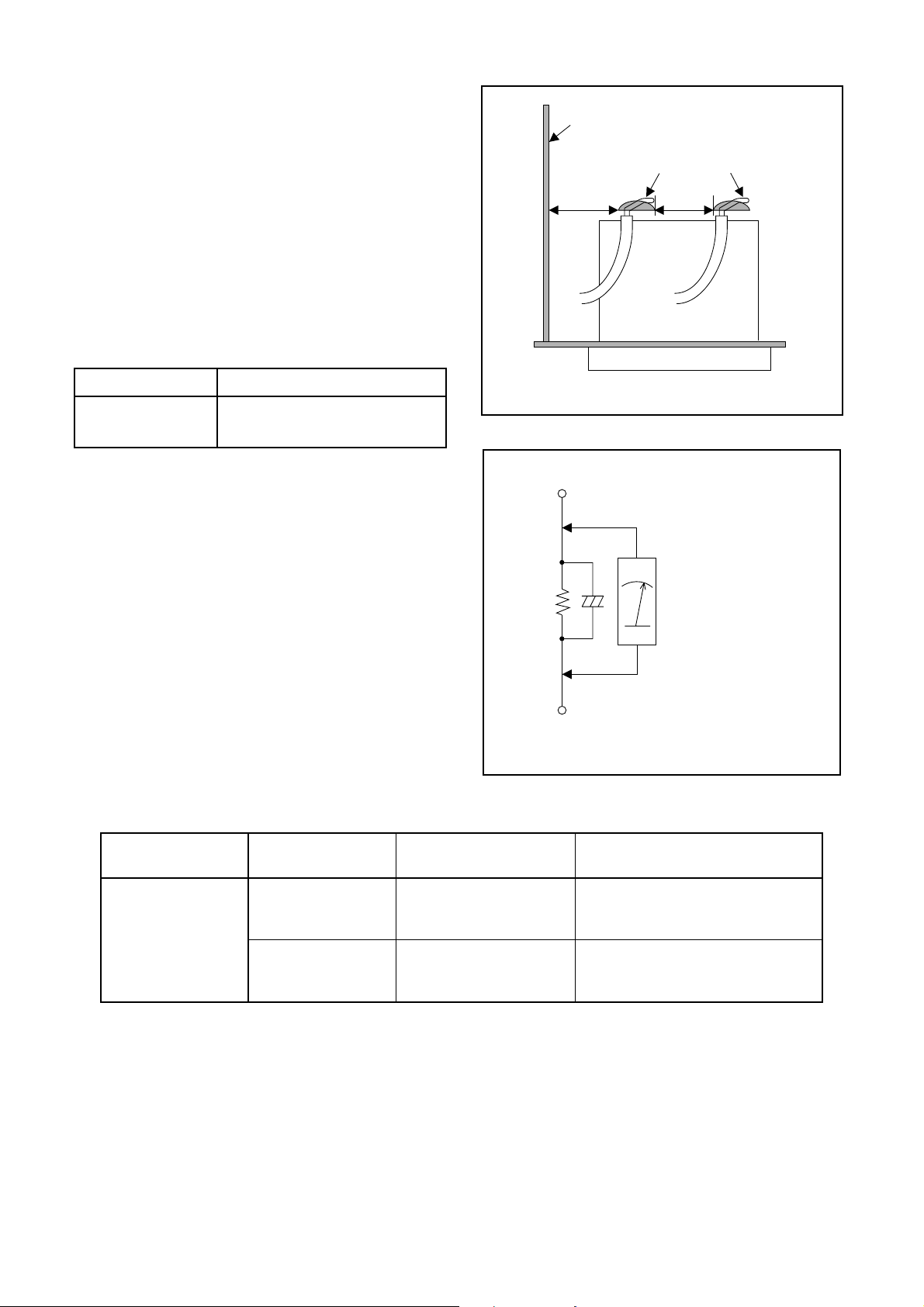
1. Clearance Distance
When replacing primary circuit components, confirm
specified clearance distance (d) and (d') between soldered terminals, and between terminals and surrounding metallic parts. (See Fig. 1)
Table 1 : Ratings for selected area
AC Line Voltage Clearance Distance (d), (d’)
230 V
Note: This table is unofficial and for reference only.
Be sure to confirm the precise values.
≥ 3mm(d)
≥ 6 mm(d’)
2. Leakage Current Test
Confirm the specified (or lower) leakage current between B (earth ground, power cord plug prongs) and
externally exposed accessible parts (RF terminals, antenna terminals, video and audio input and output terminals, microphone jacks, earphone jacks, etc.).
Chassis or Secondary Conductor
Primary Circuit
d' d
Exposed Accessible Part
Z
AC Voltmeter
(High Impedance)
Fig. 1
Measuring Method : (Power ON)
Insert load Z between B (earth ground, power cord
plug prongs) and exposed accessible parts. Use an
AC voltmeter to measure across both terminals of load
Z. See Fig. 2 and following table.
Table 2: Leakage current ratings for selected areas
AC Line Voltage Load Z Leakage Current (i)
2kΩ RES.
Connected in
parallel
230 V
50kΩ RES.
Connected in
parallel
Note: This table is unofficial and for reference only. Be sure to confirm the precise values.
i≤0.7mA AC Peak
i≤2mA DC
i≤0.7mA AC Peak
i≤2mA DC
One side of
B
Power Cord Plug Prongs
One side of power cord plug
prongs (B) to:
Antenna terminals
A/V Input, Output
Fig. 2
RF or
2-4 LTVP_ISP
Page 8
STANDARD NOTES FOR SERVICING
Circuit Board Indications
1. The output pin of the 3 pin Regulator ICs is
indicated as shown.
Top View
Out
2. For other ICs, pin 1 and every fifth pin are
indicated as shown.
Pin 1
3. The 1st pin of every male connector is indicated as
shown.
Pin 1
Input
In
Bottom View
5
10
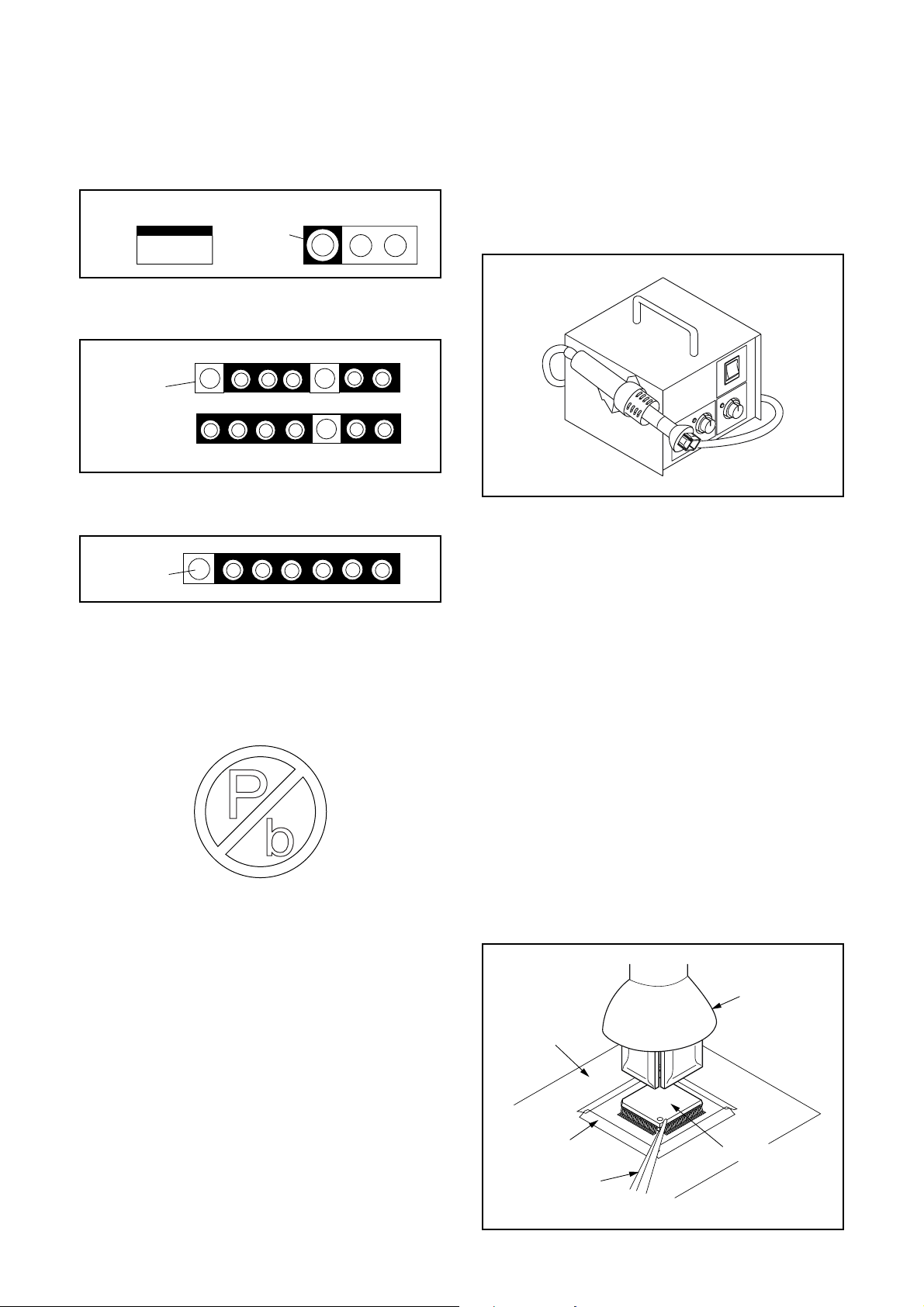
Pb (Lead) Free Solder
Pb free mark will be found on PCBs which use Pb
free solder. (Refer to figure.) For PCBs with Pb free
mark, be sure to use Pb free solder. For PCBs
without Pb free mark, use standard solder.
Pb free mark
How to Remove / Install Flat Pack-IC
1. Removal
With Hot-Air Flat Pack-IC Desoldering Machine:
1. Prepare the hot-air flat pack-IC desoldering
machine, then apply hot air to the Flat Pack-IC
(about 5 to 6 seconds). (Fig. S-1-1)
Fig. S-1-1
2. Remove the flat pack-IC with tweezers while
applying the hot air.
3. Bottom of the flat pack-IC is fixed with glue to the
CBA; when removing entire flat pack-IC, first apply
soldering iron to center of the flat pack-IC and heat
up. Then remove (glue will be melted). (Fig. S-1-6)
4. Release the flat pack-IC from the CBA using
tweezers. (Fig. S-1-6)
CAUTION:
1. The Flat Pack-IC shape may differ by models. Use
an appropriate hot-air flat pack-IC desoldering
machine, whose shape matches that of the Flat
Pack-IC.
2. Do not supply hot air to the chip parts around the
flat pack-IC for over 6 seconds because damage
to the chip parts may occur. Put masking tape
around the flat pack-IC to protect other parts from
damage. (Fig. S-1-2)
3. The flat pack-IC on the CBA is affixed with glue, so
be careful not to break or damage the foil of each
pin or the solder lands under the IC when
removing it.
Hot-air
Flat Pack-IC
Desoldering
CBA
Masking
Tape
Tweezers
3-1 TVP_SN
Machine
Flat Pack-IC
Fig. S-1-2
Page 9
With Soldering Iron:
1. Using desoldering braid, remove the solder from
all pins of the flat pack-IC. When you use solder
flux which is applied to all pins of the flat pack-IC,
you can remove it easily. (Fig. S-1-3)
Flat Pack-IC
Desoldering Braid
Soldering Iron
Fig. S-1-3
2. Lift each lead of the flat pack-IC upward one by
one, using a sharp pin or wire to which solder will
not adhere (iron wire). When heating the pins, use
a fine tip soldering iron or a hot air desoldering
machine. (Fig. S-1-4)
With Iron Wire:
1. Using desoldering braid, remove the solder from
all pins of the flat pack-IC. When you use solder
flux which is applied to all pins of the flat pack-IC,
you can remove it easily. (Fig. S-1-3)
2. Affix the wire to a workbench or solid mounting
point, as shown in Fig. S-1-5.
3. While heating the pins using a fine tip soldering
iron or hot air blower, pull up the wire as the solder
melts so as to lift the IC leads from the CBA
contact pads as shown in Fig. S-1-5.
4. Bottom of the flat pack-IC is fixed with glue to the
CBA; when removing entire flat pack-IC, first apply
soldering iron to center of the flat pack-IC and heat
up. Then remove (glue will be melted). (Fig. S-1-6)
5. Release the flat pack-IC from the CBA using
tweezers. (Fig. S-1-6)
Note: When using a soldering iron, care must be
taken to ensure that the flat pack-IC is not
being held by glue. When the flat pack-IC is
removed from the CBA, handle it gently
because it may be damaged if force is applied.
Sharp
Pin
Fine Tip
Soldering Iron
3. Bottom of the flat pack-IC is fixed with glue to the
CBA; when removing entire flat pack-IC, first apply
soldering iron to center of the flat pack-IC and heat
up. Then remove (glue will be melted). (Fig. S-1-6)
4. Release the flat pack-IC from the CBA using
tweezers. (Fig. S-1-6)
Fig. S-1-4
To Solid
Mounting Point
CBA
Hot Air Blower
or
Iron Wire
Soldering Iron
Fig. S-1-5
Fine Tip
Soldering Iron
Flat Pack-IC
Tweezers
Fig. S-1-6
3-2 TVP_SN
Page 10
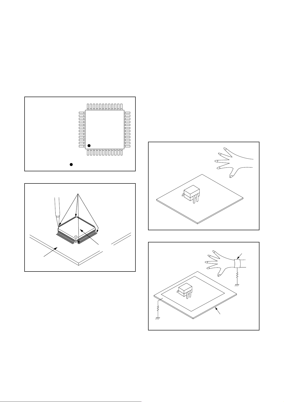
2. Installation
1. Using desoldering braid, remove the solder from
the foil of each pin of the flat pack-IC on the CBA
so you can install a replacement flat pack-IC more
easily.
2. The “●” mark on the flat pack-IC indicates pin 1.
(See Fig. S-1-7.) Be sure this mark matches the 1
on the PCB when positioning for installation. Then
presolder the four corners of the flat pack-IC. (See
Fig. S-1-8.)
3. Solder all pins of the flat pack-IC. Be sure that
none of the pins have solder bridges.
Example :
Pin 1 of the Flat Pack-IC
is indicated by a " " mark.
Fig. S-1-7
Instructions for Handling Semiconductors
Electrostatic breakdown of the semi-conductors may
occur due to a potential difference caused by
electrostatic charge during unpacking or repair work.
1. Ground for Human Body
Be sure to wear a grounding band (1 MΩ) that is
properly grounded to remove any static electricity that
may be charged on the body.
2. Ground for Workbench
Be sure to place a conductive sheet or copper plate
with proper grounding (1 MΩ) on the workbench or
other surface, where the semi-conductors are to be
placed. Because the static electricity charge on
clothing will not escape through the body grounding
band, be careful to avoid contacting semi-conductors
with your clothing.
<Incorrect>
CBA
Presolder
Flat Pack-IC
Fig. S-1-8
<Correct>
1MΩ
CBA
Grounding Band
1MΩ
CBA
Conductive Sheet or
Copper Plate
3-3 TVP_SN
Page 11
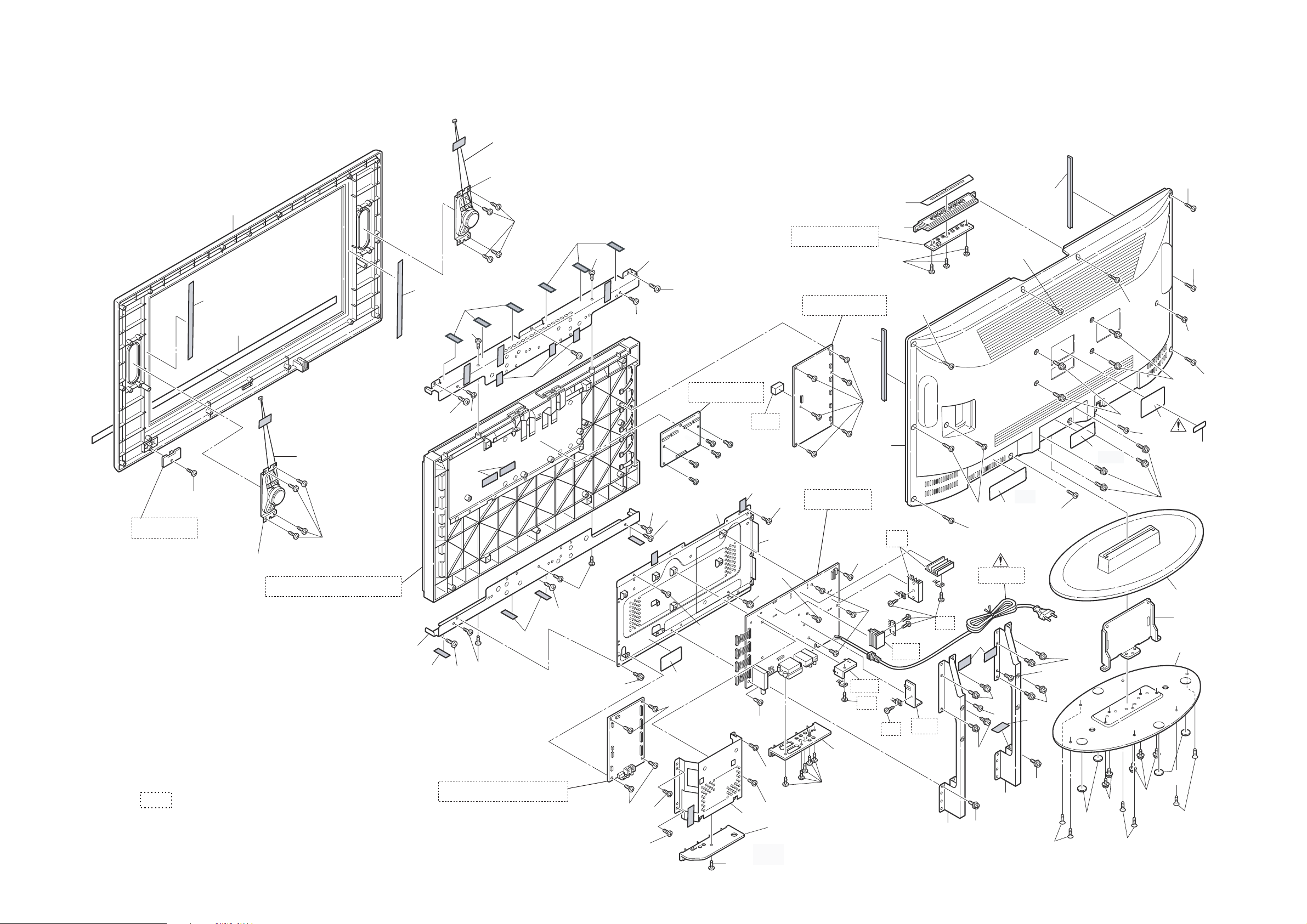
CABINET DISASSEMBLY INSTRUCTIONS
1. Disassembly Flowchart
This flowchart indicates the disassembly steps for the
cabinet parts, and the CBA in order to gain access to
item(s) to be serviced. When reassembling, follow the
steps in reverse order. Bend, route and dress the
cables as they were.
[1] Stand Base
Plate
[2] Stand Hinge
[18] Speaker (R)
[7] Jack Holder(D)
[9] Shield Box
[11] Digital Main
CBA Unit
[3] Stand Cover
[4] Rear Cabinet
[6] Chassis Bracket
[8] Jack Holder(A)
[10] Main CBA
[13] PCB Holder
[14] Panel Holder
[16] LCD Module Assembly
[20] Front Cabinet
[19] Speaker (L)
[5] Function CBA
[17] LED CBA
[12] Inverter CBA
[15] T-CON CBA
2. Disassembly Method
Removal
Step/
Loc.
Part
No.
Stand Base
[1]
Plate
Stand
[2]
Hinge
Stand
[3]
Cover
Rear
[4]
Cabinet
Function
[5]
CBA
Chassis
[6]
Bracket
Jack
[7]
Holder(D)
Jack
[8]
Holder(A)
[9] Shield Box D2 4(S-11) ---
Remove/*Unhook/
Fig.
No.
Unlock/Release/
Unplug/Unclamp/
Note
Desolder
D1 4(S-1), 6(S-2), 5(S-3) ---
D1 --------------- ---
D1 --------------- ---
D1 12(S-4), 4(S-5) ---
D1D53(S-6), *CN10, *CN11,
*CN11B
D2 10(S-7), 2(S-8) ---
D2 (S-9) ---
D2 5(S-10) ---
---
Removal
Step/
Loc.
No.
Part
Remove/*Unhook/
Fig.
No.
Unlock/Release/
Unplug/Unclamp/
Note
Desolder
6(S-12), *CN54,
[10] Main CBA
D3
*CN103A, *CN104A,
D5
---
*CN101A, *CN102A,
*CN703
Digital Main
[11]
CBA UnitD3D5
4(S-13), *CN111,
*CN400
---
6(S-14), *CN1050,
[12]
Inverter
CBA
D3
*CN1100, *CN1150,
D5
*CN1150, *CN1200,
---
*CN1250, CN1300
[13] PCB Holder D3 2(S-15), 2(S-16) ---
Panel
[14]
[15]
Holder
T-CON
CBA
D4 6(S-17), 9(S-18) ---
5(S-19), *CN211,
D4
*CN212, *CN213,
D5
*CN214
---
LCD
[16]
Module
D4 --------------- ---
Assembly
[17] LED CBA D4 (S-20) ---
Speaker
[18]
(R)
D4 4(S-21) ---
[19] Speaker (L) D4 4(S-22) ---
Front
[20]
↓
(1)
Cabinet
↓
(2)
D4 --------------- ---
↓
(3)
↓
(4)
↓
(5)
Note:
(1) Order of steps in procedure. When reassembling,
follow the steps in reverse order. These numbers
are also used as the Identification (location) No. of
parts in figures.
(2) Parts to be removed or installed.
(3) Fig. No. showing procedure of part location
(4) Identification of parts to be removed, unhooked,
unlocked, released, unplugged, unclamped, or
desoldered.
N = Nut, L = Locking Tab, S = Screw,
CN = Connector
* = Unhook, Unlock, Release, Unplug, or Desolder
e.g. 2(S-2) = two Screws (S-2),
2(L-2) = two Locking Tabs (L-2)
(5) Refer to the following "Reference Notes in the
Ta b le . "
4-1 L5920DC
Page 12
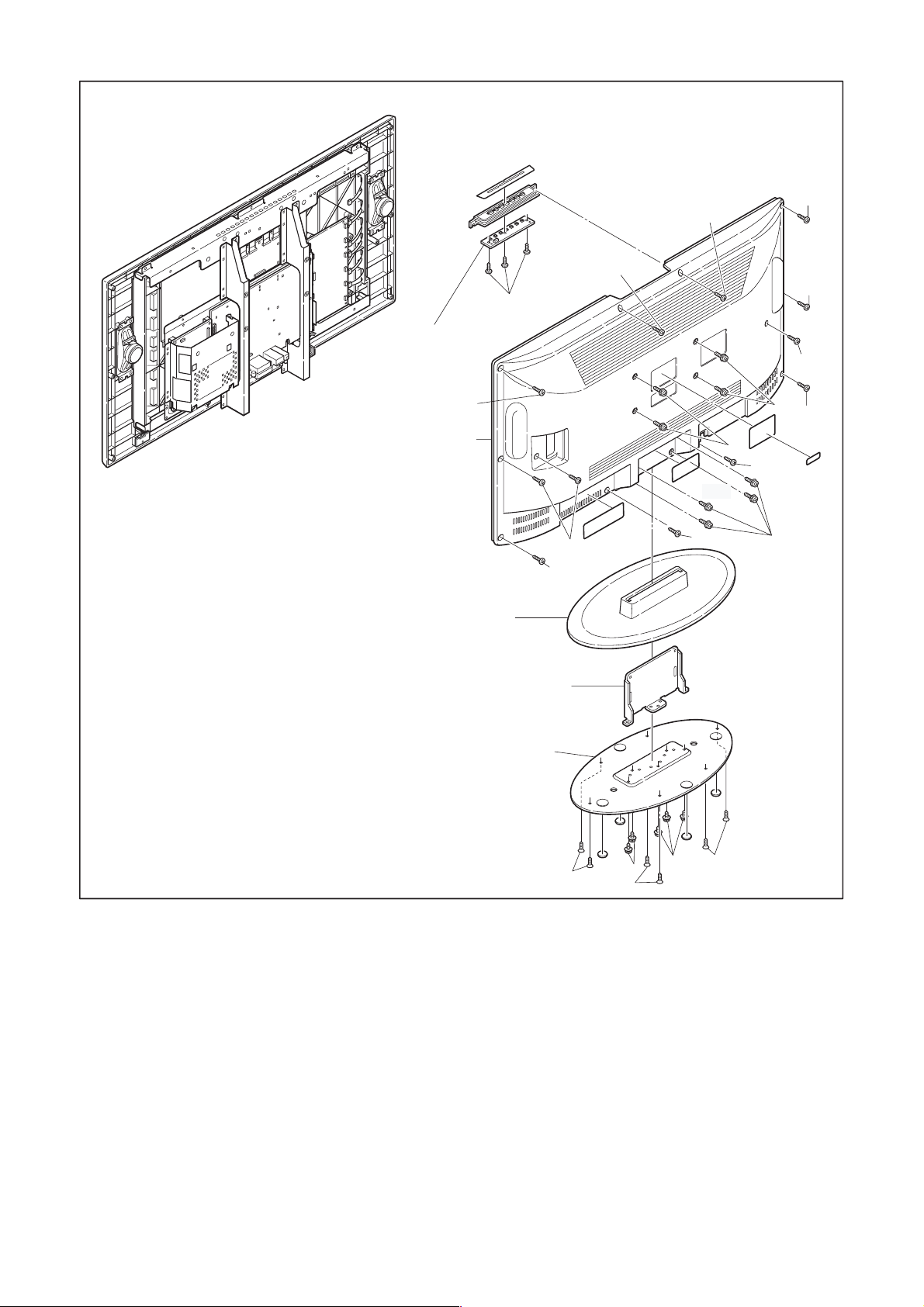
S-6
[5] Function CBA
S-4
S-4
S-4
S-4
S-4
S-4
[4] Rear Cabinet
[3] Stand Cover
[2] Stand Hinge
[1] Stand Base Plate
S-4
S-4
S-4
S-5
S-4
S-5
S-1
S-4
S-3
S-2
S-3
S-2
S-2
Fig. D1
4-2 L5920DC
Page 13
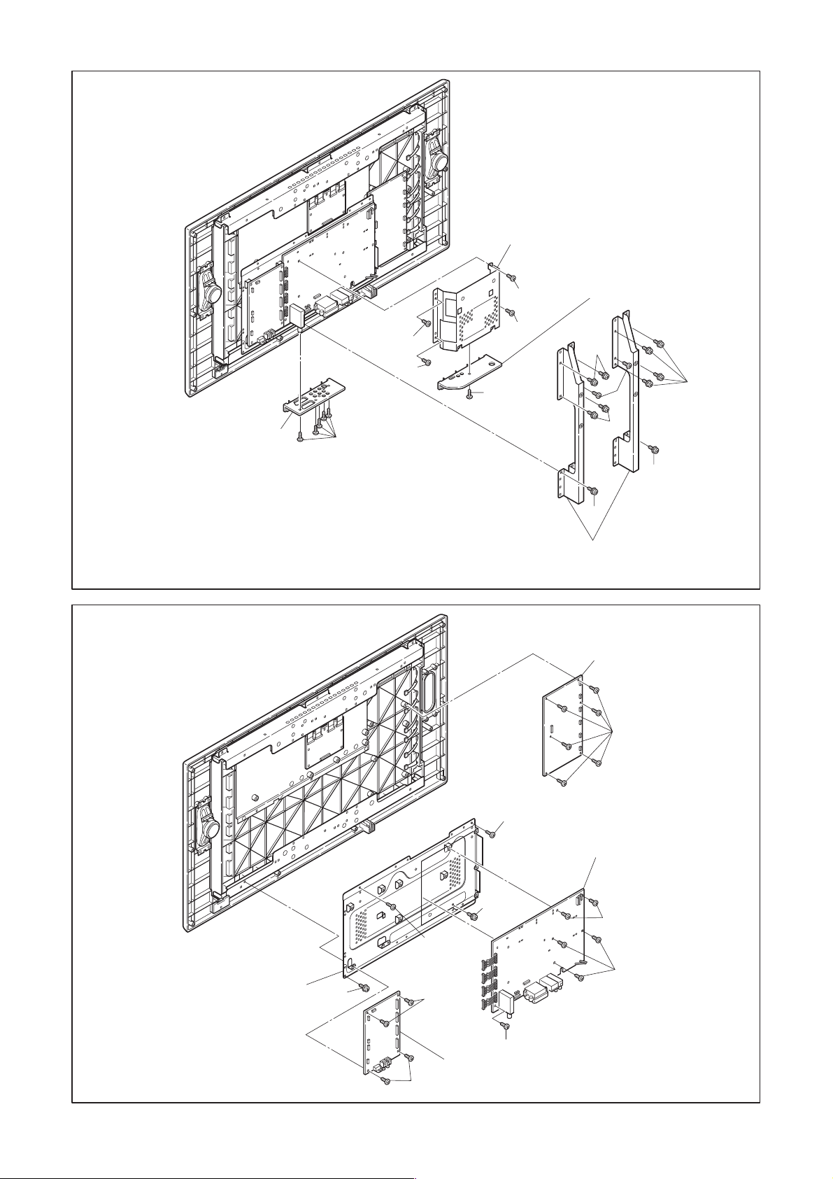
[9] Shield Box
[8] Jack Holder(A)
S-10
S-11
S-11
S-9
S-11
S-11
[7] Jack Holder(D)
S-7
S-7
[6] Chassis Bracket
[12] Inverter CBA
S-7
S-8
S-7
S-7
Fig. D2
[13] PCB Holder
S-16
S-15
S-16
S-15
S-13
S-12
[11] Digital Main CBA Unit
S-13
S-14
[10] Main CBA
S-12
S-12
Fig. D3
4-3 L5920DC
Page 14
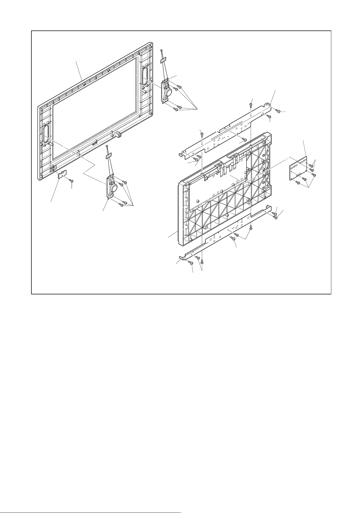
[20] Front Cabinet
[18] Speaker (R)
[14] Panel Holder
S-18
S-20
[17] LED CBA
S-22
[19] Speaker (L)
[16] LCD Module Assembly
[14] Panel Holder
S-17
S-18
S-17
S-21
S-18
S-18
S-17
S-18
[15] T-CON CBA
S-17
S-19
S-19
S-17
S-18
S-18
S-17
Fig. D4
4-4 L5920DC
Page 15
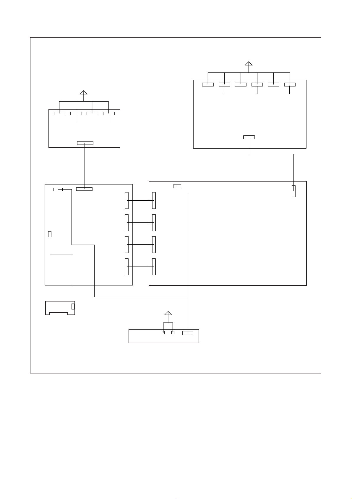
TV Cable Wiring Diagram
To LCD
Module Assembly
To LCD
Module Assembly
CN214
CN211
CN213
CN111
T-CON CBA
CN11A
CN111
CN400
CN212
Digital Main
CBA Unit
CN101B
CN102B
CN103B
Inverter CBA
Main CBA
CN101A
CN102A
CN103A
CN54
CN1050
CN1100
CN1000
CN1150
CN1200
CN1250
CN1300
CN703
LED CBA
CN54B
CN104B
Function CBA
CN104A
To Speaker
CN10
CN11
CN11B
Fig. D5
4-5 L5920DC
Page 16

HOW TO INITIALIZE THE LCD TELEVISION
To put the program back at the factory-default,
initialize the LCD television as the following procedure.
How to initialize the LCD television:
1. Turn the power off.
2. To enter the service mode, while pressing
[SETUP] button, press [STANDBY-ON] button on
the TV unit.
- To cancel the service mode, press [STANDBY-
ON] button on the remote control.
3. To initialize the LCD television, press “DISPLAY”
button on the remote control unit.
4. Confirm "FF" indication on the upper left of the
screen.
5-1 L5820INT
Page 17
ELECTRICAL ADJUSTMENT INSTRUCTIONS
General Note:
“CBA” is abbreviation for “Circuit Board Assem-
bly.”
NOTE:
Electrical adjustments are required after replacing
circuit components and certain mechanical parts. It is
important to perform these adjustments only after all
repairs and replacements have been completed.
Also, do not attempt these adjustments unless the
proper equipment is available.
Test Equipment Required
1. DC Voltmeter
2. Pattern Generator
3. Color Analyzer
How to Set up the Service mode:
1. Turn the power off.
2. While pressing [SETUP] button, press [STANDBYON] button on the TV unit
- To cancel the service mode, press [STANDBY-ON]
button on the TV unit.
1. Initial Setting
General
Enter the Service mode.
Set the each initial data as shown on table 1 below.
Table 1: Initial Data
BUTTON
ITEM
D1-BRT
D1-CNT 128
D1-CLR-R 128
D1-CLR-B 128
D1-TNT 128
D1-SHR 70
D2-BRT
D2-CNT 128
D2-CLR-R 128
D2-CLR-B 128
D2-TNT 128
D2-SHR 70
D3-BRT
D3-CNT 128
D3-CLR-R 128
D3-CLR-B 128
D3-TNT 128
D3-SHR 40
D4-BRT
D4-CNT 128
D4-CLR-R 128
D4-CLR-B 128
D4-TNT 128
D4-SHR 40
BRT
CNT 170
CLR-R 128
CLR-B 128
TNT 128
SHR 45
S-BRT
S-CNT 170
S-CLR-R 128
S-CLR-B 128
S-TNT 128
S-SHR 45
C-BRT
C-CNT 128
C-CLR-R 128
C-CLR-B 128
C-TNT 128
C-SHR 70
(on the remote
control)
MENU → 1
MENU → 2
MENU → 3
MENU → 4
MENU → 5
MENU → 6
MENU → 7
DATA
VALUE
128
128
128
128
128
128
128
6-1 L5920EA
Page 18
DT-BRT
ITEM
BUTTON
(on the remote
control)
DATA
VALUE
128
DT-CNT 170
DT-CLR-R 128
DT-CLR-B 128
MENU → 8
DT-TNT 128
DT-SHR 45
BRIGHT 0 255
NORMAL 0 176
DARK 0 112
7F
LAST POWER ON
NCM ON
VOL. p
FF
XV100 OFF
*COR 1(C/D/S 1) VOL. p → 1 120
COG 1(C/D/S 1) VOL. p → 2 127
*COB 1(C/D/S 1) VOL. p → 3 131
*DR 1(C/D/S 1) VOL. p → 4 134
DG 1(C/D/S 1) VOL. p → 5 119
*DB 1(C/D/S 1) VOL. p → 6 114
SBR 1(C/D/S 1) VOL. p → 763
SBB 1(C/D/S 1) VOL. p → 963
*COR 2(C/D/S 2) VOL. p → 1 111
COG 2(C/D/S 2) VOL. p → 2 110
*COB 2(C/D/S 2) VOL. p → 3 110
*DR 2(C/D/S 2) VOL. p → 4 125
DG 2(C/D/S 2) VOL. p → 5 115
*DB 2(C/D/S 2) VOL. p → 6 115
SBR 2(C/D/S 2) VOL. p → 763
SBB 2(C/D/S 2) VOL. p → 963
*COR 3(C/D/S 3) VOL. p → 1 120
COG 3(C/D/S 3) VOL. p → 2 127
*COB 3(C/D/S 3) VOL. p → 3 131
*DR 3(C/D/S 3) VOL. p → 4 134
DG 3(C/D/S 3) VOL. p → 5 119
*DB 3(C/D/S 3) VOL. p → 6 114
SBR 3(C/D/S 3) VOL. p → 763
SBB 3(C/D/S 3) VOL. p → 963
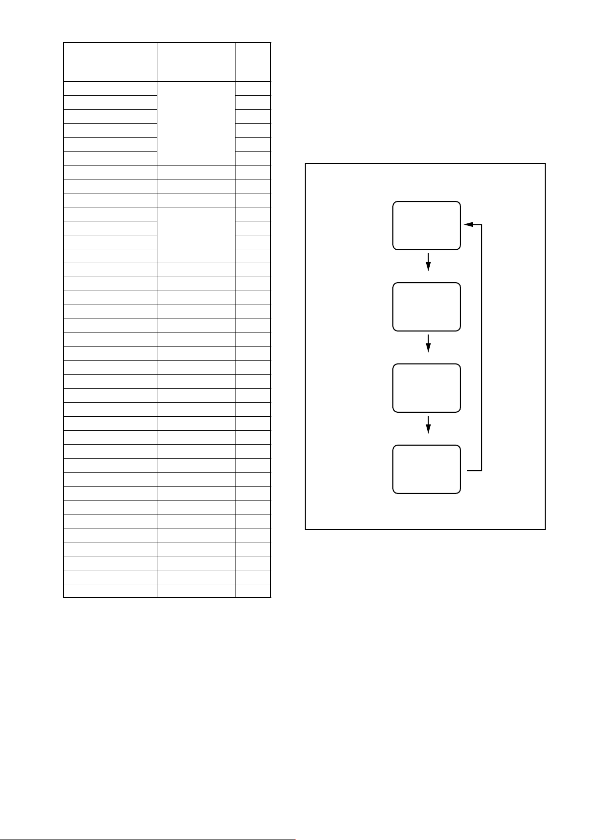
2. Purity Check Mode
This mode cycles through full-screen displays of red,
green, blue, and white to check for non-active pixels.
1. Enter the Service mode.
2. Each time pressing [7] button on the service
remote control unit, the display changes as
follows.
Purity Check Mode
Red mode
[7] button
[7] button
Green mode
[7] button
Blue mode
[7] button
White mode
Note:
When entering this mode, the default setting is White mode.
NOTE: * These data value will be changed by the White
Balance Adjustment.
6-2 L5920EA
Page 19
3. Flicker Adjustment
4. Auto Calibration
*This adjustment is needed when reparing T-CON
CBA.
1. Enter the Service mode.
2. Press [2] button on the remote control unit.
The following screen appears.
3. If Flicker Adjustment is not fit, the screen become
the following.
Purpose: To bring the color adjustment of each
component into standard alignment.
Symptom of Misadjustment: If this adjustment is
incorrect, component signals do not reproduce the
corresponding color.
Gain Adjustment
1. Input white raster signal (5%=5 IRE, 100%=100
IRE) from Component jack.
INPUT SIGNAL
5%=5IRE
2. Enter the service mode.
3. To enter the Auto Calibration adjustment mode,
press [5] button on the service remote control unit.
4. To start auto adjustment, press [CH o] button on
the service remote control unit.
- In the auto adjustment mode, “Please Wait”
appears on the screen.
- Upon completion, “OK” and appears on the
screen.
- If the auto adjustment failure, “ NG” appears on
the screen.
100%=100IRE
FLASH (Go and Off)
4. Turn the VR1 on the LCD Module so that flash
stops.
Offset Adjustment
5. Input white raster signal (5%=5 IRE) from
Component jack.
INPUT SIGNAL
5%=5IRE
6. Enter the service mode.
7. To enter the Auto Calibration adjustment mode,
press [6] button on the service remote control unit.
8. To start auto adjustment, press [CH o] button on
the service remote control unit.
- In the auto adjustment mode, “Please Wait”
appears on the screen.
- Upon completion, “OK” and appears on the
screen.
- If the auto adjustment failure, “ NG” appears on
the screen.
6-3 L5920EA
Page 20
The following adjustment normally are not
attempted in the field. Only when replacing the
LCD Panel then adjust as a preparation.
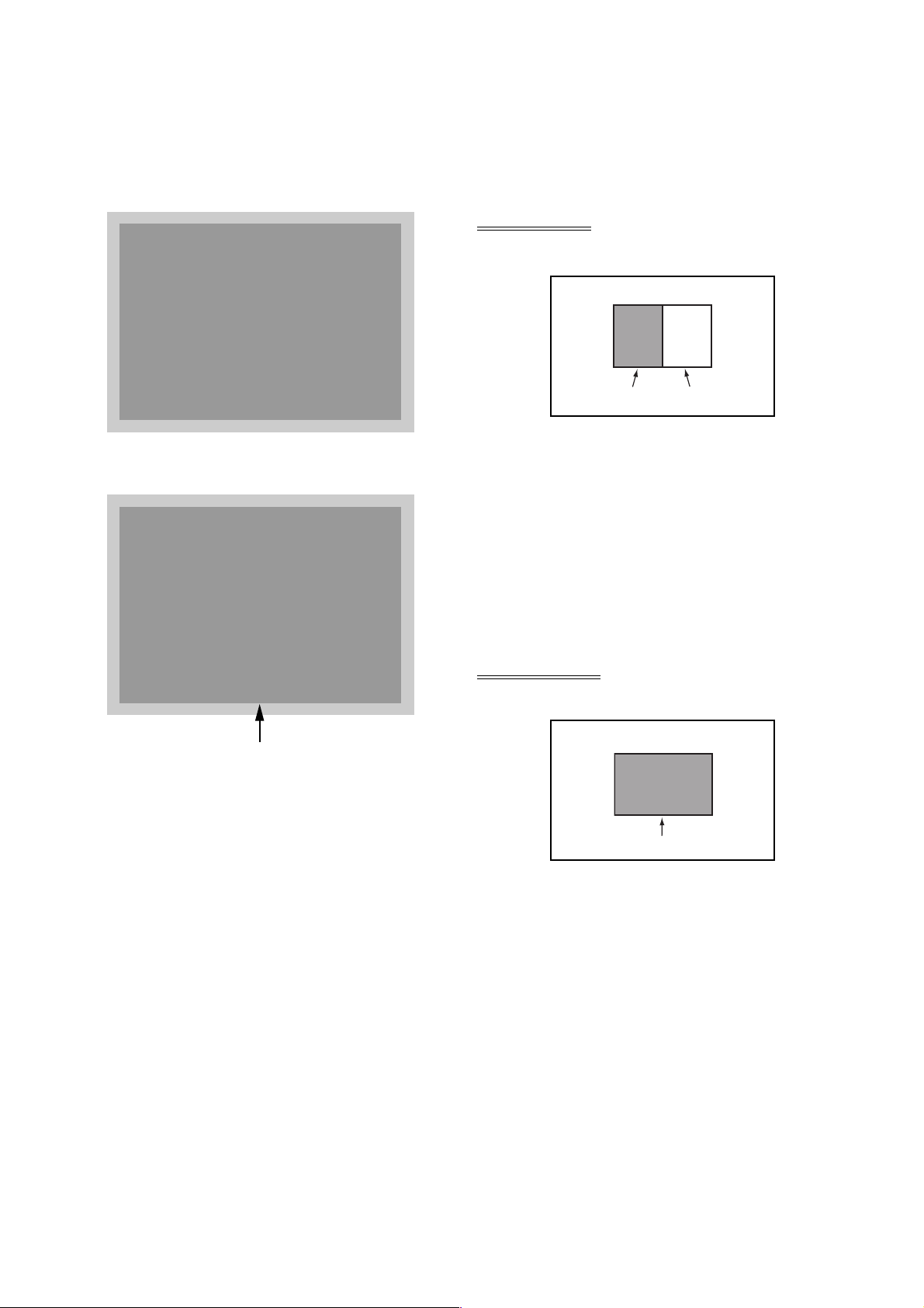
5. White Balance Adjustment
*This adjustment is needed when reparing T-CON
CBA.
Purpose: To mix red, green and blue beams correctly
for pure white.
Symptom of Misadjustment: White becomes bluish
or reddish.
Test Point Adj. Point Mode Input
[CVBS]
C/D/S 1
Screen
Pattern Generator,
Color analyzer
INPUT: WHITE 70%,25%
1. Operate the unit for more than 20 minutes.
2. Input the White Purity.
3. Set the color analyzer to the CHROMA mode and
bring the optical receptor to the center on the
LCD-Panel surface after zero point calibration as
shown above.
Note: The optical receptor must be set
perpendicularly to the LCD Panel surface.
4. [CVBS]
Enter the Service mode. Press “VOL p” button on
the remote control unit and select “C/D/S 1” mode.
VOL. p
buttons
M. EQ. Spec.
L = 50 cm
[YUV]
C/D/S 2
[RGB]
C/D/S 3
(APL 70%)
x: 0.242 to 0.302,
y: 0.248 to 0.308
(APL 25%)
x: 0.262 to 0.282,
y: 0.268 to 0.288
Figure
It carries out in a darkroom.
Perpendicularity
Color Analyzer
INPUT SIGNAL
25%=25IRE70%=70IRE
White Purity
(APL 70%)
or
(APL 25%)
[YUV]
Enter the Service mode. Press “VOL p” button on
the remote control unit and select “C/D/S 2” mode.
[RGB]
Enter the Service mode. Press “VOL p” button on
the remote control unit and select “C/D/S 3” mode.
5. [CVBS]----(APL 70%)
Press “6” button to select “DB 1(C/D/S 1)” for Blue
adjustment. Press “4” button to select “DR 1(C/D/S
1)” for Red adjustment. When “x” value and “y”
value are not within specification, adjust “DB 1(C/
D/S 1)” or “DR 1(C/D/S 1)”. Refer to “1. Initial
Setting.”
[CVBS]----(APL 25%)
Press “3” button to select “COB 1(C/D/S 1)” for
Blue adjustment. Press “1” button to select “COR
1(C/D/S 1)” for Red adjustment. When “x” value
and “y” value are not within specification, adjust
“COB 1(C/D/S 1)” or “COR 1(C/D/S 1)”. Refer to
“1. Initial Setting.”
After adjusting (APL 25%), verify (APL 70%) again
and adjust repeatedly until both values are within
specification.
6. [YUV]----(APL 70%)
Press “6” button to select “DB 2(C/D/S 2)” for Blue
adjustment. Press “4” button to select “DR 2(C/D/S
2)” for Red adjustment.When “x” value and “y”
value are not within specification, adjust “DB 2(C/
D/S 2)” or “DR 2(C/D/S 2)”. Refer to “1. Initial
Setting.”
[YUV]----(APL 25%)
Press “3” button to select “COB 2(C/D/S 2)” for
Blue adjustment. Press “1” button to select “COR
2(C/D/S 2)” for Red adjustment.When “x” value
and “y” value are not within specification, adjust
“ C O B 2 (C / D / S 2 )” o r “ C O R 2 ( C / D/ S 2 ) ” .
Refer to “1. Initial Setting.”
After adjusting (APL 25%), verify (APL 70%) again
and adjust repeatedly until both values are within
specification.
7. [RGB]----(APL 70%)
Press “6” button to select “DB 3(C/D/S 3)” for Blue
adjustment. Press “4” button to select “DR 3(C/D/S
3)” for Red adjustment.When “x” value and “y”
value are not within specification, adjust “DB 3(C/
D/S 3)” or “DR 3(C/D/S 3)”. Refer to “1. Initial
Setting.”
[RGB]----(APL 25%)
Press “3” button to select “COB 3(C/D/S 3)” for
Blue adjustment. Press “1” button to select “COR
3(C/D/S 3)” for Red adjustment.When “x” value
and “y” value are not within specification, adjust
“ C O B 3 (C / D / S 3 )” o r “ C O R 3 ( C / D/ S 3 ) ” .
Refer to “1. Initial Setting.”
After adjusting (APL 25%), verify (APL 70%) again
and adjust repeatedly until both values are within
specification.
8. Turn the power off and on again. (Main power
button on the TV unit.)
6-4 L5920EA
Page 21

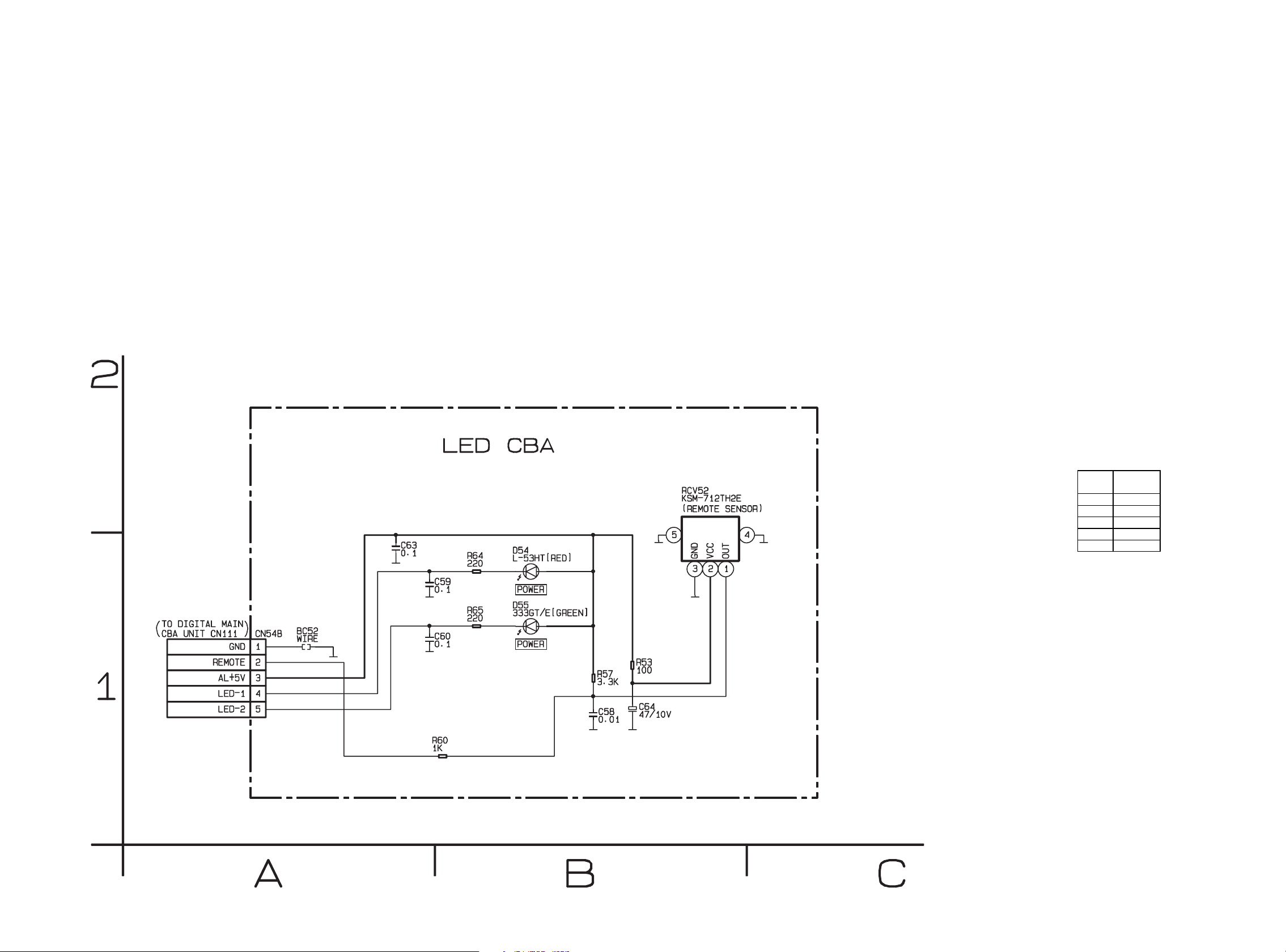
BLOCK DIAGRAMS
System Control Block Diagram
D55D54
LED CBA
REMOTE
SENSOR
RCV52
CN54BCN111
REMOTE82
LED-235
DRIVE
Q462
POWER POWER
LED-144
DRIVE
Q463
CN104ACN104B
TO AUDIO
BLOCK DIAGRAM
SCL
SDA
VOLUME
AUDIO-MUTE
SCL
TO VIDEO SELECTOR
BLOCK DIAGRAM
SDA
TO
INVERTER
BLOCK
BACKLIGHT-SW
BACKLIGHT-ADJ
DRIVE
Q507
CN101ACN101B
DIAGRAM
DRIVE
Q508
P-ON-H1
P-ON-H2
CN102ACN102B
TO POWER SUPPLY
BLOCK DIAGRAM
P-ON-H3
MAIN CBADIGITAL MAIN CBA UNIT
IC101
(TV MICRO CONTROLLER)
17
RTC-IN
KEY-IN1
93
37
LED-251LED-1
AUDIO-MUTE
VOLUME420
SCL14 10
SDA15 9
123
1
77
VOLUME
AUDIO-MUTE
BACKLIGHT-SW
BACKLIGHT-ADJ
13 11
12 12
TO DIGITAL
SIGNAL PROCESS
SDA
SCL
567
282726
SCL
SDA
WP
BUS-OPEN
IC103 (MEMORY)
BLOCK DIAGRAM
SCL
SDA
52
22
BACKLIGHT-SW
BACKLIGHT-ADJ
X100
XIN
11
10MHz
OSC
XOUT
13
P-ON-H118 6
P-ON-H217 7
P-ON-H316 8
56
57
P-ON-H159P-ON-H2
P-ON-H3
IC102
RESET
10
45
RESET
KEY-IN144
CN11B CN11A
KEY SWITCH
FUNCTION CBA
7-1
AL+5V
L5920BLS
Page 22

Video Selector Block Diagram
VIDEO SIGNAL
JK704
(SCART)
WF9
VIDEO-OUT1
VIDEO-OUT2
19
40
40
38
TO DIGITAL
VIDEO-R15
CN104A
343332
SIGNAL PROCESS
VIDEO-G14
VIDEO-B13
(CN104B)
BLOCK DIAGRAM
RGB-SYNC17
36
WF8WF7
WF7
WF1
WF2WF3
VIDEO11
CN103A
S-VIDEO-Y14
28
TO DIGITAL
S-VIDEO-C13
30
SIGNAL PROCESS
BLOCK DIAGRAM
COMPONENT-Y6COMPONENT-Pb8COMPONENT-Pr
(CN103B)
9
WF5 WF6
WF4
VIDEO
INPUT
SELECTOR
I2C
I/F
IC701
(VIDEO SELECTOR)
44
MAIN CBA
45
SDA
SCL
TO SYSTEM CONTROL
BLOCK DIAGRAM
14
16
JK702
17
VIDEO
4
VIDEO-IN3
JK704
(SCART)
24
26
20
41
VIDEO-IN1
VIDEO-IN2
8
6
21
3 4
JK703
YC
S-VIDEO
-IN
JK704
7371692249
11715
(SCART)
B-IN1
G-IN1
R-IN1
322836
B-IN2
G-IN2
47
R-IN2
JK701
COMPONENT
Y-IN
COMPONENT
Pb-IN
COMPONENT
Pr-IN
TU31
(TUNER UNIT)
ANT-IN
(ANALOG)
7-2
L5920BLV
Page 23

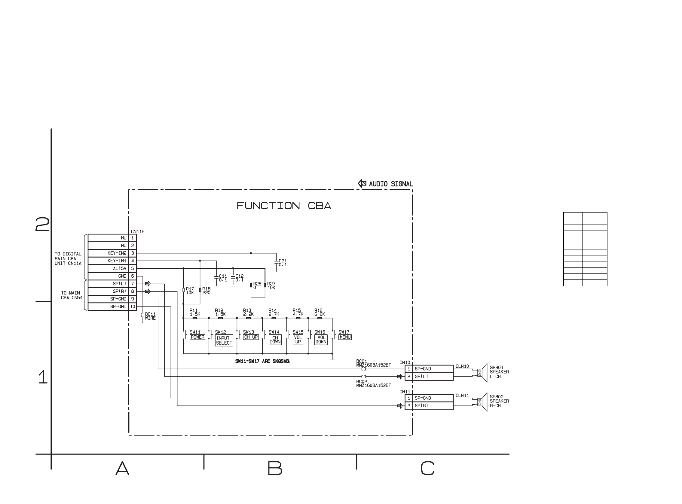
Audio Block Diagram
SP801
SPEAKER
L-CH
SP802
SPEAKER
R-CH
AUDIO SIGNAL
IC801
(AUDIO AMP)
CLN10
SP(L) 2
SP-GND 1
CN11BCN54 CN10
SP(L)47
SP(R)38
AMP
5 7
WF10
1
97
99
CLN11
CN11
SP(R) 2
SP-GND 1
TO SYSTEM
CONTROL
BLOCK DIAGRAM
VOLUME
AUDIO-MUTE
JK704
(SCART)
AUDIO(L)-OUT1
AUDIO(R)-OUT1
AUDIO(L)-OUT2
AUDIO(R)-OUT2
3221
24
AMP
2 12
FUNCTION CBA
VOLUME
CONTROL
MUTE
CONTROL
611
MAIN CBA
96
98
100
IC701
(AUDIO SELECTOR)
L-CH
IC851
(SOUND PROCESSOR)
93
91
8987858179
317 2
30AUDIO 6 43
R-CH
IF SIGNAL
PROCESS
SIF
(L-CH)
AUDIO SW
I2C I/F
(R-CH)
I2C I/F
44
45
13 12
SDA
SCL
JK702
AUDIO SW
94929088868280
JK704
HDMI(L)21 3
HDMI(R)20 4
HDMI-AUDIO(L)
HDMI-AUDIO(R)
23 1
22 2
CN103B CN103A
HDMI(L)
6
2
23
27
(SCART)
JK701
HDMI(R)
DIGITAL MAIN CBA UNIT
TU31
(TUNER UNIT)
TO SYSTEM
CONTROL
BLOCK DIAGRAM
AUDIO(L)-IN3
AUDIO(R)-IN3
AUDIO(R)-IN2
AUDIO(L)-IN2
AUDIO(L)-IN1
AUDIO(R)-IN1
7-3
COMPONENT
AUDIO(L)-IN
AUDIO(R)-IN
COMPONENT
TO DIGITAL
SIGNAL PROCESS
BLOCK DIAGRAM
JK201
HDMI
JK202
AUDIO(L)-IN
HDMI
L5920BLA
AUDIO(R)-IN
Page 24

Digital Signal Process Block Diagram
LCD MODULE
LVDS TX0(+)4
LVDS TX0(-)3
LVDS TX1(+)8
LVDS TX1(-)7
LVDS TX2(+)12
LVDS TX2(-)11
LVDS TX3(+)20
LVDS TX3(-)19
LVDS CLK(+)16
LVDS CLK(-)15
CN400
AUDIO SIGNAL
VIDEO SIGNAL
IC333 (SCALER) IC400 (LVDS TRANSMITTER)
33
A/D
ANALOG
442113
CONVERTER
SW
404231
R DATA
133
49
(0-7)
135
~
56
139
75
143~~106
DIGITAL
SIGNAL
191
196
R DATA
(0-7)
12
74
7776818085
202326
G DATA
113
PROCESS
(SCALER)
200
201~202
19
(0-7)
LVDS
116
TX
119
84
~
29~~374245
B DATA
(0-7)
~~
121~~122
123
206
208
210~~211
G DATA
(0-7)
2
9
127
46
132
~~
B DATA
(0-7)
92
214
2
99
HDVDEN
60
61
89
90
VD
5
62
88
EN
HDHDVD
7
87
HD
83
PLL
59
105
CLK
6
85VD89
82
CLK
190
CLK
82
I2C
I2C I/F
83
I/F
Q401Q400
66 69
SDA
SCL
TO SYSTEM CONTROL
BLOCK DIAGRAM
TO AUDIO
BLOCK DIAGRAM
HDMI(L)
HDMI(R)
DIGITAL MAIN CBA UNIT
L-CH
R-CH
VIDEO-R
CN104B
9
TO VIDEO
VIDEO-G
VIDEO-B
10
11
(CN104A)
SELECTOR
BLOCK DIAGRAM
RGB-SYNC
7
IC201 (HDMI INTERFACE)
CN103B
746879
VIDEO
S-VIDEO-Y
S-VIDEO-C
COMPONENT-Y
1310111816
TO VIDEO
SELECTOR
BLOCK DIAGRAM
CLAMP A/D
MUX
COMPONENT-Pb
COMPONENT-Pr
15
(CN103A)
MUX MATRIX
HDMI
35343837414043
JK200
79461
DATA 0(-)
DATA 1(-)
DATA 0(+)
DATA 1(+)
RECEIVER
3
101216
DATA 2(-)
DATA 2(+)
CLOCK(+)
-IN
HDMI
44
15
CLOCK(-)
DDCDATA
DDCCLOCK
IC100
(AUDIO D/A CONVERTER)
AUDIO
D/A
CONVERTER
7
8 15146
5
2223272120
AUDIO
DECODER
Q209
I2C
I/F
SDA
SCL
IC200 (HDMI MEMORY)
5
50
49
Q210
6
7-4
L5920BLLCD
Page 25

Inverter Block Diagram
BACK
LIGHT
BACK
LIGHT
BACK
LIGHT
BACK
LIGHT
BACK
LIGHT
BACK
LIGHT
LCD MODULE
1
2
CN1050
9
T1050
3
4
DRIVE
Q1102,Q1103
1
2
CN1100
Q1020
8
7
9
10
5
2
T1100
6
1
10
2
3
4
DRIVE
Q1100,Q1101
8
5
1
1
2
CN1150
7
9
8
10
T1150
6
5
2
3
1
4
7
6
1
CN1200
9
T1200
3
Q1252,Q1253
2
10
2
4
DRIVE
1
2
CN1250
8
7
9
8
10
5
T1250
6
1
2
3
4
DRIVE
Q1250,Q1251
5
1
1
2
CN1300
7
9
8
7
10
T1300
6
5
6
2
3
1
4
INVERTER CBAMAIN CBA
CN1000CN703
LDR2
HDR2
INV+24V1-8 13-20
BACKLIGHT-ADJ
19 2
INV+24V
BACKLIGHT-ADJ
TO SYSTEM CONTROL
BLOCK DIAGRAM
BACKLIGHT-SW
20 1
BACKLIGHT-SW
PROTECT-3
18 3
TO POWER SUPPLY
Q1000
PROTECT-3
BLOCK DIAGRAM
+5V
REG.
LDR1
HDR1
6
DRIVE
LOGIC
IC1001 (DRIVER)
12
15
SW
CTL
IC1000 (INVERTER CONTROL)
4
11
DRIVE
OUTPUT
DRIVE
LF OSC
10
CONTROL
10
3
DRIVE
LOGIC
14
DRIVE
LOGIC
13
1
15
IGNITION
5
1
VDD
13
HF OSC
/PROTECTION
CONTROL
LOGIC
8
VDD
LDR2
4
VCC
Q1002
213
HDR2
V-REF
13
12910
14
Q1003
V-REF
8
Q1001
6
5
7
V-REF
213
4
VCC
IC1550 (COMPARATOR)
13
12910
14
VS
IS
6
5
8
7
LDR1
HDR1
IC1500 (COMPARATOR)
6
7-5
L5920BLINV
Page 26

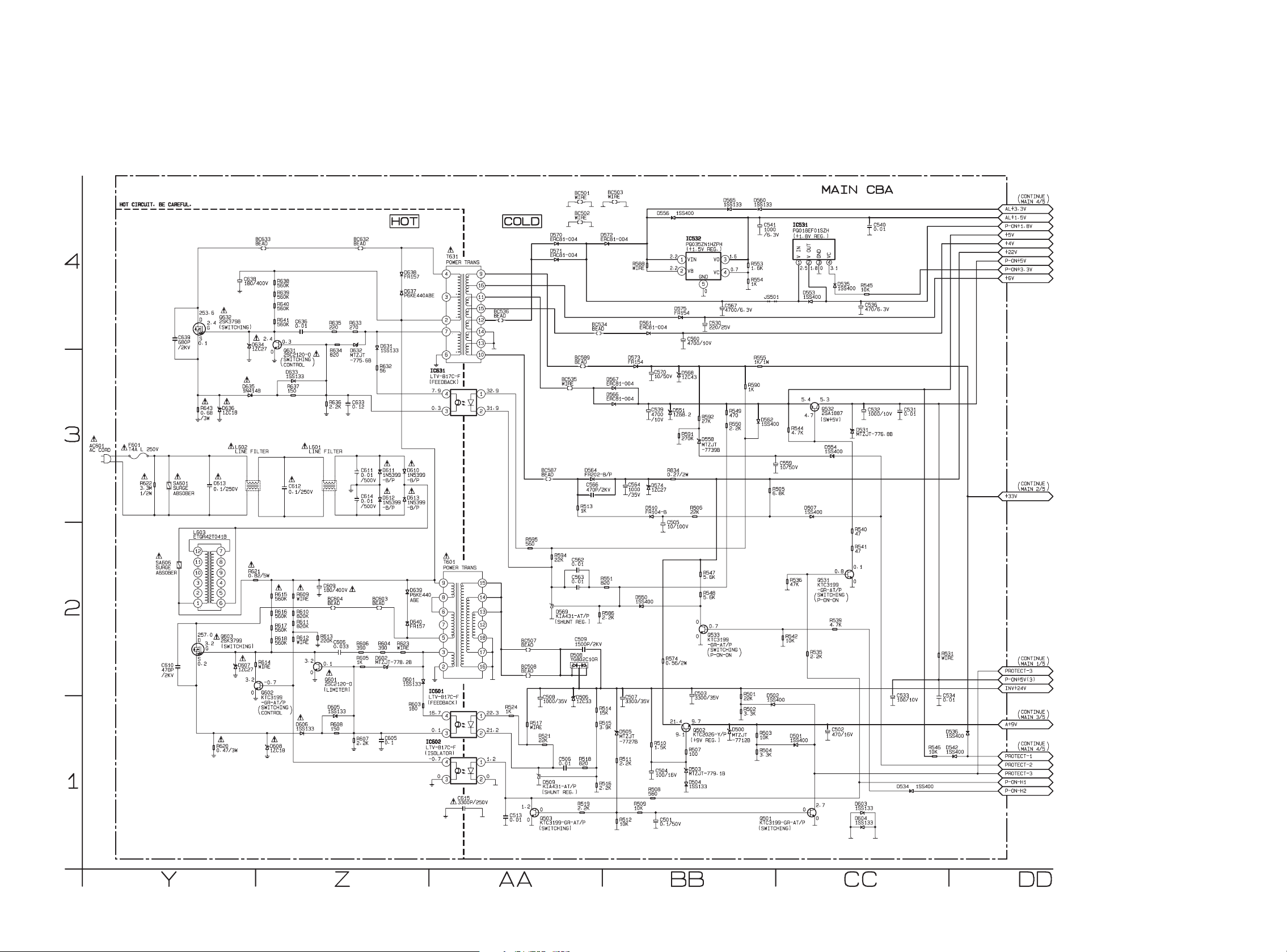
Power Supply Block Diagram
NOTE:
The voltage for parts in hot circuit is measured using
hot GND as a common terminal.
CAUTION !
For continued protection against fire hazard,
replace only with the same type fuse.
P-ON+5V
+33V
CONTROL
BLOCK DIAGRAM
P-ON-H3
Q503
P-ON+5V(2)
+5V REG.
IC516
1 2
TO INVERTER
BLOCK DIAGRAM
PROTECT-3
4
Q534
Q532
SW +5V
Q531
INV+24V
TO SYSTEM
P-ON-H2
P-ON-H1
MAIN CBA
AL+3.3V
+3.3V REG.
IC513
1 2
+3.3V
+3.3V REG.
IC514
1 2
Q510
4
P-ON+3.3V
SW +3.3V
Q512
P-ON+1.8V
+1.8V REG.
IC531
1 2
AL+1.5V
AL+9V
+9V REG.
Q502
4
+1.5V REG.
IC532
1 3
+5V REG.
IC515
1 3
Q533
P-ON+12V
+22V
SW +22V
Q804,Q805,Q806
AL+5V
Q801
REG.
SHUNT
D509
16
18
13
14
15
T601
8
9
Q603
HOT COLD
L603
BRIDGE
RECTIFIER
D610 - D613
LINE
FILTER
L601
LINE
FILTER
L602
CAUTION !
Fixed voltage (or Auto voltage selectable) power supply circuit is used in this unit.
If Main Fuse (F601) is blown , check to see that all components in the power supply
circuit are not defective before you connect the AC plug to the AC power supply.
Otherwise it may cause some components in the power supply circuit to fail.
HOT CIRCUIT. BE CAREFUL.
F601
T4A L 125V
SW
17
6
5
3
2
14
IC601
(FEEDBACK)
Q601
IC602
3 2
LIMITER
1
4
(ISOLATOR)
Q602
SW-CLT
REG.
SHUNT
IC631
(FEEDBACK)
14
D569
Q631
3 2
SW-CTL
9
T631
Q632
16
4
SW
2
3
15
11
3
14
12
2
7
10
13
6
AC601
AC CORD
7-6
L5920BLP
Page 27
SCHEMATIC DIAGRAMS / CBA'S AND TEST POINTS
Standard Notes
Many electrical and mechanical parts in this chassis have special characteristics. These characteristics often
pass unnoticed and the protection afforded by them cannot necessarily be obtained by using replacement
components rated for higher voltage, wattage, etc. Replacement parts that have these special safety
characteristics are identified in this manual and its supplements; electrical components having such features are
identified by the mark “!” in the schematic diagram and the parts list. Before replacing any of these components,
read the parts list in this manual carefully. The use of substitute replacement parts that do not have the same
safety characteristics as specified in the parts list may create shock, fire, or other hazards.
Notes:
1. Do not use the part number shown on these drawings for ordering. The correct part number is shown in the
parts list, and may be slightly different or amended since these drawings were prepared.
2. All resistance values are indicated in ohms (K = 10
3. Resistor wattages are 1/4W or 1/6W unless otherwise specified.
4. All capacitance values are indicated in µF (P = 10
5. All voltages are DC voltages unless otherwise specified.
Note of Capacitors:
ML --- Mylar Cap. PP --- Metallized Film Cap. SC --- Semiconductor Cap. L --- Low Leakage type
Temperature Characteristics of Capacitors are noted with the following:
B --- ±10% CH --- 0±60 ppm/°C CSL --- +350~-1000 ppm/°C
3
, M = 106).
-6
µF).
Tolerance of Capacitors are noted with the following:
Z --- +80~-20%
Note of Resistors:
CEM --- Cement Res. MTL --- Metal Res. F --- Fuse Res.
Capacitors and transistors are represented by the following symbols.
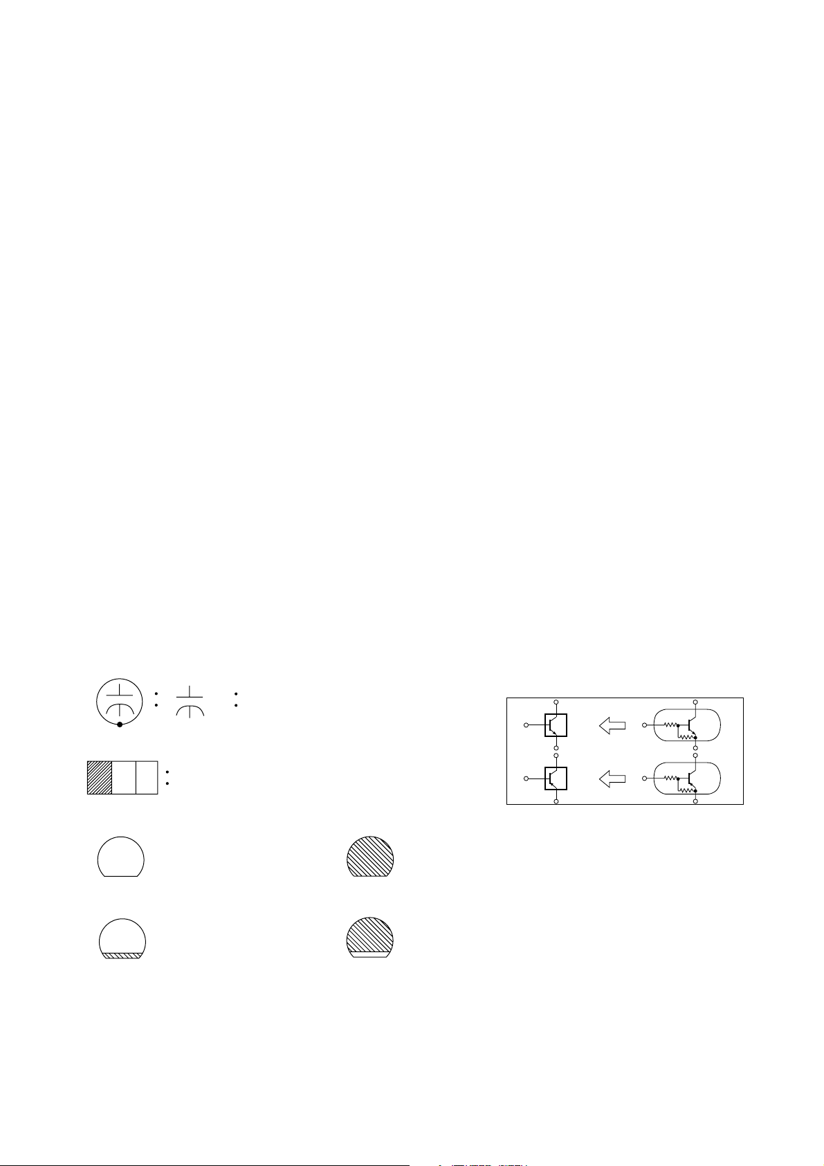
CBA Symbols
(Top View) (Bottom View)
+
Electrolytic Capacitor
(Bottom View)
Transistor or Digital Transistor
E C B
(Top View)
NPN Transistor
E C B
(Top View)
(Top View)
PNP Transistor
E C B
(Top View)
Schematic Diagram Symbols
Digital Transistor
E C B
NPN Digital Transistor
PNP Digital Transistor
E C B
8-1 LC4P_SC
Page 28

LIST OF CAUTION, NOTES, AND SYMBOLS USED IN THE SCHEMATIC DIAGRAMS ON
THE FOLLOWING PAGES:
1. CAUTION:
FOR CONTINUED PROTECTION AGAINST FIRE HAZARD, REPLACE ONLY WITH THE SAME TYPE
FUSE.
2. CAUTION:
Fixed Voltage (or Auto voltage selectable) power supply circuit is used in this unit.
If Main Fuse (F601) is blown, first check to see that all components in the power supply circuit are not
defective before you connect the AC plug to the AC power supply. Otherwise it may cause some components
in the power supply circuit to fail.
3. Note:
1. Do not use the part number shown on the drawings for ordering. The correct part number is shown in the
parts list, and may be slightly different or amended since the drawings were prepared.
2. To maintain original function and reliability of repaired units, use only original replacement parts which are
listed with their part numbers in the parts list section of the service manual.
4. Voltage indications on the schematics are as shown below:
Plug the TV power cord into a standard AC outlet.:
2
(Unit: Volt)
1
5.0 5.0
3
Power on mode
5. How to read converged lines
1-D3
Distinction Area
Line Number
(1 to 3 digits)
Examples:
1. "1-D3" means that line number "1" goes to the line number
"1" of the area "D3".
2. "1-B1" means that line number "1" goes to the line number
"1" of the area "B1".
6. Test Point Information
: Indicates a test point with a jumper wire across a hole in the PCB.
: Used to indicate a test point with a component lead on foil side.
: Used to indicate a test point with no test pin.
: Used to indicate a test point with a test pin.
Voltage
Indicates that the voltage
is not consistent here.
3
2
1
AREA D3
1-B1
AREA B1
1-D3
ABCD
8-2 LC4P_SC
Page 29

Main 1/5 Schematic Diagram
NOTE:
# is an unnecessary part of the circuit configuration;
therefore servicing is not required, for this product operates independently of this part.
8-3
L5920SCM1
Page 30

Main 2/5 Schematic Diagram
NOTE:
# is an unnecessary part of the circuit configuration;
therefore servicing is not required, for this product operates independently of this part.
8-4
L5920SCM2
Page 31

Main 3/5 Schematic Diagram
CN103A
14.6
24.6
32.5
42.5
50
63.8
70
80
90
10 0
11 2.4
12 0
13 2.5
14 2.4
15 0
16 --17 --18 --19 --20 --21 5.0
22 5.0
23 ---
VOLTAGE CHART
Pin No. Voltage
8-5 L5920SCM3
Page 32

Main 4/5 Schematic Diagram
CN101A CN104A
10 10
21.8 2 ---
30 3---
43.3 4 ---
50 5---
65.0 6 ---
70 70
80 82.5
95.3 94.8
10 5.3 10 4.9
11 3.3 11 0
12 5.0 12 2.7
13 0 13 2.4
14 --- 14 2.4
15 --- 15 2.4
16 --- 16 0
17 --- 17 2.4
18 --- 18 0
19 --- 19 --20 --- 20 1.4
21 --- 21 0
22 --- 22 --23 --- 23 3.3
CN102A
10
2 --30
4 --50
62.7
73.2
80
9 --10 0.2
11 3.7
12 -0.6
13 0
14 5.0
15 0
16 0
17 3.3
18 3.3
19 0
20 1.6
21 0
22 3.3
23 0
Pin No. Voltage
Pin No. Voltage
Pin No. Voltage
NOTE:
# is an unnecessary part of the circuit configuration;
therefore servicing is not required, for this product operates independently of this part.
VOLTAGE CHART
8-6
L5920SCM4
Page 33
Main 5/5 Schematic Diagram
CAUTION !
Fixed voltage (or Auto voltage selectable) power supply circuit is used in this unit.
If Main Fuse (F601) is blown , check to see that all components in the power supply
circuit are not defective before you connect the AC plug to the AC power supply.
Otherwise it may cause some components in the power supply circuit to fail.
CAUTION !
For continued protection against fire hazard,
replace only with the same type fuse.
NOTE:
The voltage for parts in hot circuit is measured using
hot GND as a common terminal.
8-7
L5920SCM5
Page 34
Function Schematic Diagram
VOLTAGE CHART
CN11B
Pin No. Voltage
1--2---
35.0
45.0
55.0
60
75.2
85.2
90
10 0
8-8
L5920SCF
Page 35
LED Schematic Diagram
VOLTAGE CHART
CN54B
Pin No. Voltage
10
25.0
35.0
43.5
50.1
8-9
L5920SCL
Page 36

Inverter Schematic Diagram
8-10
L5920SCINV
Page 37

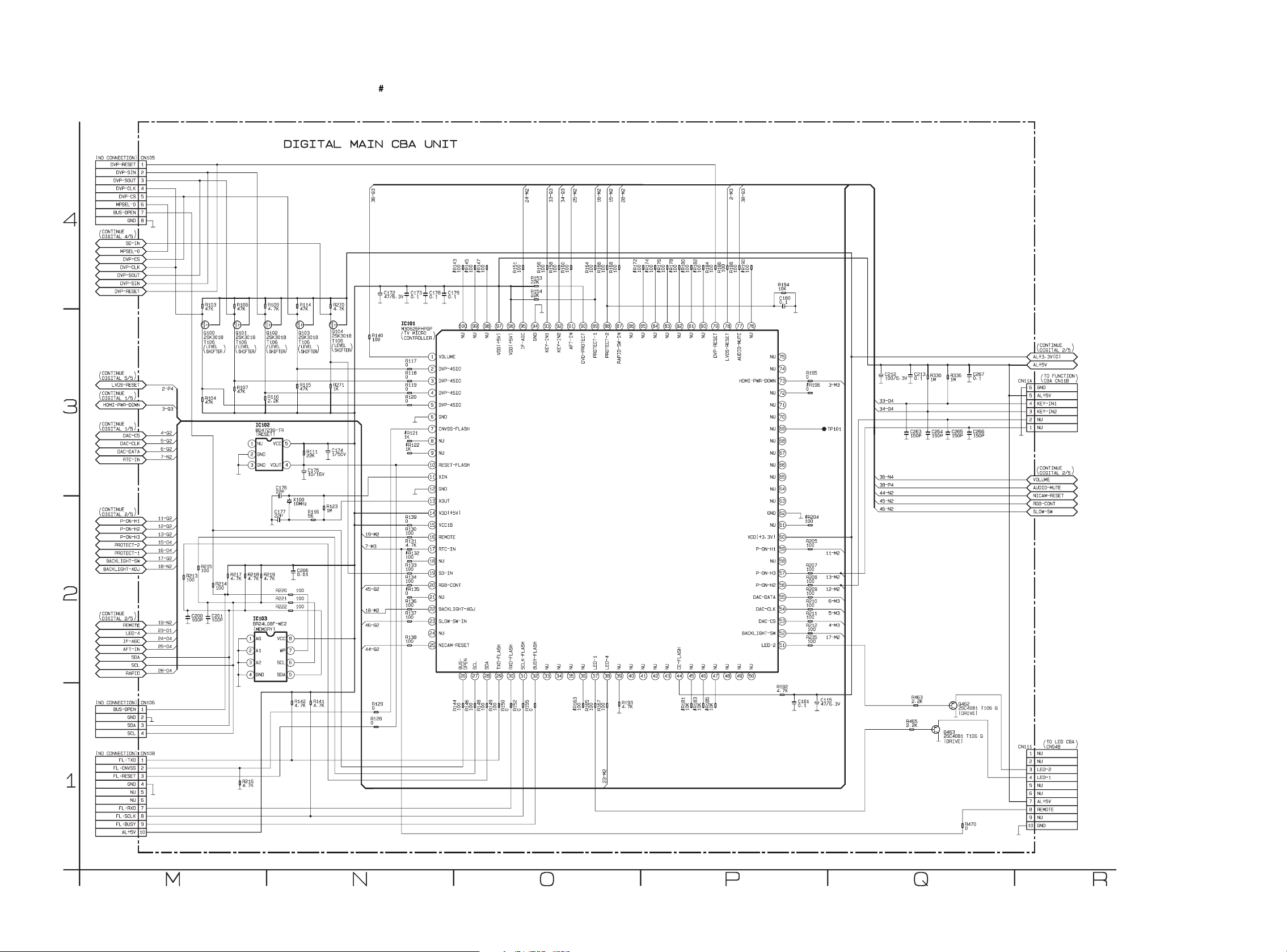
Digital Main 1/5 Schematic Diagram
NOTE:
# is an unnecessary part of the circuit configuration;
therefore servicing is not required, for this product operates independently of this part.
8-11
L5920SCD1
Page 38

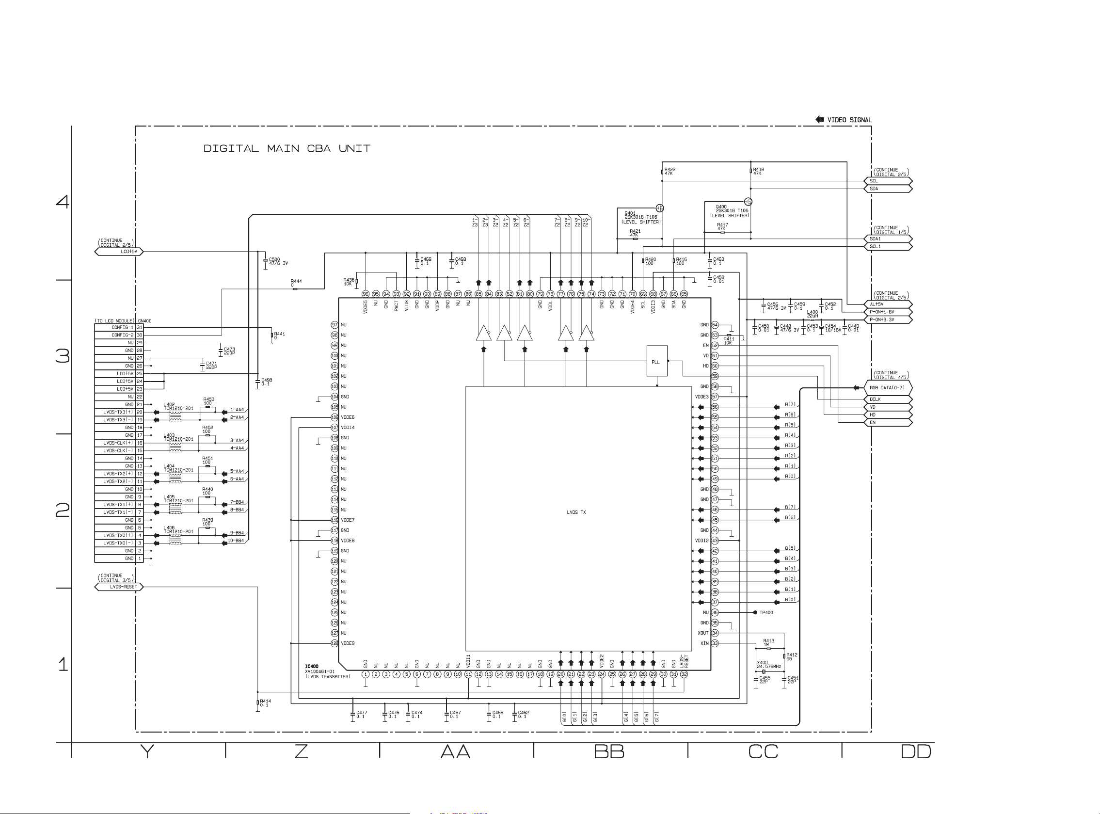
Digital Main 2/5 Schematic Diagram
8-12
L5920SCD2
Page 39
Digital Main 3/5 Schematic Diagram
NOTE:
# is an unnecessary part of the circuit configuration;
therefore servicing is not required, for this product operates independently of this part.
8-13
L5920SCD3
Page 40

Digital Main 4/5 Schematic Diagram
8-14
L5920SCD4
Page 41
Digital Main 5/5 Schematic Diagram
8-15
L5920SCD5
Page 42

Main CBA Top View
Because a hot chassis ground is present in the power
supply circut, an isolation transformer must be used.
Also, in order to have the ability to increase the input
slowly, when troubleshooting this type power supply
circuit, a variable isolation transformer is required.
CAUTION !
For continued protection against fire hazard,
replace only with the same type fuse.
NOTE:
The voltage for parts in hot circuit is measured using
hot GND as a common terminal.
CAUTION !
Fixed voltage (or Auto voltage selectable) power supply circuit is used in this unit.
If Main Fuse (F601) is blown , check to see that all components in the power supply
circuit are not defective before you connect the AC plug to the AC power supply.
Otherwise it may cause some components in the power supply circuit to fail.
8-16
BL5820F01011-1
Page 43
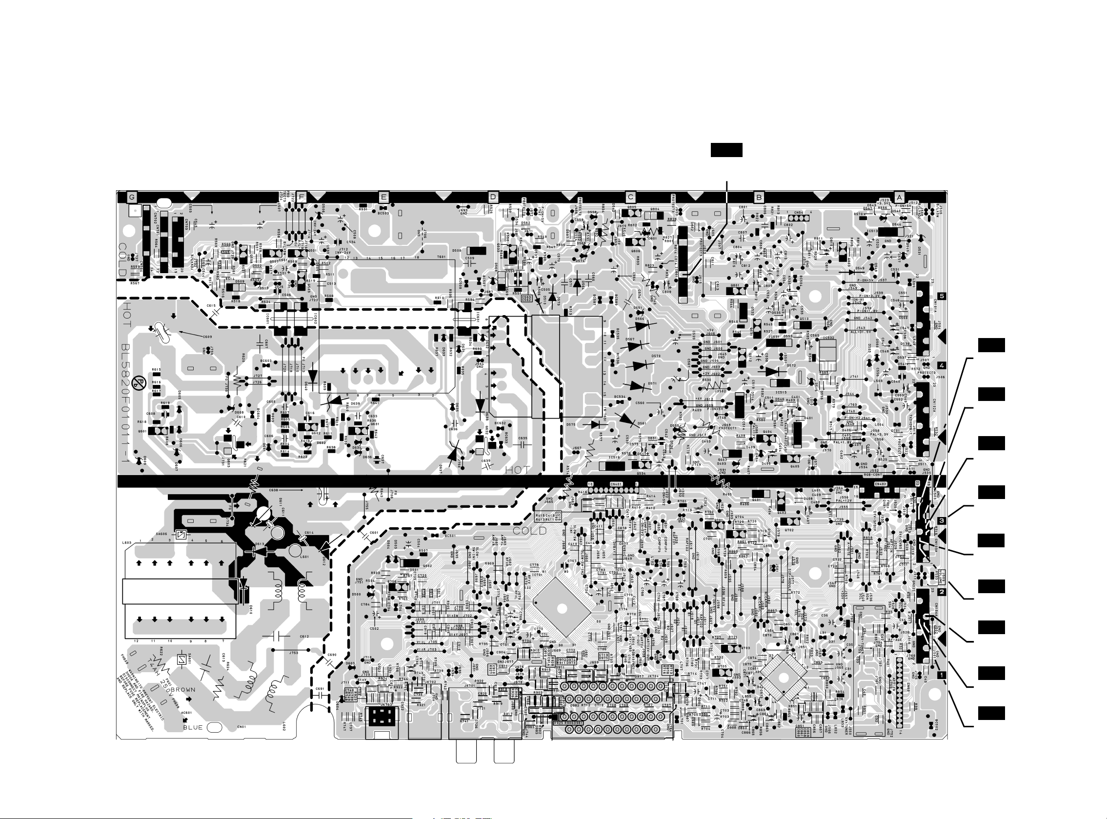
Main CBA Bottom View
CAUTION !
For continued protection against fire hazard,
replace only with the same type fuse.
NOTE:
The voltage for parts in hot circuit is measured using
hot GND as a common terminal.
CAUTION !
Fixed voltage (or Auto voltage selectable) power supply circuit is used in this unit.
If Main Fuse (F601) is blown , check to see that all components in the power supply
circuit are not defective before you connect the AC plug to the AC power supply.
Otherwise it may cause some components in the power supply circuit to fail.
Because a hot chassis ground is present in the power
supply circut, an isolation transformer must be used.
Also, in order to have the ability to increase the input
slowly, when troubleshooting this type power supply
circuit, a variable isolation transformer is required.
WF10
PIN 5OF
IC801
WF2
PIN 14 OF
CN103A
WF3
PIN 13 OF
CN103A
WF1
PIN 11 OF
CN103A
WF6
PIN 9 OF
CN103A
WF5
PIN 8 OF
CN103A
WF4
PIN 6 OF
CN103A
WF9
PIN 15 OF
CN104A
WF7
PIN 13 OF
CN104A
WF8
PIN 14 OF
CN104A
8-17
BL5820F01011-1
Page 44

Function CBA Top View
LED CBA Top View
Function CBA Bottom View
BL5820F01011-2
LED CBA Bottom View
BL5820F01011-3
8-18
Page 45

Inverter CBA Top View
8-19
BL4400F01022
Page 46

Inverter CBA Bottom View
8-20
BL4400F01022
Page 47

WAVEFORMS
WF1 ~ WF6 = Waveforms to be observed at
Waveform check points.
(Shown in Schematic Diagram.)
Input: PAL Color Bar Signal (with 1kHz Audio Signal)
WF1
WF2
Pin 11 of CN103A
CVBS 0.2V 20µs
Pin 14 of CN103A
WF4
WF5
Pin 6 of CN103A
COMPONENT-Y 0.2V 20µs
Pin 8 of CN103A
20
µ
s
S-VIDEO-Y 0.2V
WF3
Pin 13 of CN103A
S-VIDEO-C 0.2V
20µs
20µs
COMPONENT-Pb 0.2V 20µs
WF6
Pin 9 of CN103A
COMPONENT-Pr 0.2V 20µs
9-1
L5820WF
Page 48
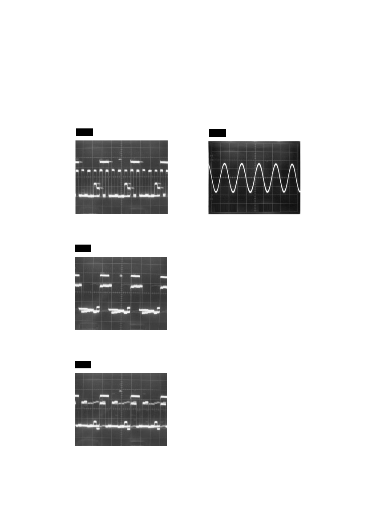
WF7 ~ WF10 = Waveforms to be observed at
Waveform check points.
(Shown in Schematic Diagram.)
Input: PAL Color Bar Signal (with 1kHz Audio Signal)
WF7
WF8
Pin 13 of CN104A
B 0.5V
Pin 14 of CN104A
20µs
WF10
Pin 5 of IC801
AUDIO 0.5V 0.5ms
G 0.5V
WF9
R 0.5V
Pin 15 of CN104A
µ
s
20
µ
s
20
9-2
L5820WF
Page 49

CN111CN54B
10
783
4
LVDS-TX0(-)
GND
GND
1325476
CN400
NU
1
WIRING DIAGRAMS
LCD
MODULE
LVDS-TX2(-)
GND
GND
LVDS-TX1(+)
LVDS-TX1(-)
GND
GND
LVDS-TX0(+)
KEY-IN1
KEY-IN2
NU
354
2
8
AL+5V
LVDS-TX2(+)
GND
GND
LVDS-CLK(-)
LVDS-CLK(+)
GND
9
10131211141517161918212022
GND
6
GND
LVDS-TX3(-)
LVDS-TX3(+)
GNDNULCD+5V
LCD+5V
LCD+5V
GNDNUGNDNUCONFIG-2
23
25242726292830
CONFIG-1
31
GND
13254
DIGITAL MAIN CBA UNITMAIN CBA
1325476
NU
NU
NU
CN101B
CN103B
232122192017181615
REMOTE
NU
LED-1
AL+5V
LED CBA
NU
NU
LED-2
3
2
1
NU
NU
CN11B CN11A
KEY-IN2
FUNCTION CBA
CN10
SP-GND
SP(L)
1
2
CLN10
SP801
SPEAKER
L-CH
8
9
10131211141517161918212022
NU
NU
NU
NU
GND
BACKLIGHT-SW
BACKLIGHT-ADJ
1411121310
LCD+5V
LCD+5V
9785634
KEY-IN1
GND
546
AL+5V
CN11
GND
P-ON+5V
798
GND
SP(L)
SP-GND
1
CLN11
SP802
SPEAKER
GND
SP(R)
SP-GND
SP(R)
2
R-CH
GND
P-ON+3.3V
P-ON+1.8V
2
10
SP-GND
1325476
23
GND
GND
CN102B
AL+3.3V(A)
1
CN104B
232122192017181615
GND
GND
AL+1.5V
8
GND
AL+3.3V(D)
AL+3.3V(D)
HDMI-IN
HDMI
AUDIO(L)-IN
HDMI
AUDIO(R)-IN
CN1000
INV+24V
INV+24V
201819161714151312
9
10131211141517161918212022
GND
GND
AL+5V
1411121310
INV+24V
INV+24V
FBIN
PROTECT-1
INV+24V
INV+24V
NU
PROTECT-2
9785634
INV+24V
INV+24V
P-ON-H3
P-ON-H2
GND
GND
11910 GND
GNDNUGNDNUGND
P-ON-H1
GND
8 GND
2
7 GND
23
1
6 GND
5 GND
4 GND
3 PROTECT-3
BACKLIGHT-ADJ1BACKLIGHT-SW
2
INVERTER CBA
HDMI-AUDIO(R)
HDMI-AUDIO(L)
1325476
CN103A
CN101A
P-ON+1.8V
GND
1325476
TU31
TUNER UNIT
HDMI(R)
HDMI(L)
P-ON+3.3V
GND
GND
COMPONENT-Y
GND
GND
P-ON+5V
GND
SCART JACK
(AV1/AV2)
VIDEO
GND
COMPONENT-Pr
COMPONENT-Pb
8
GND
8
GND
S-VIDEO-C
S-VIDEO-Y
9
10131211141517161918212022
BACKLIGHT-SW
LCD+5V
LCD+5V
9
10131211141517161918212022
GNDNUNUNUNUNUNICAM-RESET
BACKLIGHT-ADJ
GNDNUNUNUNUNUNU
VIDEO
S-VIDEO
-IN3
IN
NU
AUDIO(L)
-IN3
RGB-CONT
NU
23
NUNUNU
23
AUDIO(R)
-IN3
GND
REMOTE(NU)
1325476
CN104A
CN102A
NU
GND
1325476
1325476
CN703
INV+24V
INV+24V
INV+24V
COMPONENT
Y-IN
10-1
NU
NU
NU
LED-4(NU)
P-ON-H1
GND
NU
GND
INV+24V
INV+24V
INV+24V
INV+24V
COMPONENT
Pb-IN
COMPONENT
IF-AGC
P-ON-H2
8
INV+24V
Pr-IN
8
P-ON-H3
8
9
GND
RAPID
VIDEO-B
9
10131211141517161918212022
PROTECT-2
NU
9
10131211141517161918212022
101211GND
GND
COMPONENT
AUDIO(L)
-IN
VIDEO-G
PROTECT-1
FBIN
GND
AL+5V
13GND
14GND
15GND
GND
COMPONENT
AUDIO(R)
-IN
GND
SCL
SDA
AFT-IN
VIDEO-R
GND
RGB-SYNC
GND
GND
AL+3.3V(D)
16GND
17GND
18PROTECT-3
GNDNUVOLUME
AL+3.3V(D)
GND
AL+1.5V
19
20
BACKLIGHT-SW
BACKLIGHT-ADJ
AC CORD
AC601
GNDNUAUDIO-MUTE
23
CN54
GND
AL+3.3V(A)
GND
23
4
SP(L)
2
3
SP(R)
SP-GND
1
SP-GND
L5920WI
Page 50
Cabinet
EXPLODED VIEWS
CLN11
LED CBA
L5
B25
A1
A5
SP801
CLN10
L5
LCD Module Assembly
B1
B25
B13
L1
B13
L5
L5
B13
L1
L5
SP802
L5
B13
B13
L1
L1
B13
L5
L5
L8
L5
L1
B1
L1
L1
T-CON CBA
L5
L5
B21
L3
B2
B14
B13
L8
L3
Function CBA
Inverter CBA
Main CBA
L5
B20
L3
B16
L3
B23
L4
L5
A4
L3
A3
A7
L5
B9
L4
B24
L2
B10
L4
L2
L2
AC601
B13
B31
L8
L5
L2
B16
B28
L2
L5
L8
L8
B30
L6
L2
L2
A6
L6
L6
A18
A26
A24
L2
L2
L2
L2
S5
See Electrical Parts List
for parts with this mark.
Digital Main CBA Unit
B4
L8
L8
B4
L8
L10
A25
L13
A25
L13
L10
L10
B5
L3
L9
L3
L3
L3
L9
11-1 L5920CEX
B3
L3
B6
Page 51

Packing
[ A ]
X2-1,
X2-2,
X2-3,
X2-4,
X2-5,
X2-6,
X2-7,
X2-8
[ B ]
X2-1
X1
[ C ]
X2-2,
X2-4,
X2-7
Tape
[ D ]
X2-1,
X2-7,
X2-9,
X2-10,
X2-11,
X2-12,
X2-13,
X2-14
Packing Tape
Packing Tape
X3
X5
Packing Tape
S4
S6
S2
Packing Tape
S7
Comparison Chart of
Models and Marks
Model Mark
LCD-A3206
LCD-B3206
LCD-C3206
LCD-D3206
A
B
C
D
Packing Tape
Packing Tape
Some Ref. Numbers are
not in sequence.
S3
Packing Tape
S5
FRONT
Packing Tape
S1
11-2 L5920PEX
Page 52
MECHANICAL PARTS LIST
PRODUCT SAFETY NOTE: Products marked with a
!
have special characteristics important to safety.
Before replacing any of these components, read
carefully the product safety notice in this service
manual. Don't degrade the safety of the product
through improper servicing.
NOTE: Parts that are not assigned part numbers
(---------) are not available.
Comparison Chart of Models and Marks
Model Mark
LCD-A3206 A
LCD-B3206 B
LCD-C3206 C
LCD-D3206 D
Ref. No. Mark Description Part No.
A1 FRONT CABINET L5920EA 1EM021477
A3 CONTROL PLATE L5820EA 1EM322257
A4 REAR CABINET L5920EA 1EM021478
A5 DECORATION PLATE L5920EA 1EM021493
A7 FUNCTION KNOB L5820EA 1EM121699
A18 STAND COVER L5920EA 1EM121716
A24 STAND BASE PLAT L5001CB 1EM021441
A25 STAND RUBBER FOOT L5001CB 1EM423855
A26 STAND HINGE L4300UA 1EM220784
B1 PANEL HOLDER L4400UA 1EM020850
B2 PCB HOLDER(JPN/PAL) L4430JA 1EM121626
B3 SHIELD BOX(PAL) L5820EA 1EM221411
B4 CHASSIS BRACKET L4300UA 1EM120993A
B5 JACK HOLDER(A) L5820EA 1EM221412
B6 JACK HOLDER(D) L5820EA 1EM221413
B16 CLOTH(10X190XT0.3) L0200UA 1EM420019
B20 INSULATION SHEET L5820EA 1EM322281
B21 CAUTION LABEL L3207UH ----------
B25 CLOTH(15X220XT1.0) L4430JA 1EM423841
B28 CLOTH(10X30XT0.5) B5900UA 0EM404486
CLN10 WIRE ASSEMBLY 005 2PIN 600MM RED
CLN11 WIRE ASSEMBLY 001 2PIN 580MM RED
CLN11B WIRE ASSEMBLY 002 10PIN 440MM
CLN54B WIRE ASSEMBLY 003 5PIN 20MM RED
CLN400 WIRE ASSEMBLY 010 25PIN 300MM
CLN401 WIRE ASSEMBLY 101 WIRE ASSEMBLY
CLN703 WIRE ASSEMBLY 004 20PIN 140MM
L3 SCREW S-TIGHT M3X6 BIND HEAD+ GBJS3060
L9 SCREW B-TIGHT 3X10 BIND HEAD+
L10 SCREW P-TIGHT M3X12 DISH HEAD+ GDJP3120
L13 DOUBLE SEMS SCREW M4X9 + BLACK
SP801 SPEAKER S0516F06 DSD0813XQ002
SP802 SPEAKER S0516F06 DSD0813XQ002
BLACK
BLACK
300MM RE
BLACK
AWG3 0 AW
101
RED BLAC
BLK
L0130UA
ACCESSORY
X1 REMOTE CONTROL NF004RD
NF004RD
WX1L5920-005
WX1L5920-001
WX1L5920-002
WX1L5920-003
WX1L4300-010
WX1L5820-101
WX1L5920-004
GBHB3100
0EM408146A
NF004RD
Ref. No. Mark Description Part No.
A6! A RATING LABEL L5920EA ----------
A6! B RATING LABEL L5921BB ----------
A6! C RATING LABEL L5922FC ----------
A6! D RATING LABEL L5923RD ----------
B13 GRAND TAPE L4300UA 1EM423095
B30 JACK LABEL(A) L5820EA ----------
B31 JACK LABEL(D) L5820EA ----------
L1 SCREW P-TIGHT 4X14 BIND HEAD GBJP4140
L2 SCREW P-TIGHT M4X14 PAN
L5 SCREW P-TIGHT 3X10 BIND HEAD+ GBJP3100
L6 DOUBLE SEMS SCREW M4X10 + BLK FPH34100
L8 DOUBLE SEMS SCREW M4X6 M4X6 FPJ34060
HEAD+BLK
GPHP4140
PACKING
S1 A CARTON L5920EA 1EM322203
S1 B CARTON L5921BB 1EM322308
S1 C CARTON L5922FC 1EM322309
S1 D CARTON L5923RD 1EM322310
S2 STYROFOAM TOP L5920EA 1EM021479
S3 STYROFOAM BOTTOM L5920EA 1EM021480
S4 SET BAG L5820EA 1EM322297
S5 A SERIAL NO. LABEL L5920EA ----------
S5 B SERIAL NO. LABEL L5921BB ----------
S5 C SERIAL NO. LABEL L5922FC ----------
S5 D SERIAL NO. LABEL L5923RD ----------
S6 STAND SHEET L5820EA 1EM423791
S7 HOLD PAD L5920EA 1EM423852
ACCESSORIES
X1 BAG POLYETHYLENE 235X365XT0.03 0EM408420A
X2-1! A,B,D OWNERS MANUAL(EN) L5820EA 1EMN21993
X2-2! A,C OWNERS MANUAL(FR) L5820EA 1EMN21994
X2-3! A OWNERS MANUAL(EL) L5820EA 1EMN21995
X2-4! A,C OWNERS MANUAL(IT) L5820EA 1EMN21996
X2-5! A OWNERS MANUAL(ES) L5820EA 1EMN21997
X2-6! A ONWERS MANUAL(NL) L5820EA 1EMN21998
X2-7! A,C,D OENERS MANUAL(DE) L5820EA 1EMN21999
X2-8! A OWNERS MANUAL(SV) L5820EA 1EMN22000
X2-9! D OWNERS MANUAL(PL) L5820EA 1EMN22006
X2-10! D OWNERS MANUAL(RU) L5820EA 1EMN22007
X2-11! D OWNERS MANUAL(HU) L5820EA 1EMN22008
X2-12! D OWNERS MANUAL(CS) L5820EA 1EMN22009
X2-13! D OWNERS MANUAL(SK) L5820EA 1EMN22010
X2-14! D OWNERS MANUAL(AR) L5820EA 1EMN22011
X5 BATTERY R6RC/2P XB0M601MS001
20060818 12-1 L5920CA
Page 53

ELECTRICAL PARTS LIST
PRODUCT SAFETY NOTE: Products marked with a
! have special characteristics important to safety.
Before replacing any of these components, read
carefully the product safety notice in this service
manual. Don't degrade the safety of the product
through improper servicing.
NOTES:
1. Parts that are not assigned part numbers (---------)
are not available.
2. Tolerance of Capacitors and Resistors are noted
with the following symbols.
C.....±0.25% D.....±0.5% F.....±1%
G.....±2% J......±5% K.....±10%
M.....±20% N.....±30% Z.....+80/-20%
Comparison Chart of Models and Marks
Model Mark
LCD-A3206 A
LCD-B3206 B
LCD-C3206 C
LCD-D3206 D
LCD MODULE ASSEMBLY
Ref. No. Description Part No.
LCD MODULE ASSEMBLY
Consists of the following:
T-CON CBA
CELL ACF ASSEMBLY
BACKLIGHT ASSEMBLY
UD320EA
1FSA10140
----------
----------
DIGITAL MAIN CBA UNIT
Ref. No. Description Part No.
DIGITAL MAIN CBA UNIT 1ESA13573
MMA CBA
Ref. No. Description Part No.
MMA CBA
Consists of the following:
MAIN CBA
FUNCTION CBA
LED CBA
MAIN CBA
Ref. No. Description Part No.
MAIN CBA
Consists of the following:
CAPACITORS
C31 ELECTROLYTIC CAP. 100µF/35V M or CE1GMASDL101
ELECTROLYTIC CAP. 100µF/35V M or CE1GMASTM101
ELECTROLYTIC CAP. 100µF/35V M CA1G101SP085
C32 CHIP CERAMIC CAP.(1608) B K 0.01µF/50V CHD1JK30B103
C33 CHIP CERAMIC CAP.(1608) B K 0.01µF/50V CHD1JK30B103
C34 CHIP CERAMIC CAP.(1608) B K 0.01µF/50V CHD1JK30B103
C35 ELECTROLYTIC CAP. 100µF/35V M or CE1GMASDL101
ELECTROLYTIC CAP. 100µF/35V M or CE1GMASTM101
ELECTROLYTIC CAP. 100µF/35V M CA1G101SP085
C36 ELECTROLYTIC CAP. 10µF/50V M or CE1JMASDL100
1ESA14777
----------
----------
----------
----------
Ref. No. Description Part No.
ALUMINUM ELECTROLYTIC CAP 10µF/50V M orCE1JMASTM100
ELECTROLYTIC CAP. 10µF/50V M CA1J100SP085
C40 CHIP CERAMIC CAP.(1608) CH J 22pF/50V CHD1JJ3CH220
C42 CHIP CERAMIC CAP.(1608) B K 0.1µF/50V CHD1JK30B104
C43 CHIP CERAMIC CAP. F Z 0.1µF/50V CHD1JZB0F104
C44 ELECTROLYTIC CAP. 10µF/16V M or CE1CMASDL100
ELECTROLYTIC CAP. 10µF/16V M or CE1CMASTM100
ELECTROLYTIC CAP. 10µF/16V M CA1C100SP085
C405 CHIP CERAMIC CAP.(1608) B K 0.1µF/50V CHD1JK30B104
C501 ELECTROLYTIC CAP. 0.1µF/50V M or CE1JMASDL0R1
ALUMINUM ELECTROLYTIC CAP 0.1µF/50V M orCE1JMASTMR10
ELECTROLYTIC CAP. 0.1µF/50V M CA1JR10SP085
C502 ELECTROLYTIC CAP. 470µF/16V M or CE1CMASDL471
ELECTROLYTIC CAP. 470µF/16V M or CE1CMASTM471
ELECTROLYTIC CAP. 470µF/16V M CA1C471SP085
C503 ELECTROLYTIC CAP. 3300µF/35V M or CE1GMZNDL332
CAP ELE 3300µF/35V M CE1GMZPDL332
C504 ELECTROLYTIC CAP. 100µF/16V M or CE1CMASDL101
ELECTROLYTIC CAP. 100µF/16V M or CE1CMASTM101
ELECTROLYTIC CAP. 100µF/16V M CA1C101SP085
C505 ELECTROLYTIC CAP. 10µF/100V M or CE2AMASDL100
ALUMINUM ELECTROLYTIC CAP 10µF/100V MCE2AMASTM100
C506 CERAMIC CAP.(AX) B K 0.1µF/50V CA1J104TU011
C507 ELECTROLYTIC CAP. 3300µF/35V M or CE1GMZNDL332
CAP ELE 3300µF/35V M CE1GMZPDL332
C508 ALUMINUM ELECTROLYTIC CAP 1000µF/35V
C509 CERAMIC CAP. R K 1500pF/2KV(HR) or CCD3DKA0R152
C511 ELECTROLYTIC CAP. 10µF/50V M or CE1JMASDL100
C513 CHIP CERAMIC CAP. F Z 0.01µF/50V CHD1JZ30F103
C520 ELECTROLYTIC CAP. 47µF/16V M or CE1CMASDL470
C530 ELECTROLYTIC CAP. 220µF/25V M or CE1EMASDL221
C531 CERAMIC CAP.(AX) F Z 0.01µF/25V CDA1EZT0F103
C532 ELECTROLYTIC CAP. 1000µF/10V M or CE1AMASDL102
C533 ELECTROLYTIC CAP. 100µF/10V M or CE1AMASDL101
C534 CERAMIC CAP.(AX) F Z 0.01µF/25V CDA1EZT0F103
C536 ELECTROLYTIC CAP. 470µF/6.3V M or CE0KMASDL471
C539 ELECTROLYTIC CAP. 4700µF/10V M P=7.5 or CE1AMZNDL472
C540 CERAMIC CAP.(AX) F Z 0.01µF/25V CDA1EZT0F103
C541 ELECTROLYTIC CAP. 1000µF/6.3V M or CE0KMASDL102
C545 CHIP CERAMIC CAP. F Z 0.01µF/50V CHD1JZ30F103
M or
ELECTROLYTIC CAP. 1000µF/35V M or CE1GMZPDL102
ELECTROLYTIC CAP. 1000µF/35V M or CE1GMZADL102
ELECTROLYTIC CAP. 1000µF/35V M CA1G102SP084
CERAMIC CAP. 1500pF/2KV or CA3D152PAN04
CERAMIC CAP. BL 1500pF/2KV CA3D152XF003
ALUMINUM ELECTROLYTIC CAP 10µF/50V M orCE1JMASTM100
ELECTROLYTIC CAP. 10µF/50V M CA1J100SP085
ALUMINUM ELECTROLYTIC CAP 47µF/16V M orCE1CMASTM470
ELECTROLYTIC CAP. 47µF/16V M CA1C470SP085
ELECTROLYTIC CAP. 220µF/25V M or CE1EMASTM221
ELECTROLYTIC CAP. 220µF/25V M CA1E221SP085
ALUMINUM ELECTROLYTIC CAP 1000µF/10V
M or
ELECTROLYTIC CAP. 1000µF/10V M CA1A102SP085
ELECTROLYTIC CAP. 100µF/10V M or CE1AMASTM101
ELECTROLYTIC CAP. 100µF/10V M CA1A101SP085
ELECTROLYTIC CAP. 470µF/6.3V M or CE0KMASTM471
ELECTROLYTIC CAP. 470µF/6.3V M CA0K471SP085
ELECTROLYTIC CAP. 4700µF/10V M CE1AMZPDL472
ELECTROLYTIC CAP. 1000µF/6.3V M or CE0KMASTM102
ELECTROLYTIC CAP. 1000µF/6.3V M CA0K102SP085
CE1GMZNTM102
CE1AMASTM102
20060818 13-1 L5920EL
Page 54

Ref. No. Description Part No.
C546 CHIP CERAMIC CAP.(1608) B K 0.1µF/50V CHD1JK30B104
C547 CHIP CERAMIC CAP.(1608) B K 0.1µF/50V CHD1JK30B104
C548 CHIP CERAMIC CAP.(1608) B K 0.1µF/50V CHD1JK30B104
C549 CHIP CERAMIC CAP.(1608) B K 0.1µF/50V CHD1JK30B104
C550 CHIP CERAMIC CAP.(1608) B K 0.1µF/50V CHD1JK30B104
C551 ELECTROLYTIC CAP. 1000µF/10V M or CE1AMASDL102
ALUMINUM ELECTROLYTIC CAP 1000µF/10V
M or
ELECTROLYTIC CAP. 1000µF/10V M CA1A102SP085
C552 ELECTROLYTIC CAP. 10µF/50V M or CE1JMASDL100
ALUMINUM ELECTROLYTIC CAP 10µF/50V M orCE1JMASTM100
ELECTROLYTIC CAP. 10µF/50V M CA1J100SP085
C553 ELECTROLYTIC CAP. 10µF/50V M or CE1JMASDL100
ALUMINUM ELECTROLYTIC CAP 10µF/50V M orCE1JMASTM100
ELECTROLYTIC CAP. 10µF/50V M CA1J100SP085
C554 ELECTROLYTIC CAP. 100µF/10V M or CE1AMASDL101
ELECTROLYTIC CAP. 100µF/10V M or CE1AMASTM101
ELECTROLYTIC CAP. 100µF/10V M CA1A101SP085
C556 ELECTROLYTIC CAP. 100µF/10V M or CE1AMASDL101
ELECTROLYTIC CAP. 100µF/10V M or CE1AMASTM101
ELECTROLYTIC CAP. 100µF/10V M CA1A101SP085
C557 ELECTROLYTIC CAP. 220µF/25V M or CE1EMASDL221
ELECTROLYTIC CAP. 220µF/25V M or CE1EMASTM221
ELECTROLYTIC CAP. 220µF/25V M CA1E221SP085
C558 ELECTROLYTIC CAP. 1000µF/6.3V M or CE0KMASDL102
ELECTROLYTIC CAP. 1000µF/6.3V M or CE0KMASTM102
ELECTROLYTIC CAP. 1000µF/6.3V M CA0K102SP085
C559 ELECTROLYTIC CAP. 10µF/50V M or CE1JMASDL100
ALUMINUM ELECTROLYTIC CAP 10µF/50V M orCE1JMASTM100
ELECTROLYTIC CAP. 10µF/50V M CA1J100SP085
C560 ELECTROLYTIC CAP. 4700µF/10V M P=7.5 or CE1AMZNDL472
ELECTROLYTIC CAP. 4700µF/10V M CE1AMZPDL472
C562 CERAMIC CAP.(AX) B K 0.01µF/50V CA1J103TU011
C563 CERAMIC CAP.(AX) B K 0.01µF/50V CA1J103TU011
C564 ALUMINUM ELECTROLYTIC CAP 1000µF/35V
C566 CERAMIC CAP. BN 470pF/2KV or CCD3DKA0B471
C567 CAP ELE STD-85 4700µF 6.3V SL or CE0KMZNDL472
C570 ELECTROLYTIC CAP. 10µF/50V M or CE1JMASDL100
C575 ELECTROLYTIC CAP. 100µF/10V M or CE1AMASDL101
C605 FILM CAP.(P) 0.1µF/50V J or CA1J104MS029
C606 FILM CAP.(P) 0.033µF/50V J or CA1J333MS029
C609! ELECTROLYTIC CAPACITOR 180µF/400V CA2H181NC229
C610 CERAMIC CAP. BN 470pF/2KV or CCD3DKA0B471
C611 CERAMIC CAP. B K 0.01µF/500V CCD2JKP0B103
M or
ELECTROLYTIC CAP. 1000µF/35V M or CE1GMZPDL102
ELECTROLYTIC CAP. 1000µF/35V M or CE1GMZADL102
ELECTROLYTIC CAP. 1000µF/35V M CA1G102SP084
CERAMIC CAP. 470pF/2KV or CA3D471PAN04
CERAMIC CAP. RB 470pF/2KV or CA3D471TE006
CERAMIC CAP. BL 470pF/2KV or CA3D471XF003
CERAMIC CAP. HR 470pF/2KV CCD3DKA0R471
ELECTROLYTIC CAP. 4700µF/6.3V SM CE0KMZPDL472
ALUMINUM ELECTROLYTIC CAP 10µF/50V M orCE1JMASTM100
ELECTROLYTIC CAP. 10µF/50V M CA1J100SP085
ELECTROLYTIC CAP. 100µF/10V M or CE1AMASTM101
ELECTROLYTIC CAP. 100µF/10V M CA1A101SP085
FILM CAP.(P) 0.1µF/50V J or CMA1JJS00104
CAP POLYESTER FILM 0.1µF/50V J CA1J104SER04
FILM CAP.(P) 0.033µF/50V J or CMA1JJS00333
CAP POLYESTER FILM 0.033µF/50V J CA1J333SER04
CERAMIC CAP. 470pF/2KV or CA3D471PAN04
CERAMIC CAP. RB 470pF/2KV or CA3D471TE006
CERAMIC CAP. BL 470pF/2KV or CA3D471XF003
CERAMIC CAP. HR 470pF/2KV CCD3DKA0R471
CE1AMASTM102
CE1GMZNTM102
Ref. No. Description Part No.
C612! ACROSS THE LINE CAP. 0.1U/250V or CT2E104DC015
! ACROSS THE LINE CAP. 0.1µF/250V K or CT2E104DC011
! METALIZED FILM CAP. 0.1µF/250V CT2E104MS037
C613! ACROSS THE LINE CAP. 0.1U/250V or CT2E104DC015
! ACROSS THE LINE CAP. 0.1µF/250V K or CT2E104DC011
! METALIZED FILM CAP. 0.1µF/250V CT2E104MS037
C614 CERAMIC CAP. B K 0.01µF/500V CCD2JKP0B103
C615! SAFETY CAP. 3300pF/250V KX CA2E332MR050
C633 FILM CAP.(P) 0.12µF/50V J or CA1J124MS029
STACKED FILM CAP. 0.12µF/50V J or CMA1JJS00124
CAP POLYESTER FILM 0.12µF/50V J CA1J124SER04
C636 FILM CAP.(P) 0.01µF/50V J or CA1J103MS029
FILM CAP.(P) 0.01µF/50V J or CMA1JJS00103
CAP POLYESTER FILM 0.01µF/50V J CA1J103SER04
C638 ELECTROLYTIC CAPACITOR 180µF/400V CA2H181NC226
C639 CERAMIC CAP. R K 680pF/2KV(HR) or CCD3DKA0R681
CERAMIC CAP. 680pF/2KV or CA3D681PAN04
CERAMIC CAP. BL 680pF/2KV CA3D681XF003
C701 CHIP CERAMIC CAP.(1608) B K 0.01µF/50V CHD1JK30B103
C702 ELECTROLYTIC CAP. 100µF/6.3V M or CE0KMASDL101
ELECTROLYTIC CAP. 100µF/6.3V M or CE0KMASTM101
ELECTROLYTIC CAP. 100µF/6.3V M CA0K101SP085
C703 CHIP CERAMIC CAP.(1608) CH J 33pF/50V CHD1JJ3CH330
C704 ELECTROLYTIC CAP. 470µF/16V M or CE1CMASDL471
ELECTROLYTIC CAP. 470µF/16V M or CE1CMASTM471
ELECTROLYTIC CAP. 470µF/16V M CA1C471SP085
C707 CHIP CERAMIC CAP.(1608) CH J 33pF/50V CHD1JJ3CH330
C708 CHIP CERAMIC CAP.(1608) CH J 33pF/50V CHD1JJ3CH330
C710 CHIP CERAMIC CAP.(1608) CH J 33pF/50V CHD1JJ3CH330
C711 ELECTROLYTIC CAP. 470µF/16V M or CE1CMASDL471
ELECTROLYTIC CAP. 470µF/16V M or CE1CMASTM471
ELECTROLYTIC CAP. 470µF/16V M CA1C471SP085
C712 CHIP CERAMIC CAP.(1608) CH J 33pF/50V CHD1JJ3CH330
C713 CHIP CERAMIC CAP.(1608) B K 0.047µF/50V CHD1JK30B473
C716 CHIP CERAMIC CAP.(1608) CH J 33pF/50V CHD1JJ3CH330
C717 CHIP CERAMIC CAP.(1608) CH J 33pF/50V CHD1JJ3CH330
C719 CHIP CERAMIC CAP.(1608) CH J 33pF/50V CHD1JJ3CH330
C720 CHIP RES.(1608) 1/10W 0 Ω or RRXAJR5Z0000
RES CHIP 1608 1/10W J 0 Ω RRXA000YF002
C721 CHIP CERAMIC CAP.(1608) CH J 33pF/50V CHD1JJ3CH330
C722 CHIP CERAMIC CAP. F Z 1µF/10V CHD1AZ30F105
C723 CHIP CERAMIC CAP. F Z 1µF/10V CHD1AZ30F105
C724 ELECTROLYTIC CAP. 47µF/16V M or CE1CMASDL470
ALUMINUM ELECTROLYTIC CAP 47µF/16V M orCE1CMASTM470
ELECTROLYTIC CAP. 47µF/16V M CA1C470SP085
C725 CHIP RES.(1608) 1/10W 0 Ω or RRXAJR5Z0000
RES CHIP 1608 1/10W J 0 Ω RRXA000YF002
C726 CHIP CERAMIC CAP.(1608) CH J 33pF/50V CHD1JJ3CH330
C727 CHIP CERAMIC CAP.(1608) F Z 0.1µF/25V CHD1EZ30F104
C730 BEAD INDUCTOR FBR07HA121TB-00 LLBF00ZTU021
C734 CHIP CERAMIC CAP.(1608) B K 0.01µF/50V CHD1JK30B103
C735 CHIP CERAMIC CAP.(1608) CH J 100pF/50V CHD1JJ3CH101
C737 CHIP CERAMIC CAP.(1608) CH J 100pF/50V CHD1JJ3CH101
C738 CHIP CERAMIC CAP. F Z 0.047µF/50V CHD1JZ30F473
C739 CHIP CERAMIC CAP.(1608) CH J 100pF/50V CHD1JJ3CH101
C740 CHIP CERAMIC CAP. F Z 1µF/10V CHD1AZ30F105
C746 CHIP CERAMIC CAP. F Z 0.47µF/16V CHD1CZ30F474
C747 CHIP CERAMIC CAP. F Z 0.47µF/16V CHD1CZ30F474
C750 CHIP CERAMIC CAP. F Z 1µF/10V CHD1AZ30F105
C751 CHIP CERAMIC CAP. F Z 1µF/10V CHD1AZ30F105
C766 ELECTROLYTIC CAP. 47µF/16V M or CE1CMASDL470
ALUMINUM ELECTROLYTIC CAP 47µF/16V M orCE1CMASTM470
ELECTROLYTIC CAP. 47µF/16V M CA1C470SP085
C767 CERAMIC CAP.(AX) F Z 0.1µF/50V CA1J104TU014
C768 ELECTROLYTIC CAP. 47µF/16V M or CE1CMASDL470
20060818 13-2 L5920EL
Page 55
Ref. No. Description Part No.
ALUMINUM ELECTROLYTIC CAP 47µF/16V M orCE1CMASTM470
ELECTROLYTIC CAP. 47µF/16V M CA1C470SP085
C769 ELECTROLYTIC CAP. 10µF/16V M or CE1CMASDL100
ELECTROLYTIC CAP. 10µF/16V M or CE1CMASTM100
ELECTROLYTIC CAP. 10µF/16V M CA1C100SP085
C770 ELECTROLYTIC CAP. 10µF/16V M or CE1CMASDL100
ELECTROLYTIC CAP. 10µF/16V M or CE1CMASTM100
ELECTROLYTIC CAP. 10µF/16V M CA1C100SP085
C771 CHIP CERAMIC CAP. F Z 0.47µF/10V CHD1AZ30F474
C772 CHIP CERAMIC CAP. F Z 0.47µF/10V CHD1AZ30F474
C773 CHIP CERAMIC CAP.(1608) F Z 0.1µF/25V CHD1EZ30F104
C774 CHIP CERAMIC CAP. F Z 0.47µF/10V CHD1AZ30F474
C775 CHIP CERAMIC CAP.(1608) F Z 0.1µF/25V CHD1EZ30F104
C776 CHIP CERAMIC CAP. F Z 0.47µF/10V CHD1AZ30F474
C777 CHIP CERAMIC CAP. F Z 0.47µF/10V CHD1AZ30F474
C778 CHIP CERAMIC CAP. F Z 0.47µF/10V CHD1AZ30F474
C779 CHIP CERAMIC CAP. F Z 0.47µF/10V CHD1AZ30F474
C780 ELECTROLYTIC CAP. 47µF/16V M or CE1CMASDL470
ALUMINUM ELECTROLYTIC CAP 47µF/16V M orCE1CMASTM470
ELECTROLYTIC CAP. 47µF/16V M CA1C470SP085
C781 CHIP CERAMIC CAP. F Z 0.47µF/10V CHD1AZ30F474
C782 CHIP CERAMIC CAP. F Z 0.47µF/10V CHD1AZ30F474
C783 CHIP CERAMIC CAP. F Z 0.47µF/10V CHD1AZ30F474
C784 CHIP CERAMIC CAP.(1608) B K 0.1µF/50V CHD1JK30B104
C785 CHIP CERAMIC CAP.(1608) F Z 0.1µF/25V CHD1EZ30F104
C786 CHIP CERAMIC CAP.(1608) F Z 0.1µF/25V CHD1EZ30F104
C787 ELECTROLYTIC CAP. 47µF/16V M or CE1CMASDL470
ALUMINUM ELECTROLYTIC CAP 47µF/16V M orCE1CMASTM470
ELECTROLYTIC CAP. 47µF/16V M CA1C470SP085
C788 ELECTROLYTIC CAP. 47µF/16V M or CE1CMASDL470
ALUMINUM ELECTROLYTIC CAP 47µF/16V M orCE1CMASTM470
ELECTROLYTIC CAP. 47µF/16V M CA1C470SP085
C789 CHIP CERAMIC CAP. F Z 0.47µF/10V CHD1AZ30F474
C790 CHIP CERAMIC CAP. F Z 0.47µF/10V CHD1AZ30F474
C791 CHIP CERAMIC CAP. F Z 0.47µF/10V CHD1AZ30F474
C792 CHIP CERAMIC CAP. F Z 0.47µF/10V CHD1AZ30F474
C801 ELECTROLYTIC CAP. 220µF/25V M or CE1EMASDL221
ELECTROLYTIC CAP. 220µF/25V M or CE1EMASTM221
ELECTROLYTIC CAP. 220µF/25V M CA1E221SP085
C802 ELECTROLYTIC CAP. 220µF/25V M or CE1EMASDL221
ELECTROLYTIC CAP. 220µF/25V M or CE1EMASTM221
ELECTROLYTIC CAP. 220µF/25V M CA1E221SP085
C804 ELECTROLYTIC CAP. 1µF/50V M or CE1JMASDL1R0
ELECTROLYTIC CAP 1µF/50V M or CE1JMASTM1R0
ELECTROLYTIC CAP 1µF/50V M CA1J1R0SP085
C805 ELECTROLYTIC CAP. 1µF/50V M or CE1JMASDL1R0
ELECTROLYTIC CAP 1µF/50V M or CE1JMASTM1R0
ELECTROLYTIC CAP 1µF/50V M CA1J1R0SP085
C806 FILM CAP.(P) 0.1µF/50V J or CA1J104MS029
FILM CAP.(P) 0.1µF/50V J or CMA1JJS00104
CAP POLYESTER FILM 0.1µF/50V J CA1J104SER04
C807 FILM CAP.(P) 0.1µF/50V J or CA1J104MS029
FILM CAP.(P) 0.1µF/50V J or CMA1JJS00104
CAP POLYESTER FILM 0.1µF/50V J CA1J104SER04
C808 ELECTROLYTIC CAP. 100µF/25V M or CE1EMASDL101
ALUMINUM ELECTROLYTIC CAP 100µF/25V
M or
ELECTROLYTIC CAP. 100µF/25V M CA1E101SP085
C810 ELECTROLYTIC CAP. 3.3µF/50V M or CE1JMASDL3R3
ALUMINUM ELECTROLYTIC CAP 3.3µF/50V M orCE1JMASTM3R3
ELECTROLYTIC CAP. 3.3µF/50V M CA1J3R3SP085
C812 ELECTROLYTIC CAP. 100µF/25V M or CE1EMASDL101
ALUMINUM ELECTROLYTIC CAP 100µF/25V
M or
ELECTROLYTIC CAP. 100µF/25V M CA1E101SP085
CE1EMASTM101
CE1EMASTM101
Ref. No. Description Part No.
C814 ALUMINUM ELECTROLYTIC CAP 1000µF/35V
C815 ELECTROLYTIC CAP. 4.7µF/25V M or CE1EMASDL4R7
C816 ELECTROLYTIC CAP. 4.7µF/25V M or CE1EMASDL4R7
C851 ELECTROLYTIC CAP. 100µF/10V M or CE1AMASDL101
C852 CHIP CERAMIC CAP. CH J 150pF/50V CHD1JJ3CH151
C853 CHIP CERAMIC CAP. CH J 150pF/50V CHD1JJ3CH151
C854 CHIP CERAMIC CAP. F Z 1µF/10V CHD1AZ30F105
C855 CHIP CERAMIC CAP. F Z 1µF/10V CHD1AZ30F105
C857 CHIP CERAMIC CAP.(1608) F Z 0.1µF/50V CHD1JZ30F104
C858 CHIP CERAMIC CAP. CH D 3pF/50V CHD1JD3CH3R0
C859 CHIP CERAMIC CAP. CH D 3pF/50V CHD1JD3CH3R0
C860 CHIP CERAMIC CAP.(1608) CH J 68pF/50V CHD1JJ3CH680
C861 CHIP CERAMIC CAP.(1608) CH J 68pF/50V CHD1JJ3CH680
C862 CHIP CERAMIC CAP. F Z 0.47µF/16V CHD1CZ30F474
C863 ELECTROLYTIC CAP. 10µF/16V M or CE1CMASDL100
C864 CHIP CERAMIC CAP.(1608) F Z 0.1µF/50V CHD1JZ30F104
C865 ELECTROLYTIC CAP. 3.3µF/50V M or CE1JMASDL3R3
C866 CHIP CERAMIC CAP.(1608) F Z 0.1µF/50V CHD1JZ30F104
C867 ELECTROLYTIC CAP. 10µF/16V M or CE1CMASDL100
C868 CHIP CERAMIC CAP. F Z 0.01µF/50V CHD1JZ30F103
C869 ELECTROLYTIC CAP. 10µF/16V M or CE1CMASDL100
C872 ELECTROLYTIC CAP. 10µF/16V M or CE1CMASDL100
C873 CHIP CERAMIC CAP.(1608) F Z 0.1µF/50V CHD1JZ30F104
C874 CHIP CERAMIC CAP.(1608) B K 0.01µF/50V CHD1JK30B103
C875 CHIP CERAMIC CAP.(1608) B K 0.01µF/50V CHD1JK30B103
C876 CHIP CERAMIC CAP.(1608) CH J 22pF/50V ---------C877 CHIP CERAMIC CAP. F Z 1µF/10V CHD1AZ30F105
C878 CHIP CERAMIC CAP. F Z 1µF/10V CHD1AZ30F105
C901 CHIP CERAMIC CAP. F Z 2.2µF/10V CHD1AZ30F225
C902 CHIP CERAMIC CAP.(1608) CH J 270pF/50V CHD1JJ3CH271
C903 CHIP CERAMIC CAP. F Z 2.2µF/10V CHD1AZ30F225
C905 CHIP CERAMIC CAP. F Z 2.2µF/10V CHD1AZ30F225
C906 CHIP CERAMIC CAP.(1608) CH J 270pF/50V CHD1JJ3CH271
C907 CHIP CERAMIC CAP. F Z 2.2µF/10V CHD1AZ30F225
C909 CHIP CERAMIC CAP. F Z 2.2µF/10V CHD1AZ30F225
C910 CHIP CERAMIC CAP.(1608) CH J 270pF/50V CHD1JJ3CH271
C911 CHIP CERAMIC CAP. F Z 2.2µF/10V CHD1AZ30F225
C913 CHIP CERAMIC CAP. F Z 2.2µF/10V CHD1AZ30F225
C914 CHIP CERAMIC CAP.(1608) CH J 270pF/50V CHD1JJ3CH271
C915 CHIP CERAMIC CAP. F Z 2.2µF/10V CHD1AZ30F225
C917 CHIP CERAMIC CAP. F Z 1µF/10V CHD1AZ30F105
C918 CHIP CERAMIC CAP. B K 270pF/50V CHD1JK30B271
C919 CHIP CERAMIC CAP. F Z 1µF/10V CHD1AZ30F105
C920 CHIP CERAMIC CAP. B K 270pF/50V CHD1JK30B271
C921 CHIP CERAMIC CAP. F Z 1µF/10V CHD1AZ30F105
C922 CHIP CERAMIC CAP. B K 270pF/50V CHD1JK30B271
C923 CHIP CERAMIC CAP. F Z 1µF/10V CHD1AZ30F105
M or
ELECTROLYTIC CAP. 1000µF/35V M or CE1GMZPDL102
ELECTROLYTIC CAP. 1000µF/35V M or CE1GMZADL102
ELECTROLYTIC CAP. 1000µF/35V M CA1G102SP084
ELECTROLYTIC CAP. 4.7µF/25V M or CA1E4R7SP085
ALUMINUM ELECTROLYTIC CAP 4.7µF/25V M CE1EMASTM4R7
ELECTROLYTIC CAP. 4.7µF/25V M or CA1E4R7SP085
ALUMINUM ELECTROLYTIC CAP 4.7µF/25V M CE1EMASTM4R7
ELECTROLYTIC CAP. 100µF/10V M or CE1AMASTM101
ELECTROLYTIC CAP. 100µF/10V M CA1A101SP085
ELECTROLYTIC CAP. 10µF/16V M or CE1CMASTM100
ELECTROLYTIC CAP. 10µF/16V M CA1C100SP085
ALUMINUM ELECTROLYTIC CAP 3.3µF/50V M orCE1JMASTM3R3
ELECTROLYTIC CAP. 3.3µF/50V M CA1J3R3SP085
ELECTROLYTIC CAP. 10µF/16V M or CE1CMASTM100
ELECTROLYTIC CAP. 10µF/16V M CA1C100SP085
ELECTROLYTIC CAP. 10µF/16V M or CE1CMASTM100
ELECTROLYTIC CAP. 10µF/16V M CA1C100SP085
ELECTROLYTIC CAP. 10µF/16V M or CE1CMASTM100
ELECTROLYTIC CAP. 10µF/16V M CA1C100SP085
CE1GMZNTM102
20060818 13-3 L5920EL
Page 56

Ref. No. Description Part No.
C924 CHIP CERAMIC CAP. B K 270pF/50V CHD1JK30B271
CONNECTORS
CN01 TERMINAL PRINTBORD PIN MS-PIN155155 JTEA001CHY01
CN54 PH CONNECTOR TOP 4P B4B-PH-K-S
CN101A TWG CONNECTOR 23P TWG-P23P-A1 J3TWA23TG001
CN102A TWG CONNECTOR 23P TWG-P23P-A1 J3TWA23TG001
CN103A TWG CONNECTOR 23P TWG-P23P-A1 J3TWA23TG001
CN104A TWG CONNECTOR 23P TWG-P23P-A1 J3TWA23TG001
CN703 PH CONNECTOR TOP 20P B20B-PHDSS-
(LF)(SN)
B(LF)(SN)
J3PHC04JG029
J3F5D20JG003
DIODES
D31 ZENER DIODE MTZJT-7733B or QDTB00MTZJ33
ZENER DIODE DZ-33BSBT265 NDTB00DZ33BS
D500 ZENER DIODE MTZJT-7712B or QDTB00MTZJ12
ZENER DIODE DZ-12BSBT265 NDTB00DZ12BS
D501 SWITCHING DIODE 1SS400 or QD1Z001SS400
SWITCHING DIODE KDS160E-RTK/P ND1ZKDS160EP
D502 SWITCHING DIODE 1SS400 or QD1Z001SS400
SWITCHING DIODE KDS160E-RTK/P ND1ZKDS160EP
D503 ZENER DIODE MTZJT-779.1B or QDTB0MTZJ9R1
ZENER DIODE DZ-9.1BSBT265 NDTB0DZ9R1BS
D504 SWITCHING DIODE 1SS133(T-77) or QDTZ001SS133
SWITCHING DIODE 1N4148 NDTZ001N4148
D505 ZENER DIODE MTZJT-7727B or QDTB00MTZJ27
ZENER DIODE DZ-27BSBT265 NDTB00DZ27BS
D506 DIODE 1ZC33(Q) QDLZ001ZC33Q
D507 SWITCHING DIODE 1SS400 or QD1Z001SS400
SWITCHING DIODE KDS160E-RTK/P ND1ZKDS160EP
D508 DIODE SCHOTTKY YG802C10R QDQZYG802C10
D509 IC SHUNT REGULATOR KIA431-AT/P NSZBA0TJY036
D510 DIODE FR104-B or NDLZ000FR104
DIODE FR104BB NDL1000FR104
D511 SWITCHING DIODE 1SS400 or QD1Z001SS400
SWITCHING DIODE KDS160E-RTK/P ND1ZKDS160EP
D514 SWITCHING DIODE 1SS400 or QD1Z001SS400
SWITCHING DIODE KDS160E-RTK/P ND1ZKDS160EP
D516 ZENER DIODE MTZJT-776.8B or QDTB0MTZJ6R8
ZENER DIODE DZ-6.8BSBT265 NDTB0DZ6R8BS
D517 SWITCHING DIODE 1SS400 or QD1Z001SS400
SWITCHING DIODE KDS160E-RTK/P ND1ZKDS160EP
D531 ZENER DIODE MTZJT-776.8B or QDTB0MTZJ6R8
ZENER DIODE DZ-6.8BSBT265 NDTB0DZ6R8BS
D534 SWITCHING DIODE 1SS400 or QD1Z001SS400
SWITCHING DIODE KDS160E-RTK/P ND1ZKDS160EP
D535 SWITCHING DIODE 1SS400 or QD1Z001SS400
SWITCHING DIODE KDS160E-RTK/P ND1ZKDS160EP
D536 SWITCHING DIODE 1SS400 or QD1Z001SS400
SWITCHING DIODE KDS160E-RTK/P ND1ZKDS160EP
D537 SWITCHING DIODE 1SS400 or QD1Z001SS400
SWITCHING DIODE KDS160E-RTK/P ND1ZKDS160EP
D538 SWITCHING DIODE 1SS400 or QD1Z001SS400
SWITCHING DIODE KDS160E-RTK/P ND1ZKDS160EP
D540 SWITCHING DIODE 1SS400 or QD1Z001SS400
SWITCHING DIODE KDS160E-RTK/P ND1ZKDS160EP
D541 SWITCHING DIODE 1SS400 or QD1Z001SS400
SWITCHING DIODE KDS160E-RTK/P ND1ZKDS160EP
D542 SWITCHING DIODE 1SS400 or QD1Z001SS400
SWITCHING DIODE KDS160E-RTK/P ND1ZKDS160EP
D543 ZENER DIODE MTZJT-774.7B or QDTB0MTZJ4R7
ZENER DIODE DZ-4.7BSBT265 NDTB0DZ4R7BS
D544 SWITCHING DIODE 1SS400 or QD1Z001SS400
SWITCHING DIODE KDS160E-RTK/P ND1ZKDS160EP
D545 DIODE 1ZC13(Q) QDLZ001ZC13Q
D546 SWITCHING DIODE 1SS400 or QD1Z001SS400
SWITCHING DIODE KDS160E-RTK/P ND1ZKDS160EP
D547 SWITCHING DIODE 1SS400 or QD1Z001SS400
SWITCHING DIODE KDS160E-RTK/P ND1ZKDS160EP
Ref. No. Description Part No.
D548 RECTIFIER DIODE ERA22-02 QDPZ0ERA2202
D549 SCHOTTKY BARRIER DIODE ERA81-004Q QDLZRA81004Q
D550 SWITCHING DIODE 1SS400 or QD1Z001SS400
SWITCHING DIODE KDS160E-RTK/P ND1ZKDS160EP
D551 DIODE ZENER 1ZB8.2(Q) QDLZ01ZB8R2Q
D553 SWITCHING DIODE 1SS400 or QD1Z001SS400
SWITCHING DIODE KDS160E-RTK/P ND1ZKDS160EP
D554 SWITCHING DIODE 1SS400 or QD1Z001SS400
SWITCHING DIODE KDS160E-RTK/P ND1ZKDS160EP
D556 SWITCHING DIODE 1SS400 or QD1Z001SS400
SWITCHING DIODE KDS160E-RTK/P ND1ZKDS160EP
D558 ZENER DIODE MTZJT-7739B or QDTB00MTZJ39
ZENER DIODE DZ-39BSBT265 NDTB00DZ39BS
D560 SWITCHING DIODE 1SS133(T-77) or QDTZ001SS133
SWITCHING DIODE 1N4148 NDTZ001N4148
D561 SCHOTTKY BARRIER DIODE ERC81-004 QDPZERC81004
D562 SWITCHING DIODE 1SS400 or QD1Z001SS400
SWITCHING DIODE KDS160E-RTK/P ND1ZKDS160EP
D564 RECTIFIER DIODE FR202-B/P or NDQZ000FR202
FAST RECOVERY DIODE FR202 NDWZ000FR202
D565 SWITCHING DIODE 1SS133(T-77) or QDTZ001SS133
SWITCHING DIODE 1N4148 NDTZ001N4148
D566 SCHOTTKY BARRIER DIODE ERC81-004 QDPZERC81004
D567 SCHOTTKY BARRIER DIODE ERC81-004 QDPZERC81004
D568 DIODE 1ZC43(Q) QDLZ001ZC43Q
D569 IC SHUNT REGULATOR KIA431-AT/P NSZBA0TJY036
D570 SCHOTTKY BARRIER DIODE ERC81-004 QDPZERC81004
D571 SCHOTTKY BARRIER DIODE ERC81-004 QDPZERC81004
D572 SCHOTTKY BARRIER DIODE ERB81-004 or AERB81004***
SCHOTTKY BARRIER DIODE 21DQ04 QDQZ0021DQ04
D573 DIODE FR154 or NDLZ000FR154
FAST RECOVERY DIODE ERB44-02 or QDPZ0ERB4402
DIODE FR154BD NDL1000FR154
D574 DIODE ZENER 1ZC27(Q) QDLZ001ZC27Q
D575 DIODE FR154 or NDLZ000FR154
FAST RECOVERY DIODE ERB44-02 or QDPZ0ERB4402
DIODE FR154BD NDL1000FR154
D601 SWITCHING DIODE 1SS133(T-77) or QDTZ001SS133
SWITCHING DIODE 1N4148 NDTZ001N4148
D602 ZENER DIODE MTZJT-778.2B or QDTB0MTZJ8R2
ZENER DIODE DZ-8.2BSBT265 NDTB0DZ8R2BS
D603 SWITCHING DIODE 1SS133(T-77) or QDTZ001SS133
SWITCHING DIODE 1N4148 NDTZ001N4148
D604 SWITCHING DIODE 1SS133(T-77) or QDTZ001SS133
SWITCHING DIODE 1N4148 NDTZ001N4148
D605 SWITCHING DIODE 1SS133(T-77) or QDTZ001SS133
SWITCHING DIODE 1N4148 NDTZ001N4148
D606! SWITCHING DIODE 1SS133(T-77) or QDTZ001SS133
! SWITCHING DIODE 1N4148 NDTZ001N4148
D607! DIODE ZENER 1ZC27(Q) QDLZ001ZC27Q
D608! DIODE ZENER 1ZC18(Q) QDLZ001ZC18Q
D610! DIODE 1N5399-B/P or NDLZ001N5399
! DIODE 1N5397-B or NDLZ001N5397
! RECTIFIER DIODE ERB12-06 or QDQZ0ERB1206
! DIODE 1N5399BE NDL1001N5399
D611! DIODE 1N5399-B/P or NDLZ001N5399
! DIODE 1N5397-B or NDLZ001N5397
! RECTIFIER DIODE ERB12-06 or QDQZ0ERB1206
! DIODE 1N5399BE NDL1001N5399
D612! DIODE 1N5399-B/P or NDLZ001N5399
! DIODE 1N5397-B or NDLZ001N5397
! RECTIFIER DIODE ERB12-06 or QDQZ0ERB1206
! DIODE 1N5399BE NDL1001N5399
D613! DIODE 1N5399-B/P or NDLZ001N5399
! DIODE 1N5397-B or NDLZ001N5397
! RECTIFIER DIODE ERB12-06 or QDQZ0ERB1206
! DIODE 1N5399BE NDL1001N5399
20060818 13-4 L5920EL
Page 57

Ref. No. Description Part No.
D631 SWITCHING DIODE 1SS133(T-77) or QDTZ001SS133
SWITCHING DIODE 1N4148 NDTZ001N4148
D632 ZENER DIODE MTZJT-775.6B or QDTB0MTZJ5R6
ZENER DIODE DZ-5.6BSBT265 NDTB0DZ5R6BS
D633 SWITCHING DIODE 1SS133(T-77) or QDTZ001SS133
SWITCHING DIODE 1N4148 NDTZ001N4148
D634! DIODE ZENER 1ZC27(Q) QDLZ001ZC27Q
D635! SWITCHING DIODE 1SS133(T-77) or QDTZ001SS133
! SWITCHING DIODE 1N4148 NDTZ001N4148
D636! DIODE ZENER 1ZC18(Q) QDLZ001ZC18Q
D637 DIODE TRANSIENT VOLTAGE SUPPRE
D638 DIODE FAST RECOVERY FR157 NDLZ000FR157
D639 DIODE TRANSIENT VOLTAGE SUPPRE
D640 DIODE FAST RECOVERY FR157 NDLZ000FR157
D701 SWITCHING DIODE 1SS400 or QD1Z001SS400
D702 SWITCHING DIODE 1SS400 or QD1Z001SS400
D800 SWITCHING DIODE 1SS400 or QD1Z001SS400
D801 ZENER DIODE MTZJT-7710B or QDTB00MTZJ10
D802 SWITCHING DIODE 1SS400 or QD1Z001SS400
D803 SWITCHING DIODE 1SS400 or QD1Z001SS400
D810 SWITCHING DIODE 1SS400 or ----------
D811 SWITCHING DIODE 1SS400 or QD1Z001SS400
D831 SWITCHING DIODE 1SS400 or QD1Z001SS400
D970 ZENER DIODE EDZTE61 5.6B or QD1B00EDZ5R6
D971 ZENER DIODE EDZTE61 5.6B or QD1B00EDZ5R6
D972 ZENER DIODE EDZTE61 5.6B or QD1B00EDZ5R6
D973 ZENER DIODE EDZTE61 5.6B or QD1B00EDZ5R6
D974 ZENER DIODE EDZTE61 5.6B or QD1B00EDZ5R6
D975 ZENER DIODE EDZTE61 5.6B or QD1B00EDZ5R6
D976 ZENER DIODE EDZTE61 5.6B or QD1B00EDZ5R6
D977 ZENER DIODE EDZTE61 5.6B or QD1B00EDZ5R6
D978 ZENER DIODE EDZTE61 5.6B or QD1B00EDZ5R6
D979 ZENER DIODE EDZTE61 5.6B or QD1B00EDZ5R6
D980 ZENER DIODE EDZTE61 5.6B or QD1B00EDZ5R6
D981 ZENER DIODE EDZTE61 5.6B or QD1B00EDZ5R6
D982 ZENER DIODE EDZTE61 5.6B or QD1B00EDZ5R6
D983 ZENER DIODE EDZTE61 5.6B or QD1B00EDZ5R6
D984 ZENER DIODE EDZTE61 5.6B or QD1B00EDZ5R6
D985 ZENER DIODE EDZTE61 5.6B or QD1B00EDZ5R6
D986 ZENER DIODE EDZTE61 5.6B or QD1B00EDZ5R6
P6KE440ABE
P6KE440ABE
SWITCHING DIODE KDS160E-RTK/P ND1ZKDS160EP
SWITCHING DIODE KDS160E-RTK/P ND1ZKDS160EP
SWITCHING DIODE KDS160E-RTK/P ND1ZKDS160EP
ZENER DIODE DZ-10BSBT265 NDTB00DZ10BS
SWITCHING DIODE KDS160E-RTK/P ND1ZKDS160EP
SWITCHING DIODE KDS160E-RTK/P ND1ZKDS160EP
SWITCHING DIODE KDS160E-RTK/P ----------
SWITCHING DIODE KDS160E-RTK/P ND1ZKDS160EP
SWITCHING DIODE KDS160E-RTK/P ND1ZKDS160EP
DIODE ZENER SMD 015AZ5.6 Y QD1Y015AZ5R6
DIODE ZENER SMD 015AZ5.6 Y QD1Y015AZ5R6
DIODE ZENER SMD 015AZ5.6 Y QD1Y015AZ5R6
DIODE ZENER SMD 015AZ5.6 Y QD1Y015AZ5R6
DIODE ZENER SMD 015AZ5.6 Y QD1Y015AZ5R6
DIODE ZENER SMD 015AZ5.6 Y QD1Y015AZ5R6
DIODE ZENER SMD 015AZ5.6 Y QD1Y015AZ5R6
DIODE ZENER SMD 015AZ5.6 Y QD1Y015AZ5R6
DIODE ZENER SMD 015AZ5.6 Y QD1Y015AZ5R6
DIODE ZENER SMD 015AZ5.6 Y QD1Y015AZ5R6
DIODE ZENER SMD 015AZ5.6 Y QD1Y015AZ5R6
DIODE ZENER SMD 015AZ5.6 Y QD1Y015AZ5R6
DIODE ZENER SMD 015AZ5.6 Y QD1Y015AZ5R6
DIODE ZENER SMD 015AZ5.6 Y QD1Y015AZ5R6
DIODE ZENER SMD 015AZ5.6 Y QD1Y015AZ5R6
DIODE ZENER SMD 015AZ5.6 Y QD1Y015AZ5R6
DIODE ZENER SMD 015AZ5.6 Y QD1Y015AZ5R6
NDLZP6KE440A
NDLZP6KE440A
Ref. No. Description Part No.
D987 ZENER DIODE EDZTE61 5.6B or QD1B00EDZ5R6
DIODE ZENER SMD 015AZ5.6 Y QD1Y015AZ5R6
D988 ZENER DIODE EDZTE61 5.6B or QD1B00EDZ5R6
DIODE ZENER SMD 015AZ5.6 Y QD1Y015AZ5R6
D989 ZENER DIODE EDZTE61 5.6B or QD1B00EDZ5R6
DIODE ZENER SMD 015AZ5.6 Y QD1Y015AZ5R6
ICS
IC513 REGULATOR(PB FREE) PQ033EF01SZH QSZBA0SSH060
IC514 REGULATOR(PB FREE) PQ033EF01SZH QSZBA0SSH060
IC515 IC VOLTAGE REGULATOR 5V KIA7805API/P NSZBA0SJY041
IC516 VOLTAGE REGULATOR PQ070XF01SZH QSZBA0SSH054
IC531 REGULATOR PQ018EF01SZH QSZBA0SSH075
IC532 REGULATOR IC(3.5V) PQ035ZN1HZPH QSZBA0TSH078
IC601 PHOTOCOUPLER LTV-817C-F NPEC0LTV817F
IC602 PHOTOCOUPLER LTV-817C-F NPEC0LTV817F
IC631 PHOTOCOUPLER LTV-817C-F NPEC0LTV817F
IC701 IC INTERFACE R2S11007FP QSZBA0RHT054
IC801 AUDIO POWER IC AN17805A QSZBA0SMS007
IC851 IC AUDIO PROCESSOR MSP3417G-QG-B8-V3 NSZBA0SP3005
COILS
L31 INDUCTOR 22µH-K-5FT LLARKBSTU220
L503 COIL CHOKE 5.6µH LLC5R6MMS002
L504 COIL CHOKE 5.6µH LLC5R6MMS002
L505 PCB JUMPER D0.6-P5.0 JW5.0T
L540 INDUCTOR 220µH-J-26T LLAXJATTU221
L601! LINE FILTER JLB2481 or LLEG0Z0XB005
! LINE FILTER ST0606ET24-009 LLEG0Z0Y2019
L602! LINE FILTER JLB2481 or LLEG0Z0XB005
! LINE FILTER ST0606ET24-009 LLEG0Z0Y2019
L603 CHOKE COIL ETQR42T041B LLEE0Z0MS002
L701 INDUCTOR 12µH-J-26T LLAXJATTU120
L702 INDUCTOR 100µH-K-5FT LLARKBSTU101
L703 INDUCTOR 100µH-K-5FT LLARKBSTU101
L704 INDUCTOR 100µH-K-5FT LLARKBSTU101
L705 INDUCTOR 100µH-J-26T LLAXJATTU101
L706 INDUCTOR 100µH-J-26T LLAXJATTU101
L707 INDUCTOR 12µH-J-26T LLAXJATTU120
L852 INDUCTOR 18µH-K-26T LLAXKATTU180
L853 INDUCTOR 10µH-K-26T LLAXKATTU100
L854 INDUCTOR 10µH-K-26T LLAXKATTU100
L855 PCB JUMPER D0.6-P5.0 JW5.0T
TRANSISTORS
Q501 TRANSISTOR KTC3199-GR-AT/P or NQS4KTC3199P
TRANSISTOR KTC3198-GR-AT/P or NQS4KTC3198P
TRANSISTOR 2SC2785(F) or QQSF02SC2785
TRANSISTOR 2SC2785(H) or QQSH02SC2785
TRANSISTOR 2SC2785(J) QQSJ02SC2785
Q502 TRANSISTOR(PB FREE) KTC2026-Y/P NQEYKTC2026P
Q503 TRANSISTOR KTC3199-GR-AT/P or NQS4KTC3199P
TRANSISTOR KTC3198-GR-AT/P or NQS4KTC3198P
TRANSISTOR 2SC2785(F) or QQSF02SC2785
TRANSISTOR 2SC2785(H) or QQSH02SC2785
TRANSISTOR 2SC2785(J) QQSJ02SC2785
Q507 TRANSISTOR KTC3199-GR-AT/P or NQS4KTC3199P
TRANSISTOR KTC3198-GR-AT/P or NQS4KTC3198P
TRANSISTOR 2SC2785(F) or QQSF02SC2785
TRANSISTOR 2SC2785(H) or QQSH02SC2785
TRANSISTOR 2SC2785(J) QQSJ02SC2785
Q508 TRANSISTOR KTC3199-GR-AT/P or NQS4KTC3199P
TRANSISTOR KTC3198-GR-AT/P or NQS4KTC3198P
TRANSISTOR 2SC2785(F) or QQSF02SC2785
TRANSISTOR 2SC2785(H) or QQSH02SC2785
TRANSISTOR 2SC2785(J) QQSJ02SC2785
Q510 TRANSISTOR S2Y52(FUNAI Q H) QQWZ00S2Y52Q
Q512 NPN TRANSISTOR KRC103M-AT/P or NQSZKRC103MP
RES. BUILT-IN TRANSISTOR BA1F4M-T QQSZ00BA1F4M
Q531 TRANSISTOR KTC3199-GR-AT/P or NQS4KTC3199P
20060818 13-5 L5920EL
Page 58

Ref. No. Description Part No.
TRANSISTOR KTC3198-GR-AT/P or NQS4KTC3198P
TRANSISTOR 2SC2785(F) or QQSF02SC2785
TRANSISTOR 2SC2785(H) or QQSH02SC2785
TRANSISTOR 2SC2785(J) QQSJ02SC2785
Q532 PNP TRANSISTOR POWER 2SA1887(F) or QQWZ2SA1887F
TRANSISTOR 2SA1931(Q) QQZZ2SA1931Q
Q533 TRANSISTOR KTC3199-GR-AT/P or NQS4KTC3199P
TRANSISTOR KTC3198-GR-AT/P or NQS4KTC3198P
TRANSISTOR 2SC2785(F) or QQSF02SC2785
TRANSISTOR 2SC2785(H) or QQSH02SC2785
TRANSISTOR 2SC2785(J) QQSJ02SC2785
Q534 NPN TRANSISTOR KRC103M-AT/P or NQSZKRC103MP
RES. BUILT-IN TRANSISTOR BA1F4M-T QQSZ00BA1F4M
Q601! TRANSISTOR 2SC2120-O(TE2 F T) or QQS02SC2120F
! TRANSISTOR 2SC2120-Y(TE2 F T) QQSY2SC2120F
Q602 TRANSISTOR KTC3199-GR-AT/P or NQS4KTC3199P
TRANSISTOR KTC3198-GR-AT/P or NQS4KTC3198P
TRANSISTOR 2SC2785(F) or QQSF02SC2785
TRANSISTOR 2SC2785(H) or QQSH02SC2785
TRANSISTOR 2SC2785(J) QQSJ02SC2785
Q603! FET MOS 2SK3799(Q) QFQZ2SK3799Q
Q631! TRANSISTOR 2SC2120-O(TE2 F T) or QQS02SC2120F
! TRANSISTOR 2SC2120-Y(TE2 F T) QQSY2SC2120F
Q632! MOS FET 2SK3798(Q) QFWZ2SK3798Q
Q701 RES. BUILT-IN TRANSISTOR KRA103M-AT/P or NQSZ0KRA103M
RES. BUILT-IN TRANSISTOR BN1F4M-T QQSZ00BN1F4M
Q702 TRANSISTOR KTA1267-GR-AT/P or NQS1KTA1267P
TRANSISTOR KTA-1266-GR-AT/P or NQS4KTA1266P
TRANSISTOR 2SA1175(F) or QQSF02SA1175
TRANSISTOR 2SA1318(T)-AANP or 2SA1318TZ
TRANSISTOR 2SA1318(U)-AANP or 2SA1318UZ
TRANSISTOR 2SA1015-GR(TE2 F T) QQS12SA1015F
Q703 TRANSISTOR KTC3199-GR-AT/P or NQS4KTC3199P
TRANSISTOR KTC3198-GR-AT/P or NQS4KTC3198P
TRANSISTOR 2SC2785(F) or QQSF02SC2785
TRANSISTOR 2SC2785(H) or QQSH02SC2785
TRANSISTOR 2SC2785(J) QQSJ02SC2785
Q704 TRANSISTOR KTC3199-GR-AT/P or NQS4KTC3199P
TRANSISTOR KTC3198-GR-AT/P or NQS4KTC3198P
TRANSISTOR 2SC2785(F) or QQSF02SC2785
TRANSISTOR 2SC2785(H) or QQSH02SC2785
TRANSISTOR 2SC2785(J) QQSJ02SC2785
Q705 TRANSISTOR KTC3199-GR-AT/P or NQS4KTC3199P
TRANSISTOR KTC3198-GR-AT/P or NQS4KTC3198P
TRANSISTOR 2SC2785(F) or QQSF02SC2785
TRANSISTOR 2SC2785(H) or QQSH02SC2785
TRANSISTOR 2SC2785(J) QQSJ02SC2785
Q801 NPN TRANSISTOR KRC103M-AT/P or NQSZKRC103MP
RES. BUILT-IN TRANSISTOR BA1F4M-T QQSZ00BA1F4M
Q804 PNP TRANSISTOR POWER 2SA1887(F) or QQWZ2SA1887F
TRANSISTOR 2SA1931(Q) QQZZ2SA1931Q
Q805 TRANSISTOR KTA1267-GR-AT/P or NQS1KTA1267P
TRANSISTOR KTA-1266-GR-AT/P or NQS4KTA1266P
TRANSISTOR 2SA1175(F) or QQSF02SA1175
TRANSISTOR 2SA1318(T)-AANP or 2SA1318TZ
TRANSISTOR 2SA1318(U)-AANP or 2SA1318UZ
TRANSISTOR 2SA1015-GR(TE2 F T) QQS12SA1015F
Q806 TRANSISTOR 2SC2120-O(TE2 F T) or QQS02SC2120F
TRANSISTOR 2SC2120-Y(TE2 F T) QQSY2SC2120F
RESISTORS
R30 CHIP RES.(1608) 1/10W 0 Ω or RRXAJR5Z0000
RES CHIP 1608 1/10W J 0 Ω RRXA000YF002
R31 CARBON RES. 1/4W J 100 Ω RCX4JATZ0101
R32 CHIP RES. 1/10W J 100 Ω or RRXAJR5Z0101
RES CHIP 1608 1/10W J 100 Ω RRXA101YF002
R33 CHIP RES. 1/10W J 100 Ω or RRXAJR5Z0101
RES CHIP 1608 1/10W J 100 Ω RRXA101YF002
Ref. No. Description Part No.
R39 CHIP RES.(1608) 1/10W 0 Ω or RRXAJR5Z0000
RES CHIP 1608 1/10W J 0 Ω RRXA000YF002
R501 CHIP RES. 1/10W J 22k Ω or RRXAJR5Z0223
RES CHIP 1608 1/10W J 22k Ω RRXA223YF002
R502 CHIP RES. 1/10W J 3.3k Ω or RRXAJR5Z0332
RES CHIP 1608 1/10W J 3.3k Ω RRXA332YF002
R503 CHIP RES. 1/10W J 10k Ω or RRXAJR5Z0103
RES CHIP 1608 1/10W J 10k Ω RRXA103YF002
R504 CHIP RES. 1/10W J 3.3k Ω or RRXAJR5Z0332
RES CHIP 1608 1/10W J 3.3k Ω RRXA332YF002
R505 CHIP RES. 1/10W F 6.8k Ω or RRXAFR5H6801
CHIP RES. 1/10W F 6.8k Ω or RRXAFR5Z6801
RES CHIP 1608 1/10W F 6.80k Ω RTW6801YF002
R506 CHIP RES. 1/10W F 22k Ω or RRXAFR5H2202
CHIP RES.(1608) 1/10W F 22k Ω or RRXAFR5Z2202
RES CHIP 1608 1/10W F 22.0k Ω RTW2202YF002
R507 CARBON RES. 1/4W J 100 Ω RCX4JATZ0101
R508 CARBON RES. 1/4W J 560 Ω RCX4JATZ0561
R509 CHIP RES. 1/10W J 10k Ω or RRXAJR5Z0103
RES CHIP 1608 1/10W J 10k Ω RRXA103YF002
R510 CARBON RES. 1/4W J 1.5k Ω RCX4JATZ0152
R511 CARBON RES. 1/4W J 2.2k Ω RCX4JATZ0222
R512 CHIP RES. 1/10W J 10k Ω or RRXAJR5Z0103
RES CHIP 1608 1/10W J 10k Ω RRXA103YF002
R513 CARBON RES. 1/4W J 1k Ω RCX4JATZ0102
R514 CHIP RES. 1/10W J 15k Ω or RRXAJR5Z0153
RES CHIP 1608 1/10W J 15k Ω RRXA153YF002
R515 CHIP RES. 1/10W J 3.9k Ω or RRXAJR5Z0392
RES CHIP 1608 1/10W J 3.9k Ω RRXA392YF002
R516 CHIP RES. 1/10W F 2.2k Ω or RRXAFR5H2201
CHIP RES.(1608) 1/10W F 2.2k Ω or RRXAFR5Z2201
RES CHIP 1608 1/10W F 2.20k Ω RTW2201YF002
R517 PCB JUMPER D0.6-P5.0 JW5.0T
R518 CARBON RES. 1/4W J 820 Ω RCX4JATZ0821
R519 CHIP RES. 1/10W J 2.2k Ω or RRXAJR5Z0222
RES CHIP 1608 1/10W J 2.2k Ω RRXA222YF002
R521 CHIP RES. 1/10W J 22k Ω or RRXAJR5Z0223
RES CHIP 1608 1/10W J 22k Ω RRXA223YF002
R524 CARBON RES. 1/4W J 1k Ω RCX4JATZ0102
R525 CHIP RES. 1/10W J 22k Ω or RRXAJR5Z0223
RES CHIP 1608 1/10W J 22k Ω RRXA223YF002
R526 CHIP RES. 1/10W J 22k Ω or RRXAJR5Z0223
RES CHIP 1608 1/10W J 22k Ω RRXA223YF002
R527 CARBON RES. 1/4W J 150 Ω RCX4JATZ0151
R531 PCB JUMPER D0.6-P5.0 JW5.0T
R533 PCB JUMPER D0.6-P5.0 JW5.0T
R535 CHIP RES. 1/10W J 2.2k Ω or RRXAJR5Z0222
RES CHIP 1608 1/10W J 2.2k Ω RRXA222YF002
R536 CHIP RES. 1/10W J 47k Ω or RRXAJR5Z0473
RES CHIP 1608 1/10W J 47k Ω RRXA473YF002
R539 CHIP RES. 1/10W J 4.7k Ω or RRXAJR5Z0472
RES CHIP 1608 1/10W J 4.7k Ω RRXA472YF002
R540 CARBON RES. 1/4W J 47 Ω RCX4JATZ0470
R541 CARBON RES. 1/4W J 47 Ω RCX4JATZ0470
R542 CHIP RES. 1/10W J 10k Ω or RRXAJR5Z0103
RES CHIP 1608 1/10W J 10k Ω RRXA103YF002
R544 CHIP RES. 1/10W J 4.7k Ω or RRXAJR5Z0472
RES CHIP 1608 1/10W J 4.7k Ω RRXA472YF002
R545 CARBON RES. 1/4W J 10k Ω RCX4JATZ0103
R546 CHIP RES. 1/10W J 10k Ω or RRXAJR5Z0103
RES CHIP 1608 1/10W J 10k Ω RRXA103YF002
R547 CARBON RES. 1/4W J 5.6k Ω RCX4JATZ0562
R548 CARBON RES. 1/4W J 5.6k Ω RCX4JATZ0562
R549 CHIP RES. 1/10W F 470 Ω or RRXAFR5H4700
CHIP RES.(1608) 1/10W F 470 Ω or RRXAFR5Z4700
RES CHIP 1608 1/10W F 470 Ω RTW4700YF002
R550 CHIP RES. 1/10W F 2.2k Ω or RRXAFR5H2201
20060818 13-6 L5920EL
Page 59

Ref. No. Description Part No.
CHIP RES.(1608) 1/10W F 2.2k Ω or RRXAFR5Z2201
RES CHIP 1608 1/10W F 2.20k Ω RTW2201YF002
R551 CARBON RES. 1/4W J 820 Ω RCX4JATZ0821
R553 CHIP RES. 1/10W F 1.6k Ω or RRXAFR5H1601
CHIP RES.(1608) 1/10W F 1.6k Ω or RRXAFR5Z1601
RES CHIP 1608 1/10W F 1.60k Ω RTW1601YF002
R554 CHIP RES. 1/10W F 1.0k Ω or RRXAFR5H1001
CHIP RES. 1/10W F 1k Ω or RRXAFR5Z1001
RES CHIP 1608 1/10W F 1.00k Ω RTW1001YF002
R555 METAL OXIDE FILM RES. 1W J 1k Ω or RN01102ZU001
METAL OXIDE FILM RES. 1W J 1k Ω or RN01102KE010
METAL OXIDE FILM RES. 1W J 1k Ω RN01102DP003
R556 CHIP RES. 1/10W J 4.7k Ω or RRXAJR5Z0472
RES CHIP 1608 1/10W J 4.7k Ω RRXA472YF002
R557 CHIP RES. 1/10W J 4.7k Ω or RRXAJR5Z0472
RES CHIP 1608 1/10W J 4.7k Ω RRXA472YF002
R558 CHIP RES. 1/10W J 4.7k Ω or RRXAJR5Z0472
RES CHIP 1608 1/10W J 4.7k Ω RRXA472YF002
R559 CHIP RES. 1/10W J 4.7k Ω or RRXAJR5Z0472
RES CHIP 1608 1/10W J 4.7k Ω RRXA472YF002
R561 CHIP RES. 1/10W J 4.7k Ω or RRXAJR5Z0472
RES CHIP 1608 1/10W J 4.7k Ω RRXA472YF002
R562 CHIP RES.(1608) 1/10W 0 Ω or ----------
RES CHIP 1608 1/10W J 0 Ω ----------
R565 CHIP RES.(1608) 1/10W 0 Ω or ----------
RES CHIP 1608 1/10W J 0 Ω ----------
R566 CHIP RES.(1608) 1/10W 0 Ω or ----------
RES CHIP 1608 1/10W J 0 Ω ----------
R571 CHIP RES. 1/10W J 10k Ω or RRXAJR5Z0103
RES CHIP 1608 1/10W J 10k Ω RRXA103YF002
R572 CARBON RES. 1/4W J 12k Ω RCX4JATZ0123
R574 METAL OXIDE FILM RES. 2W J 0.56 Ω or RN02R56KE009
METAL OXIDE FILM RES. 2W J 0.56 Ω RN02R56DP004
R575 CHIP RES. 1/10W F 5.6k Ω or RRXAFR5H5601
CHIP RES. 1/10W F 5.6k Ω or RRXAFR5Z5601
RES CHIP 1608 1/10W F 5.60k Ω RTW5601YF002
R576 CHIP RES. 1/10W F 1.8k Ω or RRXAFR5H1801
CHIP RES. 1/10W F 1.8k Ω or RRXAFR5Z1801
RES CHIP 1608 1/10W F 1.80k Ω RTW1801YF002
R577 METAL OXIDE FILM RES. 2W J 1 Ω RN021R0DP004
R578 CHIP RES. 1/10W J 2.2k Ω or RRXAJR5Z0222
RES CHIP 1608 1/10W J 2.2k Ω RRXA222YF002
R579 CARBON RES. 1/4W J 4.7k Ω RCX4JATZ0472
R580 CHIP RES. 1/10W J 4.7k Ω or RRXAJR5Z0472
RES CHIP 1608 1/10W J 4.7k Ω RRXA472YF002
R586 CHIP RES. 1/10W F 2.2k Ω or RRXAFR5H2201
CHIP RES.(1608) 1/10W F 2.2k Ω or RRXAFR5Z2201
RES CHIP 1608 1/10W F 2.20k Ω RTW2201YF002
R588 PCB JUMPER D0.6-P5.0 JW5.0T
R590 CARBON RES. 1/4W J 1k Ω RCX4JATZ0102
R591 CHIP RES. 1/10W J 270k Ω or RRXAJR5Z0274
RES CHIP 1608 1/10W J 270k Ω RRXA274YF002
R592 CARBON RES. 1/4W J 27k Ω RCX4JATZ0273
R594 CHIP RES. 1/10W J 22k Ω or RRXAJR5Z0223
RES CHIP 1608 1/10W J 22k Ω RRXA223YF002
R595 CHIP RES. 1/10W J 560 Ω or RRXAJR5Z0561
RES CHIP 1608 1/10W J 560 Ω RRXA561YF002
R603 CARBON RES. 1/4W J 180 Ω RCX4JATZ0181
R604 CARBON RES. 1/4W J 390 Ω RCX4JATZ0391
R605 CARBON RES. 1/4W J 1k Ω RCX4JATZ0102
R606 CARBON RES. 1/4W J 390 Ω RCX4JATZ0391
R607 CARBON RES. 1/4W J 2.2k Ω RCX4JATZ0222
R608 CARBON RES. 1/4W J 150 Ω RCX4JATZ0151
R609! PCB JUMPER D0.6-P5.0 JW5.0T
R610 CARBON RES. 1/4W J 820k Ω RCX4JATZ0824
R611 CARBON RES. 1/4W J 820k Ω RCX4JATZ0824
R612 PCB JUMPER D0.6-P5.0 JW5.0T
Ref. No. Description Part No.
R613 CARBON RES. 1/4W J 220k Ω RCX4JATZ0224
R614 PCB JUMPER D0.6-P5.0 JW5.0T
R615! CARBON RES. 1/4W J 560k Ω RCX4JATZ0564
R616 CARBON RES. 1/4W J 560k Ω RCX4JATZ0564
R617 CARBON RES. 1/4W J 560k Ω RCX4JATZ0564
R618 CARBON RES. 1/4W J 560k Ω RCX4JATZ0564
R620! RES METAL OXIDE 3W 0.47 Ω RN03JZPZ0R47
R621! CEMENT RESISTOR 5W J 0.82 Ω RW05R82PAK10
R622! CARBON RES. 1/2W J 3.3M Ω or RCX2335DP001
! GLASS GLAZE RES. 1/2W J 3.3M Ω RXX2JZLZ0335
R623 PCB JUMPER D0.6-P5.0 JW5.0T
R632 CARBON RES. 1/4W J 56 Ω RCX4JATZ0560
R633 CARBON RES. 1/4W J 270 Ω RCX4JATZ0271
R634 CARBON RES. 1/4W J 820 Ω RCX4JATZ0821
R635 CARBON RES. 1/4W J 220 Ω RCX4JATZ0221
R636 CARBON RES. 1/4W J 2.2k Ω RCX4JATZ0222
R637 CARBON RES. 1/4W J 150 Ω RCX4JATZ0151
R638 CARBON RES. 1/4W J 560k Ω RCX4JATZ0564
R639 CARBON RES. 1/4W J 560k Ω RCX4JATZ0564
R640 CARBON RES. 1/4W J 560k Ω RCX4JATZ0564
R641 CARBON RES. 1/4W J 560k Ω RCX4JATZ0564
R643! RES METAL OXIDE 3W 0.68 Ω RN03JZPZ0R68
R701 CARBON RES. 1/4W J 22 Ω RCX4JATZ0220
R702 CHIP RES. 1/10W J 100 Ω or RRXAJR5Z0101
RES CHIP 1608 1/10W J 100 Ω RRXA101YF002
R703 CHIP RES. 1/10W J 75 Ω or RRXAJR5Z0750
RES CHIP 1608 1/10W J 75 Ω RRXA750YF002
R704 CHIP RES. 1/10W J 75 Ω or RRXAJR5Z0750
RES CHIP 1608 1/10W J 75 Ω RRXA750YF002
R705 CHIP RES. 1/10W J 100 Ω or RRXAJR5Z0101
RES CHIP 1608 1/10W J 100 Ω RRXA101YF002
R706 CHIP RES. 1/10W J 100 Ω or RRXAJR5Z0101
RES CHIP 1608 1/10W J 100 Ω RRXA101YF002
R707 CHIP RES. 1/10W J 75 Ω or RRXAJR5Z0750
RES CHIP 1608 1/10W J 75 Ω RRXA750YF002
R708 CHIP RES. 1/10W J 75 Ω or RRXAJR5Z0750
RES CHIP 1608 1/10W J 75 Ω RRXA750YF002
R709 CHIP RES. 1/10W J 12k Ω or RRXAJR5Z0123
RES CHIP 1608 1/10W J 12k Ω RRXA123YF002
R710 CHIP RES. 1/10W J 8.2k Ω or RRXAJR5Z0822
RES CHIP 1608 1/10W J 8.2k Ω RRXA822YF002
R711 CHIP RES. 1/10W J 100 Ω or RRXAJR5Z0101
RES CHIP 1608 1/10W J 100 Ω RRXA101YF002
R712 CHIP RES. 1/10W J 75 Ω or RRXAJR5Z0750
RES CHIP 1608 1/10W J 75 Ω RRXA750YF002
R713 CHIP RES. 1/10W J 75 Ω or RRXAJR5Z0750
RES CHIP 1608 1/10W J 75 Ω RRXA750YF002
R714 CHIP RES. 1/10W J 100 Ω or RRXAJR5Z0101
RES CHIP 1608 1/10W J 100 Ω RRXA101YF002
R715 CHIP RES.(1608) 1/10W 0 Ω or RRXAJR5Z0000
RES CHIP 1608 1/10W J 0 Ω RRXA000YF002
R716 CHIP RES. 1/10W J 75 Ω or RRXAJR5Z0750
RES CHIP 1608 1/10W J 75 Ω RRXA750YF002
R717 CHIP RES. 1/10W J 470 Ω or RRXAJR5Z0471
RES CHIP 1608 1/10W J 470 Ω RRXA471YF002
R718 CHIP RES. 1/10W J 1M Ω or RRXAJR5Z0105
RES CHIP 1608 1/10W J 1.0M Ω RRXA105YF002
R719 CHIP RES. 1/10W J 22k Ω or RRXAJR5Z0223
RES CHIP 1608 1/10W J 22k Ω RRXA223YF002
R720 CHIP RES. 1/10W J 1k Ω or RRXAJR5Z0102
RES CHIP 1608 1/10W J 1.0k Ω RRXA102YF002
R721 CHIP RES. 1/10W J 1k Ω or RRXAJR5Z0102
RES CHIP 1608 1/10W J 1.0k Ω RRXA102YF002
R722 CHIP RES. 1/10W J 47k Ω or RRXAJR5Z0473
RES CHIP 1608 1/10W J 47k Ω RRXA473YF002
R727 CHIP RES. 1/10W J 75 Ω or RRXAJR5Z0750
RES CHIP 1608 1/10W J 75 Ω RRXA750YF002
20060818 13-7 L5920EL
Page 60

Ref. No. Description Part No.
R728 CHIP RES. 1/10W J 10k Ω or RRXAJR5Z0103
RES CHIP 1608 1/10W J 10k Ω RRXA103YF002
R730 CHIP RES. 1/10W J 100 Ω or RRXAJR5Z0101
RES CHIP 1608 1/10W J 100 Ω RRXA101YF002
R731 CHIP RES. 1/10W J 100 Ω or RRXAJR5Z0101
RES CHIP 1608 1/10W J 100 Ω RRXA101YF002
R732 CHIP RES. 1/10W J 75 Ω or RRXAJR5Z0750
RES CHIP 1608 1/10W J 75 Ω RRXA750YF002
R733 CHIP RES. 1/10W J 75 Ω or RRXAJR5Z0750
RES CHIP 1608 1/10W J 75 Ω RRXA750YF002
R734 CHIP RES. 1/10W J 12k Ω or RRXAJR5Z0123
RES CHIP 1608 1/10W J 12k Ω RRXA123YF002
R735 CHIP RES. 1/10W J 8.2k Ω or RRXAJR5Z0822
RES CHIP 1608 1/10W J 8.2k Ω RRXA822YF002
R736 CHIP RES. 1/10W J 100 Ω or RRXAJR5Z0101
RES CHIP 1608 1/10W J 100 Ω RRXA101YF002
R737 CHIP RES. 1/10W J 75 Ω or RRXAJR5Z0750
RES CHIP 1608 1/10W J 75 Ω RRXA750YF002
R738 CHIP RES. 1/10W J 100 Ω or RRXAJR5Z0101
RES CHIP 1608 1/10W J 100 Ω RRXA101YF002
R739 CHIP RES.(1608) 1/10W F 75 Ω or RRXAFR5H75R0
CHIP RES. 1/10W F 75 Ω or RRXAFR5Z75R0
RES CHIP 1608 1/10W F 75 Ω RTW75R0YF002
R740 CHIP RES. 1/10W J 100 Ω or RRXAJR5Z0101
RES CHIP 1608 1/10W J 100 Ω RRXA101YF002
R741 CHIP RES.(1608) 1/10W F 75 Ω or RRXAFR5H75R0
CHIP RES. 1/10W F 75 Ω or RRXAFR5Z75R0
RES CHIP 1608 1/10W F 75 Ω RTW75R0YF002
R744 CHIP RES. 1/10W J 100 Ω or RRXAJR5Z0101
RES CHIP 1608 1/10W J 100 Ω RRXA101YF002
R745 CHIP RES. 1/10W J 75 Ω or RRXAJR5Z0750
RES CHIP 1608 1/10W J 75 Ω RRXA750YF002
R746 CHIP RES. 1/10W J 100 Ω or RRXAJR5Z0101
RES CHIP 1608 1/10W J 100 Ω RRXA101YF002
R747 CHIP RES. 1/10W J 75 Ω or RRXAJR5Z0750
RES CHIP 1608 1/10W J 75 Ω RRXA750YF002
R748 CHIP RES. 1/10W J 100 Ω or RRXAJR5Z0101
RES CHIP 1608 1/10W J 100 Ω RRXA101YF002
R749 CHIP RES. 1/10W J 75 Ω or RRXAJR5Z0750
RES CHIP 1608 1/10W J 75 Ω RRXA750YF002
R750 CHIP RES. 1/10W J 22k Ω or RRXAJR5Z0223
RES CHIP 1608 1/10W J 22k Ω RRXA223YF002
R751 CHIP RES. 1/10W J 1k Ω or RRXAJR5Z0102
RES CHIP 1608 1/10W J 1.0k Ω RRXA102YF002
R752 CHIP RES. 1/10W J 75 Ω or RRXAJR5Z0750
RES CHIP 1608 1/10W J 75 Ω RRXA750YF002
R760 CHIP RES. 1/10W J 820 Ω or RRXAJR5Z0821
RES CHIP 1608 1/10W J 820 Ω RRXA821YF002
R761 CHIP RES. 1/10W J 820 Ω or RRXAJR5Z0821
RES CHIP 1608 1/10W J 820 Ω RRXA821YF002
R762 CHIP RES. 1/10W J 2.2k Ω or RRXAJR5Z0222
RES CHIP 1608 1/10W J 2.2k Ω RRXA222YF002
R763 CHIP RES. 1/10W J 2.2k Ω or RRXAJR5Z0222
RES CHIP 1608 1/10W J 2.2k Ω RRXA222YF002
R767 CHIP RES.(1608) 1/10W 0 Ω or RRXAJR5Z0000
RES CHIP 1608 1/10W J 0 Ω RRXA000YF002
R770 CHIP RES.(1608) 1/10W 0 Ω or RRXAJR5Z0000
RES CHIP 1608 1/10W J 0 Ω RRXA000YF002
R771 CHIP RES.(1608) 1/10W 0 Ω or RRXAJR5Z0000
RES CHIP 1608 1/10W J 0 Ω RRXA000YF002
R772 CHIP RES. 1/10W J 100 Ω or RRXAJR5Z0101
RES CHIP 1608 1/10W J 100 Ω RRXA101YF002
R800 CHIP RES.(1608) 1/10W 0 Ω or RRXAJR5Z0000
RES CHIP 1608 1/10W J 0 Ω RRXA000YF002
R801 CARBON RES. 1/4W J 47k Ω RCX4JATZ0473
R802 CARBON RES. 1/4W J 6.8k Ω RCX4JATZ0682
R809 CHIP RES. 1/10W J 1.2k Ω or RRXAJR5Z0122
Ref. No. Description Part No.
RES CHIP 1608 1/10W J 1.2k Ω RRXA122YF002
R810 CHIP RES. 1/10W J 1.2k Ω or RRXAJR5Z0122
RES CHIP 1608 1/10W J 1.2k Ω RRXA122YF002
R811 CHIP RES. 1/10W J 1k Ω or RRXAJR5Z0102
RES CHIP 1608 1/10W J 1.0k Ω RRXA102YF002
R812 CHIP RES. 1/10W J 4.7k Ω or RRXAJR5Z0472
RES CHIP 1608 1/10W J 4.7k Ω RRXA472YF002
R813 CHIP RES. 1/10W J 2.2k Ω or RRXAJR5Z0222
RES CHIP 1608 1/10W J 2.2k Ω RRXA222YF002
R814 CHIP RES. 1/10W J 15k Ω or RRXAJR5Z0153
RES CHIP 1608 1/10W J 15k Ω RRXA153YF002
R815 CHIP RES. 1/10W J 4.7k Ω or RRXAJR5Z0472
RES CHIP 1608 1/10W J 4.7k Ω RRXA472YF002
R816 CHIP RES. 1/10W J 100 Ω or RRXAJR5Z0101
RES CHIP 1608 1/10W J 100 Ω RRXA101YF002
R821 CARBON RES. 1/4W J 100 Ω RCX4JATZ0101
R822 CARBON RES. 1/4W J 100 Ω RCX4JATZ0101
R823 CHIP RES. 1/10W J 8.2k Ω or RRXAJR5Z0822
RES CHIP 1608 1/10W J 8.2k Ω RRXA822YF002
R827 METAL OXIDE FILM RES. 2W J 0.33 Ω or RN02R33ZU001
METAL OXIDE FILM RES. 2W J 0.33 Ω or RN02R33KE010
METAL OXIDE FILM RES. 2W J 0.33 Ω RN02R33DP004
R828 CHIP RES. 1/10W J 100 Ω or RRXAJR5Z0101
RES CHIP 1608 1/10W J 100 Ω RRXA101YF002
R829 CHIP RES. 1/10W J 10k Ω or RRXAJR5Z0103
RES CHIP 1608 1/10W J 10k Ω RRXA103YF002
R833 METAL OXIDE FILM RES. 2W J 560 Ω or RN02561ZU001
METAL OXIDE FILM RES. 2W J 560 Ω or RN02561KE010
METAL OXIDE FILM RES. 2W J 560 Ω RN02561DP004
R834 METAL OXIDE FILM RES. 2W J 0.27 Ω or RN02R27ZU001
METAL OXIDE FILM RES. 2W J 0.27 Ω or RN02R27KE010
METAL OXIDE FILM RES. 2W J 0.27 Ω RN02R27DP004
R851 CHIP RES. 1/10W J 1.2k Ω or RRXAJR5Z0122
RES CHIP 1608 1/10W J 1.2k Ω RRXA122YF002
R852 CHIP RES. 1/10W J 100 Ω or RRXAJR5Z0101
RES CHIP 1608 1/10W J 100 Ω RRXA101YF002
R853 CHIP RES. 1/10W J 100 Ω or RRXAJR5Z0101
RES CHIP 1608 1/10W J 100 Ω RRXA101YF002
R854 CARBON RES. 1/4W J 1k Ω RCX4JATZ0102
R855 CARBON RES. 1/4W J 6.8k Ω RCX4JATZ0682
R858 CHIP RES. 1/10W J 100 Ω or RRXAJR5Z0101
RES CHIP 1608 1/10W J 100 Ω RRXA101YF002
R859 CHIP RES. 1/10W J 2.2k Ω or RRXAJR5Z0222
RES CHIP 1608 1/10W J 2.2k Ω RRXA222YF002
R860 CHIP RES. 1/10W J 2.7k Ω or RRXAJR5Z0272
RES CHIP 1608 1/10W J 2.7k Ω RRXA272YF002
R861 CHIP RES. 1/10W J 2.7k Ω or RRXAJR5Z0272
RES CHIP 1608 1/10W J 2.7k Ω RRXA272YF002
R862 CHIP RES. 1/10W J 2.2k Ω or RRXAJR5Z0222
RES CHIP 1608 1/10W J 2.2k Ω RRXA222YF002
R901 CHIP RES. 1/10W J 10k Ω or RRXAJR5Z0103
RES CHIP 1608 1/10W J 10k Ω RRXA103YF002
R902 CHIP RES. 1/10W J 22k Ω or RRXAJR5Z0223
RES CHIP 1608 1/10W J 22k Ω RRXA223YF002
R903 CHIP RES. 1/10W J 560 Ω or RRXAJR5Z0561
RES CHIP 1608 1/10W J 560 Ω RRXA561YF002
R905 CHIP RES. 1/10W J 10k Ω or RRXAJR5Z0103
RES CHIP 1608 1/10W J 10k Ω RRXA103YF002
R906 CHIP RES. 1/10W J 22k Ω or RRXAJR5Z0223
RES CHIP 1608 1/10W J 22k Ω RRXA223YF002
R907 CHIP RES. 1/10W J 560 Ω or RRXAJR5Z0561
RES CHIP 1608 1/10W J 560 Ω RRXA561YF002
R909 CHIP RES. 1/10W J 10k Ω or RRXAJR5Z0103
RES CHIP 1608 1/10W J 10k Ω RRXA103YF002
R910 CHIP RES. 1/10W J 22k Ω or RRXAJR5Z0223
RES CHIP 1608 1/10W J 22k Ω RRXA223YF002
R911 CHIP RES. 1/10W J 560 Ω or RRXAJR5Z0561
20060818 13-8 L5920EL
Page 61

Ref. No. Description Part No.
RES CHIP 1608 1/10W J 560 Ω RRXA561YF002
R913 CHIP RES. 1/10W J 10k Ω or RRXAJR5Z0103
RES CHIP 1608 1/10W J 10k Ω RRXA103YF002
R914 CHIP RES. 1/10W J 22k Ω or RRXAJR5Z0223
RES CHIP 1608 1/10W J 22k Ω RRXA223YF002
R915 CHIP RES. 1/10W J 560 Ω or RRXAJR5Z0561
RES CHIP 1608 1/10W J 560 Ω RRXA561YF002
R917 CHIP RES. 1/10W J 22k Ω or RRXAJR5Z0223
RES CHIP 1608 1/10W J 22k Ω RRXA223YF002
R918 CHIP RES. 1/10W J 27k Ω or RRXAJR5Z0273
RES CHIP 1608 1/10W J 27k Ω RRXA273YF002
R919 CHIP RES. 1/10W J 22k Ω or RRXAJR5Z0223
RES CHIP 1608 1/10W J 22k Ω RRXA223YF002
R920 CHIP RES. 1/10W J 27k Ω or RRXAJR5Z0273
RES CHIP 1608 1/10W J 27k Ω RRXA273YF002
R921 CHIP RES. 1/10W J 22k Ω or RRXAJR5Z0223
RES CHIP 1608 1/10W J 22k Ω RRXA223YF002
R922 CHIP RES. 1/10W J 27k Ω or RRXAJR5Z0273
RES CHIP 1608 1/10W J 27k Ω RRXA273YF002
R923 CHIP RES. 1/10W J 22k Ω or RRXAJR5Z0223
RES CHIP 1608 1/10W J 22k Ω RRXA223YF002
R924 CHIP RES. 1/10W J 27k Ω or RRXAJR5Z0273
RES CHIP 1608 1/10W J 27k Ω RRXA273YF002
R925 CHIP RES. 1/10W J 27k Ω or RRXAJR5Z0273
RES CHIP 1608 1/10W J 27k Ω RRXA273YF002
R926 CHIP RES. 1/10W J 27k Ω or RRXAJR5Z0273
RES CHIP 1608 1/10W J 27k Ω RRXA273YF002
R927 CHIP RES. 1/10W J 27k Ω or RRXAJR5Z0273
RES CHIP 1608 1/10W J 27k Ω RRXA273YF002
R928 CHIP RES. 1/10W J 27k Ω or RRXAJR5Z0273
RES CHIP 1608 1/10W J 27k Ω RRXA273YF002
MISCELLANEOUS
B9 HEAT SINK EAB ASSEMBLY L4300UA 1EM422612
B10 HEAT SINK PIS ASSEMBLY L0200UA or 0EM408833A
HEAT SINK PKP ASSEMBLY L4200EA 1EM420855
B23 HEAT SINK PLT ASSEMBLY L0700UZ 1EM423290
B24 HEAT SINK EAF ASSEMBLY L5820EA 1EM423722
BC501 PCB JUMPER D0.6-P5.0 JW5.0T
BC502 PCB JUMPER D0.6-P5.0 JW5.0T
BC503 PCB JUMPER D0.6-P5.0 JW5.0T
BC507 BEAD INDUCTOR FBR07HA121TB-00 LLBF00ZTU021
BC508 BEAD INDUCTOR FBR07HA121TB-00 LLBF00ZTU021
BC534 BEAD INDUCTOR FBR07HA121TB-00 LLBF00ZTU021
BC535 PCB JUMPER D0.6-P5.0 JW5.0T
BC536 BEAD INDUCTOR FBR07HA121TB-00 LLBF00ZTU021
BC587 BEAD INDUCTOR FBR07HA121TB-00 LLBF00ZTU021
BC589 BEAD INDUCTOR FBR07HA121TB-00 LLBF00ZTU021
BC603 BEAD INDUCTOR FBR07HA121TB-00 LLBF00ZTU021
BC604 BEAD INDUCTOR FBR07HA121TB-00 LLBF00ZTU021
BC632 BEAD INDUCTOR FBR07HA121TB-00 LLBF00ZTU021
BC633 BEAD INDUCTOR FBR07HA121TB-00 LLBF00ZTU021
F601! FUSE 4A/250V(PB FREE) 0215004.MXP PBGZ20BAG021
FH608 FUSE HOLDER MSF-015 XH01Z00LY001
FH609 FUSE HOLDER MSF-015 XH01Z00LY001
JK701 RCA JACK RCA-610CCT-02B-06 JYRL050YUQ10
JK702 JACK SW RCA PCB L YKC21-4399V JYRL030JC011
JK703 JACK SW DIN PCB L DIN-435C JYEL040YUQ02
JK704 JACK RGB PCB L SC-201Z4 JXGL420SNJ01
JS501 PCB JUMPER D0.6-P5.0 JW5.0T
JS502 PCB JUMPER D0.6-P15.0 JW15.0T
L4 SCREW B-TIGHT D3X8 BIND HEAD+ GBJB3080
SA601! SURGE ABSORBER 470V+-10PER NVQZ10D471KB
SA601!A
119
SA606! SURGE ABSORBER 470V+-10PER or NVQZ10D471KB
! VARISTOR 10D 471K SVR NVQZVR10D471
T601! TRANS POWER ETS49BP186ND LTT4PC0MS001
VARISTOR 10D 471K SVR NVQZVR10D471
Ref. No. Description Part No.
T631! TRANS POWER 6739 LTT3PC0KT013
TM601 EYELET TYPE D-1 0VM406868
TM602 EYELET TYPE D-1 0VM406868
X851 XTAL 18.432MHz FXD186LLN001
FUNCTION CBA
Ref. No. Description Part No.
FUNCTION CBA
Consists of the following:
----------
CAPACITORS
C11 CHIP CERAMIC CAP.(1608) F Z 0.1µF/50V CHD1JZ30F104
C12 CHIP CERAMIC CAP.(1608) F Z 0.1µF/50V CHD1JZ30F104
C21 CHIP CERAMIC CAP.(1608) F Z 0.1µF/50V CHD1JZ30F104
CONNECTORS
CN10 PH CONNECTOR SIDE 2P S2B-PH-K-
CN11 PH CONNECTOR SIDE 2P S2B-PH-K-
CN11B PH CONNECTOR SIDE10PIN S10B-PH-K-S
S(LF)(SN)
S(LF)(SN)
(LF)(SN)
J3PHC02JG030
J3PHC02JG030
J3PHC10JG030
RESISTORS
R11 CHIP RES. 1/10W J 1.5k Ω or RRXAJR5Z0152
RES CHIP 1608 1/10W J 1.5k Ω RRXA152YF002
R12 CHIP RES. 1/10W J 1.5k Ω or RRXAJR5Z0152
RES CHIP 1608 1/10W J 1.5k Ω RRXA152YF002
R13 CHIP RES. 1/10W J 2.2k Ω or RRXAJR5Z0222
RES CHIP 1608 1/10W J 2.2k Ω RRXA222YF002
R14 CHIP RES. 1/10W J 2.7k Ω or RRXAJR5Z0272
RES CHIP 1608 1/10W J 2.7k Ω RRXA272YF002
R15 CHIP RES. 1/10W J 4.7k Ω or RRXAJR5Z0472
RES CHIP 1608 1/10W J 4.7k Ω RRXA472YF002
R16 CHIP RES. 1/10W J 6.8k Ω or RRXAJR5Z0682
RES CHIP 1608 1/10W J 6.8k Ω RRXA682YF002
R17 CHIP RES. 1/10W J 10k Ω or RRXAJR5Z0103
RES CHIP 1608 1/10W J 10k Ω RRXA103YF002
R18 CHIP RES. 1/10W J 220 Ω or RRXAJR5Z0221
RES CHIP 1608 1/10W J 220 Ω RRXA221YF002
R27 CHIP RES. 1/10W J 10k Ω or RRXAJR5Z0103
RES CHIP 1608 1/10W J 10k Ω RRXA103YF002
R28 CHIP RES.(1608) 1/10W 0 Ω or RRXAZR5Z0000
RES CHIP 1608 1/10W J 0 Ω RRXA000YF002
SWITCHES
SW11 TACT SWITCH SKQSAB SST0101AL038
SW12 TACT SWITCH SKQSAB SST0101AL038
SW13 TACT SWITCH SKQSAB SST0101AL038
SW14 TACT SWITCH SKQSAB SST0101AL038
SW15 TACT SWITCH SKQSAB SST0101AL038
SW16 TACT SWITCH SKQSAB SST0101AL038
SW17 TACT SWITCH SKQSAB SST0101AL038
MISCELLANEOUS
BC01 CORE(CHIP BEADS) MMZ1608A152ET LLEC030TE002
BC02 CORE(CHIP BEADS) MMZ1608A152ET LLEC030TE002
BC11 PCB JUMPER D0.6-P5.0 JW5.0T
LED CBA
Ref. No. Description Part No.
LED CBA
Consists of the following:
CAPACITORS
C58 CHIP CERAMIC CAP. F Z 0.01µF/50V CHD1JZ30F103
C59 CHIP CERAMIC CAP.(1608) F Z 0.1µF/50V CHD1JZ30F104
C60 CHIP CERAMIC CAP.(1608) F Z 0.1µF/50V CHD1JZ30F104
C63 CHIP CERAMIC CAP.(1608) F Z 0.1µF/50V CHD1JZ30F104
C64 ELECTROLYTIC CAP. 47µF/10V M H7 or CE1AMASSM470
ELECTROLYTIC CAP. 47µF/10V M H7 CE1AMASSL470
----------
20060818 13-9 L5920EL
Page 62

Ref. No. Description Part No.
CONNECTORS
CN54B PH CONNECTOR SIDE 5P S5B-PH-K-
S(LF)(SN)
J3PHC05JG030
DIODES
D54 LED L-53HT NP4Z000L53HT
D55 LED 333GT/E NPHZ00333GTE
RESISTORS
R53 CHIP RES. 1/10W J 100 Ω or RRXAJR5Z0101
RES CHIP 1608 1/10W J 100 Ω RRXA101YF002
R57 CHIP RES. 1/10W J 3.3k Ω or RRXAJR5Z0332
RES CHIP 1608 1/10W J 3.3k Ω RRXA332YF002
R60 CHIP RES. 1/10W J 1k Ω or RRXAJR5Z0102
RES CHIP 1608 1/10W J 1.0k Ω RRXA102YF002
R64 CARBON RES. 1/4W J 220 Ω RCX4JATZ0221
R65 CARBON RES. 1/4W J 220 Ω RCX4JATZ0221
MISCELLANEOUS
BC52 PCB JUMPER D0.6-P5.0 JW5.0T
RCV52 PHOTO LINK MODULE KSM-712TH2E USESJRSKK044
INVERTER CBA
Ref. No. Description Part No.
INVERTER CBA
Consists of the following:
CAPACITORS
C1000 CHIP CERAMIC CAP. B K 1000pF/50V CHD1JKB0B102
C1001 CHIP CERAMIC CAP. F Z 2.2µF/10V CHD1AZ30F225
C1002 CHIP CERAMIC CAP. B K 1000pF/50V CHD1JKB0B102
C1003 CHIP CERAMIC CAP. B K 1000pF/50V CHD1JKB0B102
C1004 CHIP CERAMIC CAP. B K 0.01µF/50V CHD1JKB0B103
C1005 CHIP CERAMIC CAP.(1608) CH J 1000pF/50V CHD1JJ3CH102
C1006 CHIP CERAMIC CAP. B K 0.047µF/50V CHD1JKB0B473
C1007 CHIP CERAMIC CAP. CH J 330pF/50V CHD1JJBCH331
C1008 CHIP CERAMIC CAP. F Z 2.2µF/10V CHD1AZ30F225
C1009 CHIP CERAMIC CAP. F Z 1µF/10V CHD1AZB0F105
C1010 CHIP CERAMIC CAP. F Z 1µF/10V CHD1AZB0F105
C1011 CHIP CERAMIC CAP.(1608) B K 0.47µF/10V CHD1AK30B474
C1012 CHIP CERAMIC CAP.(1608) B K 0.47µF/10V CHD1AK30B474
C1015 ALUMINUM ELECTROLYTIC CAP 470µF/35V
C1016 CHIP CERAMIC CAP.(1608) B K 0.1µF/50V CHD1JK30B104
C1017 CHIP CERAMIC CAP.(1608) B K 0.1µF/50V CHD1JK30B104
C1018 CHIP CERAMIC CAP.(1608) B K 0.1µF/50V CHD1JK30B104
C1019 CHIP CERAMIC CAP.(1608) B K 0.1µF/50V CHD1JK30B104
C1020 CHIP CERAMIC CAP. B K 0.01µF/50V CHD1JKB0B103
C1030 ELECTROLYTIC CAP. 330µF/16V M CE1CMASDL331
C1031 CHIP CERAMIC CAP.(1608) B K 0.1µF/50V CHD1JK30B104
C1032 ELECTROLYTIC CAP. 47µF/35V M or CE1GMASDL470
C1040 CHIP CERAMIC CAP. B K 1000pF/50V CHD1JKB0B102
C1043 ELECTROLYTIC CAP. 2.2µF/50V M or CE1JMASDL2R2
C1044 CHIP CERAMIC CAP.(1608) B K 1µF/10V CHD1AK30B105
C1045 ELECTROLYTIC CAP. 2.2µF/50V M or CE1JMASDL2R2
C1046 CHIP CERAMIC CAP.(1608) B K 1µF/10V CHD1AK30B105
C1061 CERAMIC CAP. SL D 10pF/3KV CCD3FDASL100
C1062 CHIP CERAMIC CAP. B K 1200pF/50V CHD1JK30B122
C1063 CHIP CERAMIC CAP. B K 2200pF/50V CHD1JKB0B222
C1064 CERAMIC CAP. SL D 10pF/3KV CCD3FDASL100
C1065 CHIP CERAMIC CAP. B K 1200pF/50V CHD1JK30B122
C1066 CHIP CERAMIC CAP. B K 2200pF/50V CHD1JKB0B222
C1067 CHIP CERAMIC CAP. B K 0.01µF/50V CHD1JKB0B103
C1100 ELECTROLYTIC CAP. 100µF/35V M or CE1GMASDL101
C1101 CHIP CERAMIC CAP.(1608) B K 0.1µF/50V CHD1JK30B104
M or
ELECTROLYTIC CAP. 470µF/35V M or CE1GMZADL471
ELECTROLYTIC CAP. 470µF/35V M CE1GMZPDL471
ELECTROLYTIC CAP. 47µF/35V M CE1GMASTM470
ELECTROLYTIC CAP. 2.2µF/50V M CE1JMASTL2R2
ELECTROLYTIC CAP. 2.2µF/50V M CE1JMASTL2R2
ELECTROLYTIC CAP. 100µF/35V M CE1GMASTM101
1ESA13594
CE1GMZNTM471
Ref. No. Description Part No.
C1102 ELECTROLYTIC CAP. 100µF/35V M or CE1GMASDL101
ELECTROLYTIC CAP. 100µF/35V M CE1GMASTM101
C1103 CHIP CERAMIC CAP.(1608) B K 0.1µF/50V CHD1JK30B104
C1104 CHIP CERAMIC CAP. CH J 180pF/50V CHD1JJBCH181
C1105 CHIP CERAMIC CAP. CH J 180pF/50V CHD1JJBCH181
C1106 CHIP CERAMIC CAP. CH J 180pF/50V CHD1JJBCH181
C1107 CHIP CERAMIC CAP. CH J 180pF/50V CHD1JJBCH181
C1111 CERAMIC CAP. SL D 10pF/3KV CCD3FDASL100
C1112 CHIP CERAMIC CAP. B K 1200pF/50V CHD1JK30B122
C1113 CHIP CERAMIC CAP. B K 2200pF/50V CHD1JKB0B222
C1114 CERAMIC CAP. SL D 10pF/3KV CCD3FDASL100
C1115 CHIP CERAMIC CAP. B K 1200pF/50V CHD1JK30B122
C1116 CHIP CERAMIC CAP. B K 2200pF/50V CHD1JKB0B222
C1117 CHIP CERAMIC CAP. B K 0.01µF/50V CHD1JKB0B103
C1161 CERAMIC CAP. SL D 10pF/3KV CCD3FDASL100
C1162 CHIP CERAMIC CAP. B K 1200pF/50V CHD1JK30B122
C1163 CHIP CERAMIC CAP. B K 2200pF/50V CHD1JKB0B222
C1164 CERAMIC CAP. SL D 10pF/3KV CCD3FDASL100
C1165 CHIP CERAMIC CAP. B K 1200pF/50V CHD1JK30B122
C1166 CHIP CERAMIC CAP. B K 2200pF/50V CHD1JKB0B222
C1167 CHIP CERAMIC CAP. B K 0.01µF/50V CHD1JKB0B103
C1211 CERAMIC CAP. SL D 10pF/3KV CCD3FDASL100
C1212 CHIP CERAMIC CAP. B K 1200pF/50V CHD1JK30B122
C1213 CHIP CERAMIC CAP. B K 2200pF/50V CHD1JKB0B222
C1214 CERAMIC CAP. SL D 10pF/3KV CCD3FDASL100
C1215 CHIP CERAMIC CAP. B K 1200pF/50V CHD1JK30B122
C1216 CHIP CERAMIC CAP. B K 2200pF/50V CHD1JKB0B222
C1217 CHIP CERAMIC CAP. B K 0.01µF/50V CHD1JKB0B103
C1250 ELECTROLYTIC CAP. 100µF/35V M or CE1GMASDL101
ELECTROLYTIC CAP. 100µF/35V M CE1GMASTM101
C1251 CHIP CERAMIC CAP.(1608) B K 0.1µF/50V CHD1JK30B104
C1252 ELECTROLYTIC CAP. 100µF/35V M or CE1GMASDL101
ELECTROLYTIC CAP. 100µF/35V M CE1GMASTM101
C1253 CHIP CERAMIC CAP.(1608) B K 0.1µF/50V CHD1JK30B104
C1254 CHIP CERAMIC CAP. CH J 180pF/50V CHD1JJBCH181
C1255 CHIP CERAMIC CAP. CH J 180pF/50V CHD1JJBCH181
C1256 CHIP CERAMIC CAP. CH J 180pF/50V CHD1JJBCH181
C1257 CHIP CERAMIC CAP. CH J 180pF/50V CHD1JJBCH181
C1261 CERAMIC CAP. SL D 10pF/3KV CCD3FDASL100
C1262 CHIP CERAMIC CAP. B K 1200pF/50V CHD1JK30B122
C1263 CHIP CERAMIC CAP. B K 2200pF/50V CHD1JKB0B222
C1264 CERAMIC CAP. SL D 10pF/3KV CCD3FDASL100
C1265 CHIP CERAMIC CAP. B K 1200pF/50V CHD1JK30B122
C1266 CHIP CERAMIC CAP. B K 2200pF/50V CHD1JKB0B222
C1267 CHIP CERAMIC CAP. B K 0.01µF/50V CHD1JKB0B103
C1311 CERAMIC CAP. SL D 10pF/3KV CCD3FDASL100
C1312 CHIP CERAMIC CAP. B K 1200pF/50V CHD1JK30B122
C1313 CHIP CERAMIC CAP. B K 2200pF/50V CHD1JKB0B222
C1314 CERAMIC CAP. SL D 10pF/3KV CCD3FDASL100
C1315 CHIP CERAMIC CAP. B K 1200pF/50V CHD1JK30B122
C1316 CHIP CERAMIC CAP. B K 2200pF/50V CHD1JKB0B222
C1317 CHIP CERAMIC CAP. B K 0.01µF/50V CHD1JKB0B103
C1500 CHIP CERAMIC CAP.(1608) B K 0.22µF/25V CHD1EK30B224
C1501 CHIP CERAMIC CAP.(1608) B K 0.22µF/25V CHD1EK30B224
C1502 CHIP CERAMIC CAP.(1608) B K 0.22µF/25V CHD1EK30B224
C1550 CHIP CERAMIC CAP.(1608) B K 0.22µF/25V CHD1EK30B224
C1552 CHIP CERAMIC CAP.(1608) B K 0.22µF/25V CHD1EK30B224
CONNECTORS
CN1000 PH CONNECTOR TOP 20P B20B-PHDSS-
CN1050 CONNECTOR/JACK 1747386-1 JB17J02AP002
CN1100 CONNECTOR/JACK 1747386-1 JB17J02AP002
CN1150 CONNECTOR/JACK 1747386-1 JB17J02AP002
CN1200 CONNECTOR/JACK 1747386-1 JB17J02AP002
CN1250 CONNECTOR/JACK 1747386-1 JB17J02AP002
CN1300 CONNECTOR/JACK 1747386-1 JB17J02AP002
B(LF)(SN)
J3F5D20JG003
20060818 13-10 L5920EL
Page 63

Ref. No. Description Part No.
DIODES
D1000 SWITCHING DIODE 1SS133(T-77) QDTZ001SS133
D1001 SWITCHING DIODE 1SS133(T-77) QDTZ001SS133
D1002 ZENER DIODE MTZJT-776.2B or QDTB0MTZJ6R2
ZENER DIODE DZ-6.2BSBT265 NDTB0DZ6R2BS
D1003 ZENER DIODE MTZJT-776.2B or QDTB0MTZJ6R2
ZENER DIODE DZ-6.2BSBT265 NDTB0DZ6R2BS
D1004 ZENER DIODE MTZJT-776.2B or QDTB0MTZJ6R2
ZENER DIODE DZ-6.2BSBT265 NDTB0DZ6R2BS
D1005 ZENER DIODE MTZJT-776.2B or QDTB0MTZJ6R2
ZENER DIODE DZ-6.2BSBT265 NDTB0DZ6R2BS
D1020 ZENER DIODE MTZJT-775.1B or QDTB0MTZJ5R1
ZENER DIODE DZ-5.1BSBT265 NDTB0DZ5R1BS
D1021 SWITCHING DIODE 1SS133(T-77) QDTZ001SS133
D1030 ZENER DIODE MTZJT-775.6B or QDTB0MTZJ5R6
ZENER DIODE DZ-5.6BSBT265 NDTB0DZ5R6BS
D1042 ZENER DIODE MTZJT-7724B or QDTB00MTZJ24
ZENER DIODE DZ-24BSBT265 NDTB00DZ24BS
D1043 SWITCHING DIODE 1SS133(T-77) QDTZ001SS133
D1045 ZENER DIODE MTZJT-7724B or QDTB00MTZJ24
ZENER DIODE DZ-24BSBT265 NDTB00DZ24BS
D1046 SWITCHING DIODE 1SS133(T-77) QDTZ001SS133
D1049 SWITCHING DIODE 1SS133(T-77) QDTZ001SS133
D1060 SWITCHING DIODE 1SS133(T-77) QDTZ001SS133
D1061 SWITCHING DIODE 1SS133(T-77) QDTZ001SS133
D1062 SWITCHING DIODE 1SS133(T-77) QDTZ001SS133
D1063 SCHOTTKY BARRIER DIODE ERA81-004Q QDLZRA81004Q
D1064 SWITCHING DIODE 1SS133(T-77) QDTZ001SS133
D1065 SWITCHING DIODE 1SS133(T-77) QDTZ001SS133
D1066 SWITCHING DIODE 1SS133(T-77) QDTZ001SS133
D1067 SWITCHING DIODE 1SS133(T-77) QDTZ001SS133
D1068 SWITCHING DIODE 1SS133(T-77) QDTZ001SS133
D1110 SWITCHING DIODE 1SS133(T-77) QDTZ001SS133
D1111 SWITCHING DIODE 1SS133(T-77) QDTZ001SS133
D1112 SWITCHING DIODE 1SS133(T-77) QDTZ001SS133
D1113 SWITCHING DIODE 1SS133(T-77) QDTZ001SS133
D1114 SWITCHING DIODE 1SS133(T-77) QDTZ001SS133
D1115 SWITCHING DIODE 1SS133(T-77) QDTZ001SS133
D1116 SWITCHING DIODE 1SS133(T-77) QDTZ001SS133
D1117 SCHOTTKY BARRIER DIODE ERA81-004Q QDLZRA81004Q
D1118 SWITCHING DIODE 1SS133(T-77) QDTZ001SS133
D1160 SWITCHING DIODE 1SS133(T-77) QDTZ001SS133
D1161 SWITCHING DIODE 1SS133(T-77) QDTZ001SS133
D1162 SWITCHING DIODE 1SS133(T-77) QDTZ001SS133
D1163 SCHOTTKY BARRIER DIODE ERA81-004Q QDLZRA81004Q
D1164 SWITCHING DIODE 1SS133(T-77) QDTZ001SS133
D1165 SWITCHING DIODE 1SS133(T-77) QDTZ001SS133
D1166 SWITCHING DIODE 1SS133(T-77) QDTZ001SS133
D1167 SWITCHING DIODE 1SS133(T-77) QDTZ001SS133
D1168 SWITCHING DIODE 1SS133(T-77) QDTZ001SS133
D1210 SWITCHING DIODE 1SS133(T-77) QDTZ001SS133
D1211 SWITCHING DIODE 1SS133(T-77) QDTZ001SS133
D1212 SWITCHING DIODE 1SS133(T-77) QDTZ001SS133
D1213 SWITCHING DIODE 1SS133(T-77) QDTZ001SS133
D1214 SWITCHING DIODE 1SS133(T-77) QDTZ001SS133
D1215 SWITCHING DIODE 1SS133(T-77) QDTZ001SS133
D1216 SWITCHING DIODE 1SS133(T-77) QDTZ001SS133
D1217 SCHOTTKY BARRIER DIODE ERA81-004Q QDLZRA81004Q
D1218 SWITCHING DIODE 1SS133(T-77) QDTZ001SS133
D1260 SWITCHING DIODE 1SS133(T-77) QDTZ001SS133
D1261 SWITCHING DIODE 1SS133(T-77) QDTZ001SS133
D1262 SWITCHING DIODE 1SS133(T-77) QDTZ001SS133
D1263 SCHOTTKY BARRIER DIODE ERA81-004Q QDLZRA81004Q
D1264 SWITCHING DIODE 1SS133(T-77) QDTZ001SS133
D1265 SWITCHING DIODE 1SS133(T-77) QDTZ001SS133
D1266 SWITCHING DIODE 1SS133(T-77) QDTZ001SS133
D1267 SWITCHING DIODE 1SS133(T-77) QDTZ001SS133
Ref. No. Description Part No.
D1268 SWITCHING DIODE 1SS133(T-77) QDTZ001SS133
D1310 SWITCHING DIODE 1SS133(T-77) QDTZ001SS133
D1311 SWITCHING DIODE 1SS133(T-77) QDTZ001SS133
D1312 SWITCHING DIODE 1SS133(T-77) QDTZ001SS133
D1313 SWITCHING DIODE 1SS133(T-77) QDTZ001SS133
D1314 SWITCHING DIODE 1SS133(T-77) QDTZ001SS133
D1315 SWITCHING DIODE 1SS133(T-77) QDTZ001SS133
D1316 SWITCHING DIODE 1SS133(T-77) QDTZ001SS133
D1317 SCHOTTKY BARRIER DIODE ERA81-004Q QDLZRA81004Q
D1318 SWITCHING DIODE 1SS133(T-77) QDTZ001SS133
D1500 SWITCHING DIODE 1SS133(T-77) QDTZ001SS133
D1501 SWITCHING DIODE 1SS133(T-77) QDTZ001SS133
D1502 SWITCHING DIODE 1SS133(T-77) QDTZ001SS133
D1503 SWITCHING DIODE 1SS133(T-77) QDTZ001SS133
D1550 SWITCHING DIODE 1SS133(T-77) QDTZ001SS133
D1551 SWITCHING DIODE 1SS133(T-77) QDTZ001SS133
D1552 SWITCHING DIODE 1SS133(T-77) QDTZ001SS133
D1553 SWITCHING DIODE 1SS133(T-77) QDTZ001SS133
ICS
IC1000 IC PWM CONTROLLER OZ9938GN-B-0-T2 NSZBA0TTMC03
IC1001 IC MOSFET DRIVER OZ9982GN NSZBA0TTMC02
IC1500 IC BA10324AF-E2 or QSZBA0TRM032
IC(OPAMP) LM324NSR NSZBA0TTY190
IC1550 IC BA10324AF-E2 or QSZBA0TRM032
IC(OPAMP) LM324NSR NSZBA0TTY190
TRANSISTORS
Q1000 TRANSISTOR KTC3205-Y-AT/P NQSYKTC3205P
Q1001 TRANSISTOR KTC3199-GR-AT/P or NQS4KTC3199P
TRANSISTOR KTC3198-GR-AT/P or NQS4KTC3198P
TRANSISTOR 2SC2785(F) or QQSF02SC2785
TRANSISTOR 2SC2785(H) or QQSH02SC2785
TRANSISTOR 2SC2785(J) QQSJ02SC2785
Q1002 TRANSISTOR KTC3199-GR-AT/P or NQS4KTC3199P
TRANSISTOR KTC3198-GR-AT/P or NQS4KTC3198P
TRANSISTOR 2SC2785(F) or QQSF02SC2785
TRANSISTOR 2SC2785(H) or QQSH02SC2785
TRANSISTOR 2SC2785(J) QQSJ02SC2785
Q1003 NPN TRANSISTOR KRC103M-AT/P or NQSZKRC103MP
RES. BUILT-IN TRANSISTOR BA1F4M-T QQSZ00BA1F4M
Q1020 TRANSISTOR KTA1267-GR-AT/P or NQS1KTA1267P
TRANSISTOR KTA-1266-GR-AT/P or NQS4KTA1266P
TRANSISTOR 2SA1175(F) or QQSF02SA1175
TRANSISTOR 2SA1318(T)-AANP or 2SA1318TZ
TRANSISTOR 2SA1318(U)-AANP 2SA1318UZ
Q1100 MOS FET 2SK2614 or QF1Z2SK2614Q
FET POWER MOS SMD NP22N055SLE-E1-AZ QF2ZNP22N055
Q1101 MOS FET 2SK2614 or QF1Z2SK2614Q
FET POWER MOS SMD NP22N055SLE-E1-AZ QF2ZNP22N055
Q1102 MOS FET 2SK2614 or QF1Z2SK2614Q
FET POWER MOS SMD NP22N055SLE-E1-AZ QF2ZNP22N055
Q1103 MOS FET 2SK2614 or QF1Z2SK2614Q
FET POWER MOS SMD NP22N055SLE-E1-AZ QF2ZNP22N055
Q1250 MOS FET 2SK2614 or QF1Z2SK2614Q
FET POWER MOS SMD NP22N055SLE-E1-AZ QF2ZNP22N055
Q1251 MOS FET 2SK2614 or QF1Z2SK2614Q
FET POWER MOS SMD NP22N055SLE-E1-AZ QF2ZNP22N055
Q1252 MOS FET 2SK2614 or QF1Z2SK2614Q
FET POWER MOS SMD NP22N055SLE-E1-AZ QF2ZNP22N055
Q1253 MOS FET 2SK2614 or QF1Z2SK2614Q
FET POWER MOS SMD NP22N055SLE-E1-AZ QF2ZNP22N055
RESISTORS
R1000 CHIP RES. 1/10W J 20k Ω or RRXAJR5Z0203
RES CHIP 1608 1/10W J 20k Ω RRXA203YF002
R1001 CHIP RES. 1/10W J 10k Ω or RRXAJR5Z0103
RES CHIP 1608 1/10W J 10k Ω RRXA103YF002
R1002 CHIP RES. 1/10W J 5.1k Ω or RRXAJR5Z0512
RES CHIP 1608 1/10W J 5.1k Ω RRXA512YF002
20060818 13-11 L5920EL
Page 64
Ref. No. Description Part No.
R1003 CHIP RES. 1/10W J 1M Ω or RRXAJR5Z0105
RES CHIP 1608 1/10W J 1.0M Ω RRXA105YF002
R1004 CHIP RES. 1/10W J 10k Ω or RRXAJR5Z0103
RES CHIP 1608 1/10W J 10k Ω RRXA103YF002
R1005 CHIP RES.(1608) 1/10W F 160k Ω or RRXAFR5Z1603
RES CHIP 1608 1/10W F 160k Ω RTW1603YF002
R1006 CARBON RES. 1/4W J 10k Ω RCX4JATZ0103
R1007 CHIP RES. 1/10W J 30k Ω or RRXAJR5Z0303
RES CHIP 1608 1/10W J 30k Ω RRXA303YF002
R1008 CHIP RES. 1/10W J 30k Ω or RRXAJR5Z0303
RES CHIP 1608 1/10W J 30k Ω RRXA303YF002
R1009 CHIP RES. 1/10W F 1M Ω or RRXAFR5Z1004
RES CHIP 1608 1/10W F 1.00M Ω RTW1004YF002
R1010 CHIP RES. 1/10W F 130k Ω or RRXAFR5Z1303
RES CHIP 1608 1/10W F 130k Ω RTW1303YF002
R1011 CHIP RES. 1/10W F 110k Ω or RRXAFR5Z1103
RES CHIP 1608 1/10W F 110k Ω RTW1103YF002
R1020 CHIP RES. 1/10W J 1M Ω or RRXAJR5Z0105
RES CHIP 1608 1/10W J 1.0M Ω RRXA105YF002
R1030 CARBON RES. 1/4W J 470 Ω RCX4JATZ0471
R1031 CHIP RES. 1/10W J 4.7k Ω or RRXAJR5Z0472
RES CHIP 1608 1/10W J 4.7k Ω RRXA472YF002
R1040 CHIP RES. 1/10W J 4.7k Ω or RRXAJR5Z0472
RES CHIP 1608 1/10W J 4.7k Ω RRXA472YF002
R1041 CHIP RES. 1/10W J 10k Ω or RRXAJR5Z0103
RES CHIP 1608 1/10W J 10k Ω RRXA103YF002
R1045 CHIP RES. 1/10W J 47k Ω or RRXAJR5Z0473
RES CHIP 1608 1/10W J 47k Ω RRXA473YF002
R1046 CARBON RES. 1/4W J 6.8k Ω RCX4JATZ0682
R1047 CHIP RES. 1/10W J 1M Ω or RRXAJR5Z0105
RES CHIP 1608 1/10W J 1.0M Ω RRXA105YF002
R1048 CHIP RES. 1/10W J 1k Ω or RRXAJR5Z0102
RES CHIP 1608 1/10W J 1.0k Ω RRXA102YF002
R1050 CHIP RES. 1/10W J 47k Ω or RRXAJR5Z0473
RES CHIP 1608 1/10W J 47k Ω RRXA473YF002
R1051 CARBON RES. 1/4W J 6.8k Ω RCX4JATZ0682
R1052 CHIP RES. 1/10W J 1M Ω or RRXAJR5Z0105
RES CHIP 1608 1/10W J 1.0M Ω RRXA105YF002
R1053 CHIP RES. 1/10W J 1k Ω or RRXAJR5Z0102
RES CHIP 1608 1/10W J 1.0k Ω RRXA102YF002
R1055 CARBON RES. 1/4W J 2.2k Ω RCX4JATZ0222
R1056 CHIP RES. 1/10W J 3.3k Ω or RRXAJR5Z0332
RES CHIP 1608 1/10W J 3.3k Ω RRXA332YF002
R1060 CHIP RES. 1/10W J 100k Ω or RRXAJR5Z0104
RES CHIP 1608 1/10W J 100k Ω RRXA104YF002
R1061 CHIP RES. 1/10W J 20k Ω or RRXAJR5Z0203
RES CHIP 1608 1/10W J 20k Ω RRXA203YF002
R1062 CHIP RES. 1/10W F 470 Ω or RRXAFR5H4700
CHIP RES.(1608) 1/10W F 470 Ω or RRXAFR5Z4700
RES CHIP 1608 1/10W F 470 Ω RTW4700YF002
R1063 CARBON RES. 1/4W J 10k Ω RCX4JATZ0103
R1064 CHIP RES. 1/10W J 100k Ω or RRXAJR5Z0104
RES CHIP 1608 1/10W J 100k Ω RRXA104YF002
R1065 CHIP RES. 1/10W J 20k Ω or RRXAJR5Z0203
RES CHIP 1608 1/10W J 20k Ω RRXA203YF002
R1066 CHIP RES. 1/10W F 470 Ω or RRXAFR5H4700
CHIP RES.(1608) 1/10W F 470 Ω or RRXAFR5Z4700
RES CHIP 1608 1/10W F 470 Ω RTW4700YF002
R1067 CARBON RES. 1/4W J 10k Ω RCX4JATZ0103
R1070 CHIP RES. 1/10W J 1M Ω or RRXAJR5Z0105
RES CHIP 1608 1/10W J 1.0M Ω RRXA105YF002
R1071 CHIP RES. 1/10W J 1k Ω or RRXAJR5Z0102
RES CHIP 1608 1/10W J 1.0k Ω RRXA102YF002
R1100 CHIP RES.(1608) 1/10W 0 Ω or RRXAZR5Z0000
CHIP RES. 1/10W J 68 Ω or RRXAJR5Z0680
RES CHIP 1608 1/10W J 0 Ω or RRXA000YF002
RES CHIP 1608 1/10W J 68 Ω RRXA680YF002
Ref. No. Description Part No.
R1101 CHIP RES.(1608) 1/10W 0 Ω or RRXAZR5Z0000
CHIP RES. 1/10W J 68 Ω or RRXAJR5Z0680
RES CHIP 1608 1/10W J 0 Ω or RRXA000YF002
RES CHIP 1608 1/10W J 68 Ω RRXA680YF002
R1102 CHIP RES.(1608) 1/10W 0 Ω or RRXAZR5Z0000
CHIP RES. 1/10W J 68 Ω or RRXAJR5Z0680
RES CHIP 1608 1/10W J 0 Ω or RRXA000YF002
RES CHIP 1608 1/10W J 68 Ω RRXA680YF002
R1103 CHIP RES.(1608) 1/10W 0 Ω or RRXAZR5Z0000
CHIP RES. 1/10W J 68 Ω or RRXAJR5Z0680
RES CHIP 1608 1/10W J 0 Ω or RRXA000YF002
RES CHIP 1608 1/10W J 68 Ω RRXA680YF002
R1104 PCB JUMPER D0.6-P5.0 JW5.0T
R1105 PCB JUMPER D0.6-P5.0 JW5.0T
R1110 CHIP RES. 1/10W J 100k Ω or RRXAJR5Z0104
RES CHIP 1608 1/10W J 100k Ω RRXA104YF002
R1111 CHIP RES. 1/10W J 20k Ω or RRXAJR5Z0203
RES CHIP 1608 1/10W J 20k Ω RRXA203YF002
R1112 CHIP RES. 1/10W F 470 Ω or RRXAFR5H4700
CHIP RES.(1608) 1/10W F 470 Ω or RRXAFR5Z4700
RES CHIP 1608 1/10W F 470 Ω RTW4700YF002
R1113 CARBON RES. 1/4W J 10k Ω RCX4JATZ0103
R1114 CHIP RES. 1/10W J 100k Ω or RRXAJR5Z0104
RES CHIP 1608 1/10W J 100k Ω RRXA104YF002
R1115 CHIP RES. 1/10W J 20k Ω or RRXAJR5Z0203
RES CHIP 1608 1/10W J 20k Ω RRXA203YF002
R1116 CHIP RES. 1/10W F 470 Ω or RRXAFR5H4700
CHIP RES.(1608) 1/10W F 470 Ω or RRXAFR5Z4700
RES CHIP 1608 1/10W F 470 Ω RTW4700YF002
R1117 CARBON RES. 1/4W J 10k Ω RCX4JATZ0103
R1120 CHIP RES. 1/10W J 1M Ω or RRXAJR5Z0105
RES CHIP 1608 1/10W J 1.0M Ω RRXA105YF002
R1121 CHIP RES. 1/10W J 1k Ω or RRXAJR5Z0102
RES CHIP 1608 1/10W J 1.0k Ω RRXA102YF002
R1160 CHIP RES. 1/10W J 100k Ω or RRXAJR5Z0104
RES CHIP 1608 1/10W J 100k Ω RRXA104YF002
R1161 CHIP RES. 1/10W J 20k Ω or RRXAJR5Z0203
RES CHIP 1608 1/10W J 20k Ω RRXA203YF002
R1162 CHIP RES. 1/10W F 470 Ω or RRXAFR5H4700
CHIP RES.(1608) 1/10W F 470 Ω or RRXAFR5Z4700
RES CHIP 1608 1/10W F 470 Ω RTW4700YF002
R1163 CARBON RES. 1/4W J 10k Ω RCX4JATZ0103
R1164 CHIP RES. 1/10W J 100k Ω or RRXAJR5Z0104
RES CHIP 1608 1/10W J 100k Ω RRXA104YF002
R1165 CHIP RES. 1/10W J 20k Ω or RRXAJR5Z0203
RES CHIP 1608 1/10W J 20k Ω RRXA203YF002
R1166 CHIP RES. 1/10W F 470 Ω or RRXAFR5H4700
CHIP RES.(1608) 1/10W F 470 Ω or RRXAFR5Z4700
RES CHIP 1608 1/10W F 470 Ω RTW4700YF002
R1167 CARBON RES. 1/4W J 10k Ω RCX4JATZ0103
R1170 CHIP RES. 1/10W J 1M Ω or RRXAJR5Z0105
RES CHIP 1608 1/10W J 1.0M Ω RRXA105YF002
R1171 CHIP RES. 1/10W J 1k Ω or RRXAJR5Z0102
RES CHIP 1608 1/10W J 1.0k Ω RRXA102YF002
R1210 CHIP RES. 1/10W J 100k Ω or RRXAJR5Z0104
RES CHIP 1608 1/10W J 100k Ω RRXA104YF002
R1211 CHIP RES. 1/10W J 20k Ω or RRXAJR5Z0203
RES CHIP 1608 1/10W J 20k Ω RRXA203YF002
R1212 CHIP RES. 1/10W F 470 Ω or RRXAFR5H4700
CHIP RES.(1608) 1/10W F 470 Ω or RRXAFR5Z4700
RES CHIP 1608 1/10W F 470 Ω RTW4700YF002
R1213 CARBON RES. 1/4W J 10k Ω RCX4JATZ0103
R1214 CHIP RES. 1/10W J 100k Ω or RRXAJR5Z0104
RES CHIP 1608 1/10W J 100k Ω RRXA104YF002
R1215 CHIP RES. 1/10W J 20k Ω or RRXAJR5Z0203
RES CHIP 1608 1/10W J 20k Ω RRXA203YF002
R1216 CHIP RES. 1/10W F 470 Ω or RRXAFR5H4700
20060818 13-12 L5920EL
Page 65

Ref. No. Description Part No.
CHIP RES.(1608) 1/10W F 470 Ω or RRXAFR5Z4700
RES CHIP 1608 1/10W F 470 Ω RTW4700YF002
R1217 CARBON RES. 1/4W J 10k Ω RCX4JATZ0103
R1220 CHIP RES. 1/10W J 1M Ω or RRXAJR5Z0105
RES CHIP 1608 1/10W J 1.0M Ω RRXA105YF002
R1221 CHIP RES. 1/10W J 1k Ω or RRXAJR5Z0102
RES CHIP 1608 1/10W J 1.0k Ω RRXA102YF002
R1250 CHIP RES. 1/10W J 68 Ω or RRXAJR5Z0680
RES CHIP 1608 1/10W J 68 Ω or RRXA680YF002
CHIP RES. 1/10W J 33 Ω or RRXAJR5Z0330
RES CHIP 1608 1/10W J 33 Ω RRXA330YF002
R1251 CHIP RES. 1/10W J 68 Ω or RRXAJR5Z0680
RES CHIP 1608 1/10W J 68 Ω or RRXA680YF002
CHIP RES. 1/10W J 33 Ω or RRXAJR5Z0330
RES CHIP 1608 1/10W J 33 Ω RRXA330YF002
R1252 CHIP RES. 1/10W J 68 Ω or RRXAJR5Z0680
RES CHIP 1608 1/10W J 68 Ω or RRXA680YF002
CHIP RES. 1/10W J 33 Ω or RRXAJR5Z0330
RES CHIP 1608 1/10W J 33 Ω RRXA330YF002
R1253 CHIP RES. 1/10W J 68 Ω or RRXAJR5Z0680
RES CHIP 1608 1/10W J 68 Ω or RRXA680YF002
CHIP RES. 1/10W J 33 Ω or RRXAJR5Z0330
RES CHIP 1608 1/10W J 33 Ω RRXA330YF002
R1254 PCB JUMPER D0.6-P5.0 JW5.0T
R1255 PCB JUMPER D0.6-P5.0 JW5.0T
R1260 CARBON RES. 1/4W J 100k Ω RCX4JATZ0104
R1261 CHIP RES. 1/10W J 20k Ω or RRXAJR5Z0203
RES CHIP 1608 1/10W J 20k Ω RRXA203YF002
R1262 CHIP RES. 1/10W F 470 Ω or RRXAFR5H4700
CHIP RES.(1608) 1/10W F 470 Ω or RRXAFR5Z4700
RES CHIP 1608 1/10W F 470 Ω RTW4700YF002
R1263 CARBON RES. 1/4W J 10k Ω RCX4JATZ0103
R1264 CHIP RES. 1/10W J 100k Ω or RRXAJR5Z0104
RES CHIP 1608 1/10W J 100k Ω RRXA104YF002
R1265 CHIP RES. 1/10W J 20k Ω or RRXAJR5Z0203
RES CHIP 1608 1/10W J 20k Ω RRXA203YF002
R1266 CHIP RES. 1/10W F 470 Ω or RRXAFR5H4700
CHIP RES.(1608) 1/10W F 470 Ω or RRXAFR5Z4700
RES CHIP 1608 1/10W F 470 Ω RTW4700YF002
R1267 CARBON RES. 1/4W J 10k Ω RCX4JATZ0103
R1270 CHIP RES. 1/10W J 1M Ω or RRXAJR5Z0105
RES CHIP 1608 1/10W J 1.0M Ω RRXA105YF002
R1271 CHIP RES. 1/10W J 1k Ω or RRXAJR5Z0102
RES CHIP 1608 1/10W J 1.0k Ω RRXA102YF002
R1310 CHIP RES. 1/10W J 100k Ω or RRXAJR5Z0104
RES CHIP 1608 1/10W J 100k Ω RRXA104YF002
R1311 CHIP RES. 1/10W J 20k Ω or RRXAJR5Z0203
RES CHIP 1608 1/10W J 20k Ω RRXA203YF002
R1312 CHIP RES. 1/10W F 470 Ω or RRXAFR5H4700
CHIP RES.(1608) 1/10W F 470 Ω or RRXAFR5Z4700
RES CHIP 1608 1/10W F 470 Ω RTW4700YF002
R1313 CARBON RES. 1/4W J 10k Ω RCX4JATZ0103
R1314 CHIP RES. 1/10W J 100k Ω or RRXAJR5Z0104
RES CHIP 1608 1/10W J 100k Ω RRXA104YF002
R1315 CHIP RES. 1/10W J 20k Ω or RRXAJR5Z0203
RES CHIP 1608 1/10W J 20k Ω RRXA203YF002
R1316 CHIP RES. 1/10W F 470 Ω or RRXAFR5H4700
CHIP RES.(1608) 1/10W F 470 Ω or RRXAFR5Z4700
RES CHIP 1608 1/10W F 470 Ω RTW4700YF002
R1317 CARBON RES. 1/4W J 10k Ω RCX4JATZ0103
R1320 CHIP RES. 1/10W J 1M Ω or RRXAJR5Z0105
RES CHIP 1608 1/10W J 1.0M Ω RRXA105YF002
R1321 CHIP RES. 1/10W J 1k Ω or RRXAJR5Z0102
RES CHIP 1608 1/10W J 1.0k Ω RRXA102YF002
R1500 CHIP RES. 1/10W F 9.1k Ω or RRXAFR5H9101
CHIP RES.(1608) 1/10W F 9.1k Ω or RRXAFR5Z9101
RES CHIP 1608 1/10W F 9.10k Ω RTW9101YF002
Ref. No. Description Part No.
R1501 CHIP RES. 1/10W F 1.0k Ω or RRXAFR5H1001
CHIP RES. 1/10W F 1k Ω or RRXAFR5Z1001
RES CHIP 1608 1/10W F 1.00k Ω RTW1001YF002
R1502 CHIP RES. 1/10W F 9.1k Ω or RRXAFR5H9101
CHIP RES.(1608) 1/10W F 9.1k Ω or RRXAFR5Z9101
RES CHIP 1608 1/10W F 9.10k Ω RTW9101YF002
R1503 CHIP RES. 1/10W F 1.0k Ω or RRXAFR5H1001
CHIP RES. 1/10W F 1k Ω or RRXAFR5Z1001
RES CHIP 1608 1/10W F 1.00k Ω RTW1001YF002
R1504 CARBON RES. 1/4W J 10k Ω RCX4JATZ0103
R1505 CHIP RES. 1/10W J 10k Ω or RRXAJR5Z0103
RES CHIP 1608 1/10W J 10k Ω RRXA103YF002
R1506 CHIP RES. 1/10W J 10k Ω or RRXAJR5Z0103
RES CHIP 1608 1/10W J 10k Ω RRXA103YF002
R1507 CHIP RES. 1/10W J 10k Ω or RRXAJR5Z0103
RES CHIP 1608 1/10W J 10k Ω RRXA103YF002
R1508 CHIP RES. 1/10W J 10k Ω or RRXAJR5Z0103
RES CHIP 1608 1/10W J 10k Ω RRXA103YF002
R1509 CHIP RES. 1/10W J 10k Ω or RRXAJR5Z0103
RES CHIP 1608 1/10W J 10k Ω RRXA103YF002
R1510 CHIP RES. 1/10W J 10k Ω or RRXAJR5Z0103
RES CHIP 1608 1/10W J 10k Ω RRXA103YF002
R1511 CHIP RES. 1/10W J 10k Ω or RRXAJR5Z0103
RES CHIP 1608 1/10W J 10k Ω RRXA103YF002
R1550 CHIP RES. 1/10W F 9.1k Ω or RRXAFR5H9101
CHIP RES.(1608) 1/10W F 9.1k Ω or RRXAFR5Z9101
RES CHIP 1608 1/10W F 9.10k Ω RTW9101YF002
R1551 CHIP RES. 1/10W F 1.0k Ω or RRXAFR5H1001
CHIP RES. 1/10W F 1k Ω or RRXAFR5Z1001
RES CHIP 1608 1/10W F 1.00k Ω RTW1001YF002
R1554 CHIP RES. 1/10W J 10k Ω or RRXAJR5Z0103
RES CHIP 1608 1/10W J 10k Ω RRXA103YF002
R1555 CHIP RES. 1/10W J 10k Ω or RRXAJR5Z0103
RES CHIP 1608 1/10W J 10k Ω RRXA103YF002
R1556 CHIP RES. 1/10W J 10k Ω or RRXAJR5Z0103
RES CHIP 1608 1/10W J 10k Ω RRXA103YF002
R1557 CHIP RES. 1/10W J 10k Ω or RRXAJR5Z0103
RES CHIP 1608 1/10W J 10k Ω RRXA103YF002
R1558 CHIP RES. 1/10W J 10k Ω or RRXAJR5Z0103
RES CHIP 1608 1/10W J 10k Ω RRXA103YF002
R1559 CHIP RES. 1/10W J 10k Ω or RRXAJR5Z0103
RES CHIP 1608 1/10W J 10k Ω RRXA103YF002
R1560 CHIP RES. 1/10W J 10k Ω or RRXAJR5Z0103
RES CHIP 1608 1/10W J 10k Ω RRXA103YF002
R1561 CHIP RES. 1/10W J 10k Ω or RRXAJR5Z0103
RES CHIP 1608 1/10W J 10k Ω RRXA103YF002
MISCELLANEOUS
B14 SHIELD BOX BOTTOM L4400UA 1EM423172
BC1050 PCB JUMPER D0.6-P10.0 JW10.0T
BC1100 PCB JUMPER D0.6-P10.0 JW10.0T
BC1150 PCB JUMPER D0.6-P10.0 JW10.0T
BC1200 PCB JUMPER D0.6-P10.0 JW10.0T
BC1250 PCB JUMPER D0.6-P10.0 JW10.0T
BC1300 PCB JUMPER D0.6-P10.0 JW10.0T
JS1000 PCB JUMPER D0.6-P5.0 JW5.0T
T1050 INVERTER TRANS ETJV27ZJ23AC LTZ2PC0MS001
T1100 INVERTER TRANS ETJV27ZJ23AC LTZ2PC0MS001
T1150 INVERTER TRANS ETJV27ZJ23AC LTZ2PC0MS001
T1200 INVERTER TRANS ETJV27ZJ23AC LTZ2PC0MS001
T1250 INVERTER TRANS ETJV27ZJ23AC LTZ2PC0MS001
T1300 INVERTER TRANS ETJV27ZJ23AC LTZ2PC0MS001
20060818 13-13 L5920EL
Page 66

Ref. No. Mark Description Part No.
MISCELLANEOUS
AC601! A,C,D AC CORD CEE 1800MM BLACK WAE0182LW004
AC601! B AC CORD BS 1800MM BLACK WAB0182LW017
TU31 TUNER UNIT TMFE2X402A UTUNPSGAL012
20060818 13-14 L5920EL
 Loading...