

Page 1

DIGITAL CAMERA
FinePix S5800/
S800
SERVICE MANUAL
US/EU/EG/EE/CH-model
Ref.No.: ZM00692-102
Printed in Japan 2008.09
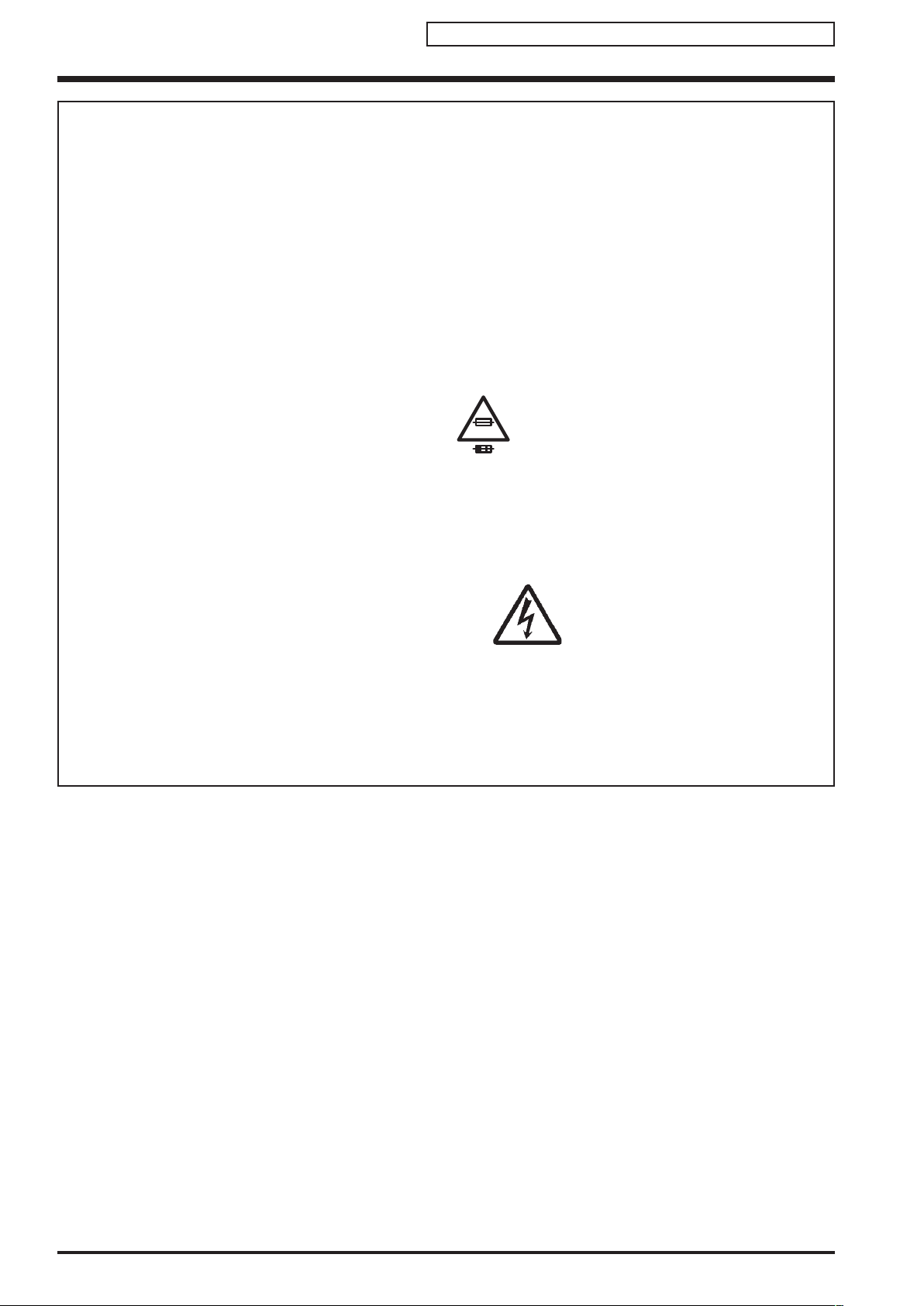
WARNING
THE COMPONENTS IDENTIFIED WITH THE MARK "
" ON THE SCHEMATIC DIAGRAM
AND IN THE PARTS LIST ARE CRITICAL FOR SAFETY.
PLEASE REPLACE ONLY WITH THE COMPONENTS SPECIFIED ON THE SCHEMATIC
DIAGRAM AND IN THE PARTS LIST.
IF YOU USE PARTS NOT SPECIFIED, IT MAY RESULT IN A FIRE AND AN ELECTRICAL
SHOCK.
CAUTION
BECAUSE THIS PRODUCTIS RoHS LEAD-FREE COMPLIANT, USE THE DESIGNATED
AFTER-SELES PARTS AND THE DESIGNATED LEAD-FREE SOLDER WHEN
PERFORMING REPAIRS.
(Refer to page 3 to page 5)
Confidential: FUJIFILM Service Center Use Only
Page 2
FinePix S5800/S800 Service Manual
2
Confidential: FUJIFILM Service Center Use Only
1. Check the area of your repair for unsoldered or poorly
soldered connections. Check the entire board surface
for solder splasher and bridges.
2. Check the interboard wiring to ensure that no wires
are "pinched" or contact high-wattage resistors.
3. Look for unauthorized replacement parts, particularly
transistors, that were installed during a previous
repair. Point them out to the customer and recommend
their replacement.
4. Look for parts which, though functioning, show
obvious
signs of deterioration. Point them out to the customer
and recommend their replacement.
5. Check the B + voltage to see it is at the values
specified.
6. Make leakage - current measurements to determine
that exposed parts are acceptably insulated from
the supply circuit before returning the product to the
customer.
7. CAUTION: FOR CONTINUED
PROTECTION AGAINST FIRE
HAZARD, REPLACE ONLY WITH
SAME TYPE 2.5 AMPERES 125V
FUSE.
ATTENTION: AFIN D'ASSURER
UNE PROTECTION
PERMANENTE CONTRE
LES RISQUES D'INCENDIE,
REMPLACER UNIQUEMENT
PAR UN FUSIBLE DE MEME,
TYPE 2.5 AMPERES, 125
VOLTS.
8. WARNING:
TO REDUCE THE ELECTRIC
SHOCK, BE CAREFUL TO
TOUCH THE PARTS.
SAFETY CHECK-OUT
After correcting the original problem, perform the following
safety check before return the product to the customer.
WARNING!
HIGH VOLTAGE
2.5A 125V
2.5A 125V
RISK OF FIREREPLACE FUSE
AS MARKED
Page 3

FinePix S5800/S800 Service Manual
3
Confidential: FUJIFILM Service Center Use Only
RoHS lead-free compliance
Because this product is RoHS lead-free compliant, use the designated after-sales parts and the designated lead-free solder
when performing repairs.
<Background & Overview>
With the exception of parts and materials expressly excluded from the RoHS directive
(*1)
, all the internal connections and
component parts and materials used in this product are lead-free compliant
(*2)
under the European RoHS directive.
*1: Excluded items (list of the main lead-related items)
• Lead included in glass used in fluorescent tubes, electronic components and cathode-ray tubes
• Lead in high-melting-point solder (i.e. tin-lead solder alloys that contain 85% lead or more)
• Lead in ceramic electronic parts (piezo-electronic devices)
• Mercury contained in fluorescent tubes is also excluded.
*2: Definition of lead-free
A lead content ratio of 0.1 wt% or less in the applicable locations (solder, terminals, electronic components, etc.)
<Reference>
RoHS: The name of a directive issued by the European Parliament aimed at restricting the use of
certain designated hazardous substances included in electrical and electronic equipment.
Designated substances (6): Lead, mercury, cadmium, hexavalent chromium, polybrominated biphenyls (PBBs) and
polybrominated diphenyl ether (PBDE)
<Lead-free soldering>
When carrying out repairs, use a designated lead-free solder, bearing in mind the differing work practices for conventional
solder (eutectic) and lead-free solder.
Differences in the soldering work for lead-free and eutectic solder
When the soldering work practices for eutectic solder and lead-free solder are compared, the main differences are as
shown below. In particular, when lead-free solder is used, the solder tends to be less workable than when eutectic solder is
used. Accordingly, the soldering techniques used must take that into account.
Difference Countermeasure
1 The solder starts melting later. The initial melting point of lead-free solder is high, so you
have to get used to it.
2 Poor wetting Move the tip of the soldering iron around to heat the entire
connection to the melting temperature and assist wetting.
3 Solder feed rate is difficult to control. Use the solder (wire) diameter and soldering iron that are
best suited to connection being soldered.
4 Wetting the insides of through holes is especially
difficult.
First apply solder to the area immediately around the
through hold and then feed the solder into the hole.
5 During repairs (or modifications) removing solder
from inside through holes is difficult.
Use a suitable wicking wire (with a suitable method and
heating) and a suction tool.
6 There is serious carbonization of the soldering iron. Either put solder onto the soldering iron tip after completing
the work, or turn the iron off frequently.
7 The surface is not glossy. Learn to recognize the appearance of the surface.
Page 4

FinePix S5800/S800 Service Manual
4
Confidential: FUJIFILM Service Center Use Only
Setting temperature during lead-free soldering
• Lead-free solder melting temperature
The melting point of eutectic (Sn-Pb) solder is 183°C, while the melting point of lead-free solder (Sn-Ag-Cu) is 30°C
higher at 220°C.
• Soldering iron tip temperature
The temperature setting for the soldering iron used should be such that the tip of the soldering iron is at the correct
bonding temperature for the connection. This temperature is normally set at around 100°C higher than the melting point
of the solder.
However, the actual temperature should take into account the shape and size of the soldering iron tip, the heat tolerance
of the connection and the workability of that temperature.
• Correct bonding temperature
The correct bonding temperature refers not to the temperature of the heat source, but to the bonding temperature that
will give the best bond strength.
Precautions when soldering with lead-free solder
• Soldering iron maintenance
Because of the high soldering iron temperature in lead-free soldering, there is rapid carbonization of the flux adhering to
the tip of the soldering iron.
(1) Always cover the tip of the soldering iron with solder when it is not being used.
(2) If the tip is black from carbonization, wipe it gently with a paper towel soaked in alcohol until the solder will wet.
• Uniform heating of the board and components
To ensure that the lead-free solder wets the entire surface of the pattern and the lands despite its poor wetting
characteristics, you must move the tip of the soldering iron over a wide area to raise the temperature of the entire
connection.
Soldering iron
A soldering iron with a temperature control is best.
Page 5
FinePix S5800/S800 Service Manual
5
Confidential: FUJIFILM Service Center Use Only
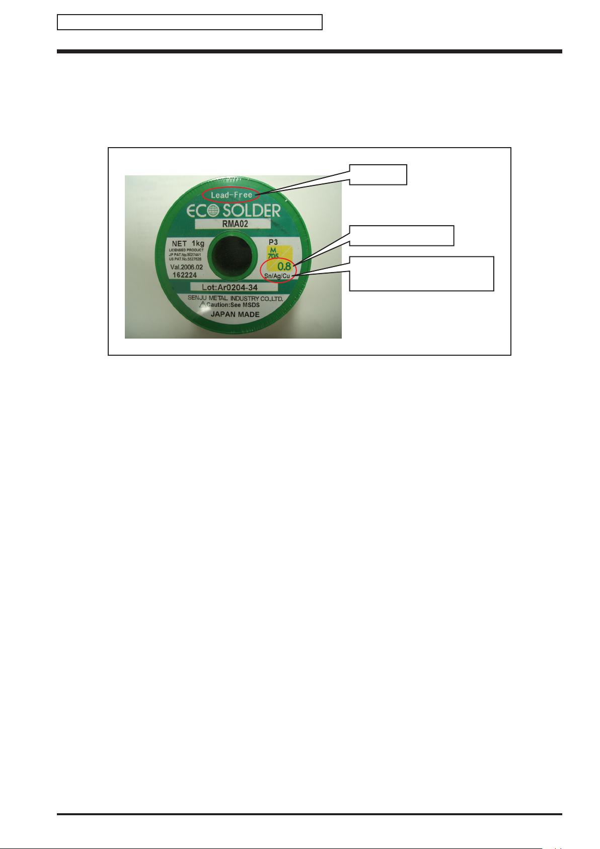
Solder wire (thread)
Use the lead-free solders specified below.
Solder type: Sn96.5Ag3Cu0.5 (Displayed symbol: SnAgCu)
Wire diameter: 0.6, 0.8 or 1.0 mm
Sample:
Flux
Conventional flux can be used.
Solder application wires (mesh, wicking wire, etc.)
Conventional application wires can be used.
lead-free
Wire diameter 0.8mm
Solder type (Displayed symbol)
SnAgCu
Page 6

FinePix S5800/S800 Service Manual
6
Confidential: FUJIFILM Service Center Use Only
MEMO
Page 7

FinePix S5800/S800 Service Manual
7
CONTENTS
Confidential: FUJIFILM Service Center Use Only
CONTENTS
1. General ....................................................... 1-1
1-1. Product specification ............................................1-1
1-2. Explanation of Terms ...........................................
1-4
1-3. Names of External Components ..........................
1-5
2. Disassembly ............................................... 2-1
2-1. Names of internal Components ...........................2-1
2-2. Removing the REAR CONST ..............................
2-2
2-3. Disassembling the REAR CONST .......................
2-3
2-4. Removing the LCD ..............................................
2-4
2-5. Removing the COMPL PWB,CP-1 ......................
2-5
2-6. Removing the SIDE CABI ....................................
2-7
2-7. Removing the LENS ............................................
2-8
2-8. Removing the FLASH UNIT and EVF UNIT ......
2-10
2-8-1. Disassembling the FLASH UNIT ..........
2-11
2-8-2. Disassembling the ST HOLDER ..........
2-13
2-9. Disassembling the LENS
HOLDER TOP ...........2-15
2-10. Disassembling the CABI FRONT .......................
2-17
2-11. Affixing locations for SPACERS and
SHEETS ............................................................2-18
2-11-1. Attaching the SPACER to the
COMPL PWB,CP-1 ..............................
2-18
2-11-2.
Attaching the
CA-1 HOLDER SHEET A and
CA-1 HOLDER SHEET B to the
CA-1 HOLER ........................................2-18
2-11-3. Attaching the SHEET and SPACER
to the LCD HOLDER ............................ 2-19
2-11-4. Attaching the SPACER,
LCD SPACER A and
LCD SPACER
C to the LCD ................. 2-20
2-11-5. Attaching the LCD SPACER B to the
CABI BACK .......................................... 2-21
2-11-6. Attaching the LENS SPACER and
LCD SPACER B to the
LENS HOLDER TOP ............................
2-21
3. Schematics ................................................. 3-1
3-1. Description of CCD circuit operation ....................3-1
3-1-1. Overview ................................................
3-1
3-1-2. IC931 (CCD imager) ..............................
3-1
3-1-3. IC901 (V driver) and IC905 (H driver) ....
3-2
3-1-4. IC905 (CDS, AGC and A/D converter) ...
3-2
3-2. Description of CP1 circuit operation ....................
3-2
3-2-1. Circuit Description ..................................
3-2
3-2-2. Outline of Operation ...............................
3-3
3-2-3. LCD Block ..............................................
3-3
3-2-4. EVF Block ..............................................
3-3
3-2-5. Lens Drive Block ....................................
3-3
3-3. Description of PWA Power Circuit Operation .......
3-4
3-3-1. Overview ................................................
3-4
3-4. Description of ST1 flash circuit operation ............
3-5
3-4-1. Charging circuit ......................................
3-5
3-4-2. Flash Circuit ..........................................
3-5
3-5. Description of SYA circuit operation .....................
3-6
3-5-1. Configuration and Functions ..................
3-6
3-5-2. Internal Communications Paths .............
3-7
3-5-3. Key Operations ......................................
3-7
3-5-4. Power Supply Control ............................
3-8
3-6. Block Diagram .....................................................3-9
3-7. Overall connection Diagram ..............................3-10
3-8. Circuit Diagrams ................................................
3-11
3-8-1. CA1 BLOCK .........................................
3-11
3-8-2. CA2 BLOCK .........................................
3-12
3-8-3. CCD BLOCK ........................................
3-13
3-8-4. CP1 BLOCK (DMA) ..............................
3-14
3-8-5. CP1 BLOCK (PWA) .............................
3-15
3-8-6. CP1 BLOCK (STA) ...............................
3-16
3-8-7. CP1 BLOCK (SYA) ...............................
3-17
3-8-8. CP1 BLOCK (TCA) ..............................
3-18
3-8-9. FLASH BLOCK ....................................
3-19
3-8-10. MAIN/LCD DRIVER BLOCK ................
3-20
3-8-11. POWER BLOCK ..................................
3-21
3-8-12. SYSTEM CONTROL BLOCK ...............
3-22
3-8-13. LENS BLOCK .......................................
3-23
3-8-14. PW1 BLOCK ........................................
3-24
3-8-15. TB1 BLOCK .........................................
3-25
3-8-16. TB2 BLOCK .........................................
3-26
3-9. Mounted Parts Diagrams ...................................
3-27
3-9-1. CA1 PWB
ASSY ...................................3-27
3-9-2. CA2 PWB ASSY ...................................
3-28
3-9-3. TB1 PWB ASSY ...................................3-29
3-9-4. TB2 PWB ASSY ...................................3-29
3-9-5. MAIN PWB ASSY .................................
3-31
Page 8

FinePix S5800/S800 Service Manual
8
CONTENTS
Confidential: FUJIFILM Service Center Use Only
4. Adjustments ............................................... 4-1
4-1. Important point before adjustment .......................4-1
4-1-1. The handling of image files in
internal memory .....................................4-1
4-1-2. Adjustment when Replacing
Major Parts .............................................4-2
4-2. Measuring instruments used ................................
4-2
4-3. Use jig ..................................................................
4-2
4-4. Calibration method of pattern box ........................
4-3
4-5. Adjustment software installation ..........................
4-3
4-5-1. Various downloading software
decompressions,
preservation methods, and notes ...........4-3
4-6. Connecting to the PC for Adjustment ...................
4-4
4-7. Adjustment Software Description .........................
4-5
4-8. MAIN PWB ASSY initialization .............................
4-6
4-9. LENS Adjustment ...............................................
4-10
4-10. AWB Adjustment ................................................
4-13
4-11. CCD Defect Detection .......................................
4-15
4-12. CCD Black Defect Detection ..............................
4-17
4-13. Updating the Firmware ......................................
4-19
4-14. Completion Settings ...........................................
4-22
5. Inspection ................................................... 5-1
5-1. Required Measuring Equipment ..........................5-1
5-2. Connection of Measuring Equipment ...................
5-1
5-3. Inspection and Factory Settings ..........................
5-2
CONTENTS
6. Parts List .................................................... 6-1
6-1. Packing and Accessories .....................................6-1
6-1-1. US-model
(S800) ...................................6-1
6-1-2. EU-model
(S5800) .................................6-2
6-1-3. EG-model
(S5800) .................................6-3
6-1-4. EE-model
(S5800) ..................................6-4
6-1-5. CH-model (S5800) .................................
6-5
6-2. Mechanical Block 1 ..............................................
6-7
6-2-1. US/EU/EG/EE/CH-model
(S5800/S800) ......................................... 6-7
6-3. Mechanical Block 2 ..............................................
6-8
6-3-1. US-model (S800) ...................................
6-8
6-3-2. EU/EG/EE-model (
S5800) .....................6-9
6-3-3. CH-model
(S5800) ...............................6-10
6-4. Flash Block ........................................................
6-11
6-4-1. US-model (S800) .................................
6-11
6-4-2. EU/EG/EE/CH-model (
S5800) .............6-12
6-5. Electrical parts ...................................................
6-13
7. Appendix .................................................... 7-1
7-1. List of Related Technical Updates Issued ............7-1
Page 9

FinePix S5800/S800 Service Manual
1-1
1. General
Confidential: FUJIFILM Service Center Use Only
1. General
1-1. Product specification
System
Model Digital camera FinePix S5800 / S800
Effective pixels 8.0 million pixels
CCD 1/2.5-inch CCD
Storage media Internal memory (approx. 26 MB)
xD-Picture Card (16/32/64/128/256/512 MB/1 GB/2 GB)/SD Memory Card (FUJIFILM
recommendation)
File format Still image: DCF-compliant
Compressed: Exif ver.2.2 JPEG, DPOF-compatible
* Design rule for Camera File System compliant/DPOF compatible
Movie: AVI format, Motion JPEG
Audio: WAVE format, Monaural sound
Number of recorded 3264 × 2448 pixels/3264 × 2176 pixels/2304 × 1728 pixels/1600 × 1200 pixels/
pixels (Still image) 640 × 480 pixels (
/ / / / )
Lens Fujinon 10× optical zoom lens F3.5-F3.7
Focal length f=6.33 mm-63.3 mm (Equivalent to approx. 38 mm-380 mm on a 35 mm camera)
Digital zoom Approx. 5.1× (10× optical zoom lens is used together: Max. zoom scale: approx. 51×)
Aperture (Wide-angle) F3.5 to F13.6, 7 steps in 1/3 EV increments Manual/Auto selectable
Focal range Normal: Wide-angle: approx. 30 cm (1.0 ft.) to infinity (In High-speed shooting mode:
approx. 1.0 m (3.3 ft.) to infinity)
Telephoto: approx. 1.0 m (3.3 ft.) to infinity (In High-speed shooting mode: approx.
1.0 m (3.3 ft.) to infinity)
Macro: Wide-angle: 4 cm to 3.0 m (1.6 in. to 9.8 ft.)
Telephoto: 60 cm to 3.0 m (2.0 ft. to 9.8 ft.)
Super macro: approx. 1 cm to 1.0 m (0.4 in. to 3.3 ft.) (Wide-angle only)
Sensitivity Auto/Auto (800)/Auto (400)/Equivalent to 64/100/200/400/800/1600 (Standard output
sensitivity)
Photometry TTL 256-zones metering Multi, Spot, Average
Exposure control Program AE (When using P mode : Program Shift is enabled)/Shutter priority AE/Aperture
priority AE/Manual exposure
Scene position
(NATURAL LIGHT), (NATURAL & ), (PORTRAIT), (LANDSCAPE),
(SPORT), (NIGHT), (FIREWORKS), (SUNSET), (SNOW), (BEACH),
(MUSEUM), (PARTY), (FLOWER), (TEXT)
Picture Stabilization Available
Exposure compensation -2 EV to +2 EV in 1/3 EV-step increments (P, A, S)
Shutter speed
, , , , , , , , , , , , : 1/4 sec. to 1/1000 sec*.
: 3 sec. to 1/1000 sec.*
: 4 sec. to 1/2 sec.*
: 1/4 sec. to 1/1000 sec.* (flash only).
P, A, S: 4 sec. to 1/1000 sec.*
M: 4 sec. to 1/1000 sec.* *depend on Exposure mode
Continuous shooting Top-3: Number of recorded frames: up to 3 frames (Max. 1.3 frames/sec.)
Long-period: Number of recorded frames:
Depend on memory size. 1.8 sec. interval at
N
depending on quality level. (Max. 0.6 frames/sec.)
Auto bracketing ± 1/3 EV, ± 2/3 EV, ± 1 EV
Focus Mode: Single AF, Continuous AF, Manual focus
AF system: TTL contrast-type, AF-assist illuminator
AF frame selection: AF (CENTER), AF (MULTI), AF (AREA)
Page 10
FinePix S5800/S800 Service Manual
1-2
1. General
Confidential: FUJIFILM Service Center Use Only
System
White balance Automatic scene recognition/Preset (Fine, Shade, Fluorescent (Daylight), Fluorescent (Warm
White), Fluorescent (Cool White), Incandescent) /Custom
Self-timer Approx. 2 sec./10 sec.
Flash type Popping the flash up automatically
Effective range: (
: 800): approx. 50 cm-6.2 m (1.6 ft.-20 ft.)
(Macro): approx. 30 cm-3.0 m (1.0 ft.-9.8 ft.)
Flash mode Auto, Red-eye Reduction, Forced Flash, Suppressed Flash, Slow Synchro, Red-eye
Reduction + Slow Synchro
Viewfinder 0.24 inches, approx. 230,000 pixels low-temperature polysilicon TFT color LCD finder,
Approx. 97% coverage
LCD monitor 2.5 inches, Aspect ratio: 4:3; approx. 230,000 pixels low-temperature polysilicon TFT color
LCD monitor, Approx. 97% coverage
Movie 640 × 480 pixels/320 × 240 pixels (
/ )
(30 frames per second with monaural sound)
A series of continuous image can be recorded depending on the available space on an
Memory Card or internal memory.
A movie recording will stop automatically when a movie file becomes approx. 2GB. If you
want to continue recording another movie, press the shutter button again. The available
recording time is displayed based on approx. 2GB.
Photography functions High-speed shooting, Best framing, Post shot assist window, Frame No. memory,
Histograms
Playback functions Trimming, Slide Show, Multi-frame playback, Sorting by date, Image rotate, Histograms
(Highlight warning), Voice memo
Other functions PictBridge, Exif print, Language (
, English, Francais, Deutsch, , Italiano, ,
, , , , Nederlands, , , Magyar, Polski, Svenska), Time
difference, FinePix photo mode(
-mode), Discharging rechargeable batteries
Quality setting
F N
(30 fps) (30 fps)
Number of recorded
pixels
3264 × 2448 640 × 480 640 × 480 320 × 240
Image data size
3.9 MB 2.0 MB 1.8 MB 980 KB
Internal memory
(approx. 26 MB)
15 27 43 211
xD-Picture Card
16 MB
9 16 25 124
32 MB 18 32 51 249
64 MB
36 64 102 499 1.8 min.
128 MB
72 204 999 3.7 min.
256 MB
145 410 1999 7.4 min.
290 819 3995 14.8 min.
1 GB
581 1640 7996 29.6 min.
2 GB 1163 2063 3199 15995
59.2 min.
SD
Memory
Card
281 793 3868 14.3 min.
1 GB 563 1589 7746 28.7 min.
2 GB 1127 3100 15504 57.4 min.
SDHC
Memory
Card
4 GB 2229 6131 30655
8 GB
6
4
8
16
32
65
130
261
520
126
252
504
996
1995
13
8
16
32
64
130
259
520
1031
251
503
1000
1977
3959 4463 12275 61375
Standard number of available frames/recording time per xD-Picture Card, SD Memory Card and internal memory
The nu m ber of ava i lab le f ram es a nd r eco rdin g t i me is a ppr oxim ate . Ac tual nu m ber of fra mes and
rec ord i ng time va r ies de p end ing on t he type s o f Me mor y Ca rd o r s h oot ing con d iti on. Als o, t he n umb er o f
fra mes and rec ord i ng tim e di spla yed in the LCD mon ito r ma y no t d e cre ase reg u lar ly
.
512 MB
512 MB
*A mov ie re cordi ng wi ll st op au tomat icall y whe n a m ovie file becom es ap prox. 2GB. If y ou wa nt to cont inue
recor ding anoth er mo vie, press the shutt er bu tton again . The avai lable reco rding time is d ispla yed b ased on ap prox. 2GB.
3264 × 2176 2304 × 1728 1600 × 1200
630 KB 130 KB –– ––
29 sec. 46 sec.
17 sec. 27 sec.
55 sec.34 sec.
70 sec.
2.3 min.
113.5 min.*
227.3 min.*
4.7 min.
9.3 min.
18.7 min.
36.8 min.
9 min.
18.1 min.
35.6 min.
70.5 min.*
141.1 min.*
128
257
515
1031
499
999
2000
3955
7919
Page 11

FinePix S5800/S800 Service Manual
1-3
1. General
Confidential: FUJIFILM Service Center Use Only
Alkaline batteries
Ni-MH batteries 2500 mAh
Battery Type With LCD monitor ON With viewfinder (EVF) ON
Approx. 300 frames
Approx. 500 frames
Approx. 300 frames
Approx. 500 frames
Input/Output Terminal
A/V OUT NTSC/PAL-type (with monaural sound)
(Audio/Visual output)
Digital input/output USB 2.0 Full-Speed, PTP (Picture Transfer Protocol)/MTP (Media Transfer Protocol)
DC input socket AC Power Adapter AC-5VX (sold separately)
Power Supply and Others
Power supply Use one of the following:
• 4× AA-size alkaline batteries
• 4× AA-size Ni-MH (Nickel-Metal Hydride) batteries (sold separately)
• AC Power Adapter AC-5VX (sold separately)
Guide to the number of
available frames for
battery operation
According to the CIPA (Camera & Imaging Products Association) standard procedure for
measuring digital still camera battery consumption (extract):
When using alkaline batteries, use the batteries supplied with the camera. You can use Ni-
MH batteries also. The storage media should be xD-Picture Card.
Pictures should be taken at a temperature of +23
o
C (+73oF), with the LCD monitor turned
on, the optical zoom moved from full wide-angle to full telephoto (or vice-versa) and back
again to its original position every 30 seconds, the flash used at full power every second
shot and the camera turned off and then on again once every 10 shots.
• Note: Because the number of available shots varies depending on the capacity of alkaline
batteries or the level of charge in Ni-MH batteries, the figures shown here for the
number of available shots using batteries are not guaranteed.
The number of available shots will also decline at low temperatures.
Camera dimensions 106.1 mm × 75.7 mm × 80.7 mm/4.2 in. × 3.0 in. × 3.2 in.
(W/H/D) (not including accessories and attachments)
Camera mass (weight) Approx. 307 g/10.8 oz. (not including accessories, batteries and Memory Card)
Weight for photography Approx. 402 g/14.2 oz. (including batteries and Memory Card)
Operating conditions Temperature: 0
o
C to +40oC (+32oF to +104oF)
80% humidity or less (no condensation)
Accessories included
AA-size Alkaline Batteries (LR6) (4)
Strap (1)
Lens cap (1 set)
A/V cable (1)
USB cable (1)
CD-ROM (1) Software for FinePix CX
Owner’s Manual (1)
Optional accessories
xD-Picture Card
256MB/512MB/1GB/2GB
AC Power Adapter AC-5VX
PC Card Adapter DPC-AD
• Compatible with xD-Picture Card of 16 MB to 512 MB, and SmartMedia of 3.3 V,
2 MB to 128 MB.
CompactFlash Card Adapter DPC-CF
Page 12

FinePix S5800/S800 Service Manual
1-4
1. General
Confidential: FUJIFILM Service Center Use Only
1-2. Explanation of Terms
Deactivated batteries: Leaving an Ni-MH battery unused in storage for a long period may cause a rise in the level
of substances that inhibit current flow inside the battery and result in a dormant battery. A
battery in this state is referred to as deactivated.
Because current flow is inhibited in a deactivated Ni-MH battery, the battery’s original level
of performance cannot be achieved.
EV: A number denotes Exposure Value. The EV is determined by the brightness of the subject
and sensitivity (speed) of the film or CCD. The number is larger for bright subjects and
smaller for dark subjects. As the brightness of the subject changes, a digital camera main
-
tains the amount of light hitting the CCD at a constant level by adjusting the aperture and
shutter speed.
When the amount of light striking the CCD doubles, the EV increases by 1. Likewise, when
the light is halved, the EV decreases by 1.
Frame rate (fps): The frame rate refers to the number of images (frames) that are photographed or played
back per second. For example, when 10 frames are continuously photographed in a 1-sec
-
ond interval, the frame rate is expressed as 10 fps.
For reference, TV images are displayed at 30 fps (NTSC).
JPEG: Joint Photographic Experts Group
A file format used for compressing and saving color images. The higher the compression
rate, the greater the loss of quality in the decompressed (restored) image.
Memory effect: If an Ni-MH battery is repeatedly charged without first being fully discharged, its perfor
-
mance may drop below its original level.
This is referred to as the “memory effect”.
Motion JPEG: A type of AVI (Audio Video Interleave) file format that handles images and sound as a single
file. Images in the file are recorded in JPEG format. Motion JPEG can be played back by
QuickTime 3.0 or later.
Smear: A phenomenon specific to CCDs whereby white streaks appear on the image when there is
a very strong light source, such as the sun or reflected sunlight, in the photography screen.
WAVE A standard format used on Windows systems for saving audio data. WAVE files have the
“.WAV” file extension and the data can be saved in either compressed or uncompressed
format. Uncompressed recording is used on this camera.
WAVE files can be played back on a personal computer using the following software:
Windows: MediaPlayer
Macintosh: QuickTime Player
* QuickTime 3.0 or later
White Balance: Whatever the kind of the light, the human eye adapts to it so that a white object still looks
white. On the other hand, devices such as digital cameras see a white subject as white by
first adjusting the color balance to suit the color of the ambient light around the subject. This
adjustment is called matching the white balance.
Exif Print: Exif Print Format is a newly revised digital camera file format that contains a variety of
shooting information for optimal printing.
Page 13

FinePix S5800/S800 Service Manual
1-5
1. General
Confidential: FUJIFILM Service Center Use Only
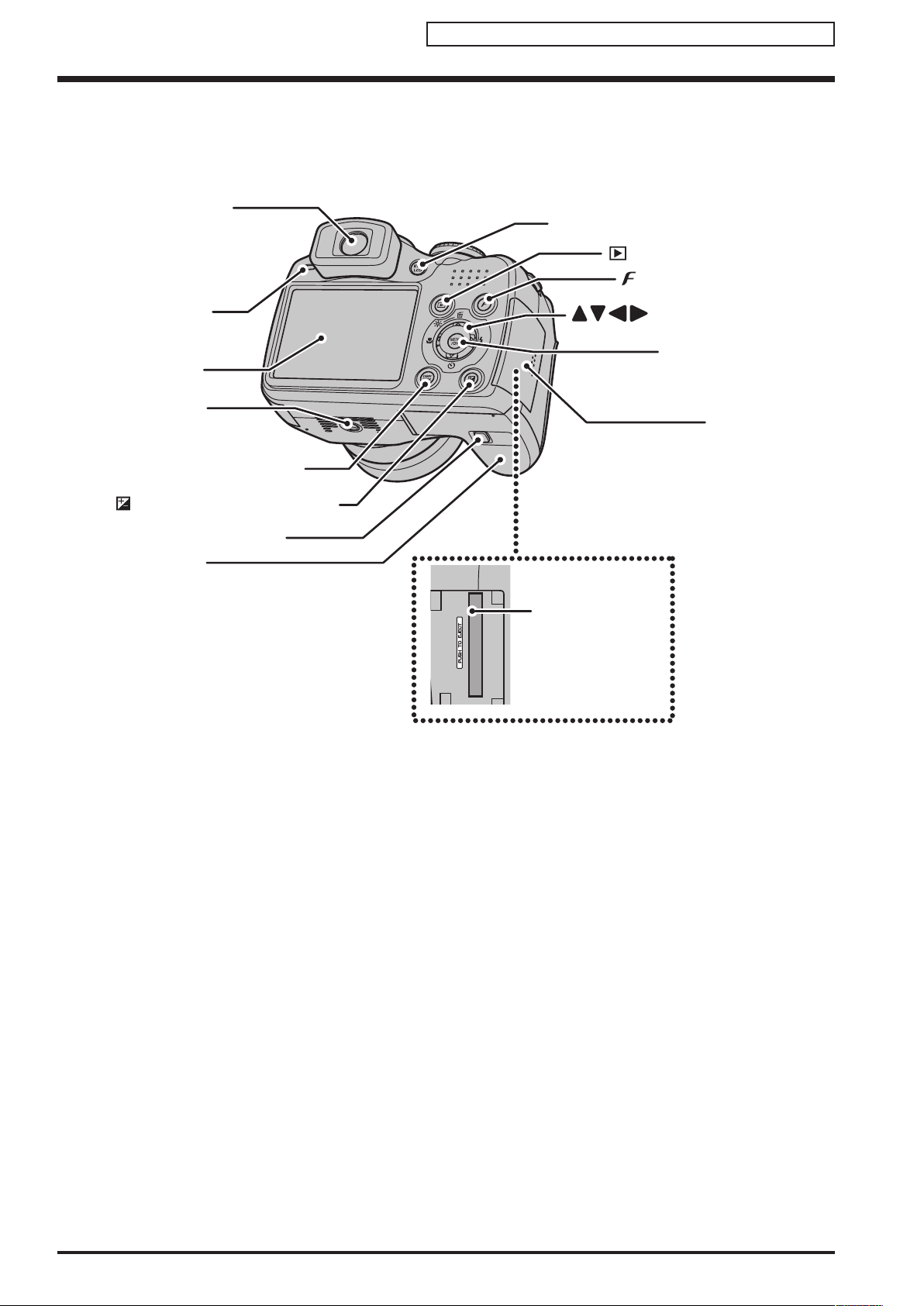
1-3. Names of External Components
Strap mount
Strap moun
t
Zoom leve
r
Power switch
Mode dial
Continuous
shooting button
Shutter button
Microphon
e
Speake
r
Terminal cove
r
A
F-assist illuminator/
Self-timer lamp
USB socket/A/V OUT
(Audio/Visual output) socket
DC IN 5V (power input) socket
Auto popup flash
Page 14
FinePix S5800/S800 Service Manual
1-6
1. General
Confidential: FUJIFILM Service Center Use Only
Viewfinder (EVF)
Indicator lamp
LCD monitor
Tripod mount
DISP (Display)/BACK button
Exposure compensation button
Cover lock release button
Battery cover
EVF/LCD (monitor selector) button
Playback mode button
(Photo mode) button
(4-direction) button
MENU/OK button
Slot cove
r
Memory Card slot
Page 15
FinePix S5800/S800 Service Manual
2-1
2. Disassembly
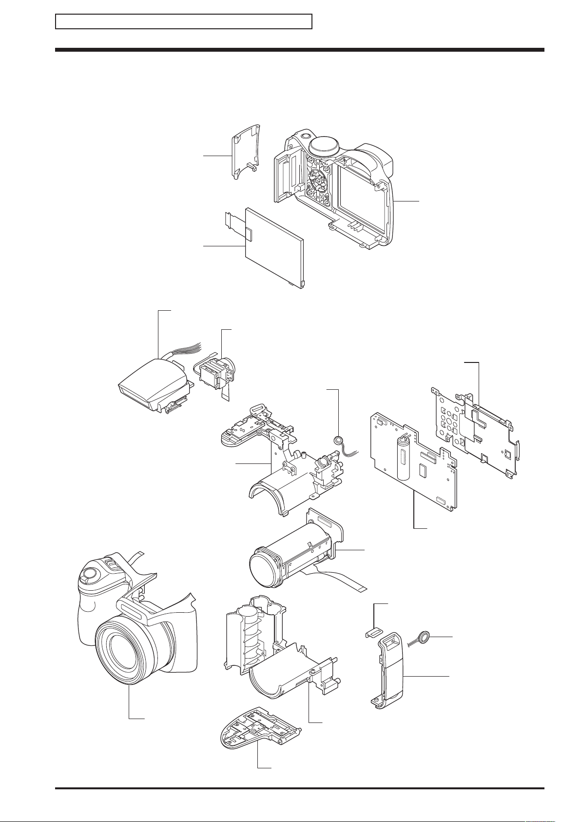
Confidential: FUJIFILM Service Center Use Only
2. Disassembly
2-1. Names of internal Components
LENS ASSY
STRAP LENS HOLDER
LENS HOLDER BOTTOM
SIDE CABI
SPEAKER
CABI FRON
T
LCD HOLDER
LENS HOLDER TOP
BATTERY COVER
MICROPHONE
FLASH ASSY
EVF UNIT
COMPL PWB CP-1
CABI BACK
LCD MONITOR
CARD COVER
Page 16

FinePix S5800/S800 Service Manual
2-2
2. Disassembly
Confidential: FUJIFILM Service Center Use Only
3
4
1
2
5
6
7
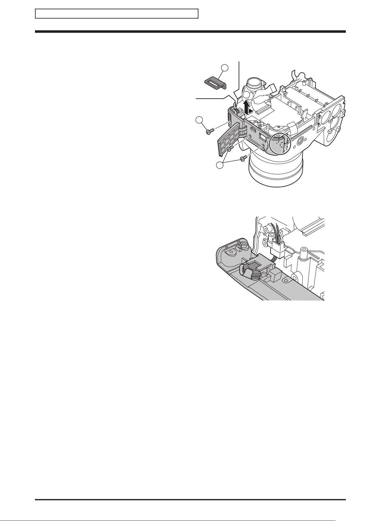
2-2. Removing the REAR CONST
(1) Remove the 1 screw (1.7 x 6.0).
(2) Remove the 2 screws (1.7 x 6.0).
(3) Remove the screw (1.7 x 4.0).
(4) Open the BATTERY COVER and remove the screw
(1.4 x 3.0).
(5) Lift off the REAR CONST in the direction of the arrow.
[Notes]
• Raise the REAR CONST slowly because the MODE
FPC is connected to the COMPL PWB, CP-1.
• Take care not to drop the CARD COVER.
(6) Unlock the connector and disconnect the flexible
cable.
[Assembly]
Install the CARD COVER on the REAR CONST and the
BATTERY COVER on the CABI FRONT and assemble by
carrying out the disassembly procedure in reverse.
(7) Remove the BATTERY COVER.
[Notes on Assembly]
Take care with the routing of the LENS FPC.
Page 17

FinePix S5800/S800 Service Manual
2-3
2. Disassembly
Confidential: FUJIFILM Service Center Use Only
3
2
1
4
3
7
5
8
MODE CLICK SPRING
6
MODE DIAL KNOB
6
MODE DIAL SPRING
6
2-3. Disassembling the REAR CONST
(1) Remove the 2 screws (1.7 x 3.0).
(2) Remove the BUTTON BASE in the direction of the
arrow.
(3) Remove the 3 screws (1.4 x 3.0).
(4) Remove the MODE HOLDER PLATE in the direction
of the arrow, taking care with the catches on the
MODE DIAL HOLDER.
(5) Hold the MODE DIAL KNOB to one side with your
hand and remove the screw (1.7 x 3.0).
(6) Remove the MODE DIAL SPRING, MODE CLICK
SPRING and MODE DIAL KNOB.
(7) Remove the screw (1.4 x 3.0).
(8) Remove the MODE DIAL HOLDER.
[Notes]
Take care not to bend the MODE DIAL SPRING section.
[Assembly]
Assemble by performing the disassembly procedure in
reverse.
Page 18

FinePix S5800/S800 Service Manual
2-4
2. Disassembly
Confidential: FUJIFILM Service Center Use Only
3
1
2
2-4. Removing the LCD
(1) Peel off the SHEET SHADE.
(2) Raise the LCD in the direction of the arrow.
(3) Unlock the connector and remove the LCD.
[Assembly]
Assemble by performing the disassembly procedure in
reverse.
Page 19

FinePix S5800/S800 Service Manual
2-5
2. Disassembly
Confidential: FUJIFILM Service Center Use Only
1
2
3
11
13
4
7
6
5
12
9
10
8
2-5. Removing the COMPL PWB,CP-1
(1) Remove the 5 screws (1.7 x 4.0).
(2) Remove the LCD HOLDER in the direction of the
arrow.
(3) Remove the screw (1.7 x 4.0).
(4) Discharge the main capacitor.
Take care not to touch the main capacitor terminals
before discharging the capacitor.
(5) Remove the solder in 2 locations on the SPEAKER
lead wires.
(6) Remove the solder in 2 locations on the
MICROPHONE lead wires.
(7) Remove the solder in 4 locations on the lead wires
from the EVF UNIT.
(8) Remove the adhesive and then remove the solder in
4 locations on the lead wires from the FLASH ASSY.
(9) Remove the solder in 2 locations on the AF LED
lead wires.
(10) Remove the adhesive and then remove the solder in
2 locations on the lead wires from the COMPL PWB,
PW-1.
(11) Unlock the connector and remove the LENS FPC.
(12) Release the 2 connector locks and remove the FPC
for the EVF UNIT.
(13) Lift up the COMPL PWB, CP-1 in the direction of the
arrow.
Page 20

FinePix S5800/S800 Service Manual
2-6
2. Disassembly
Confidential: FUJIFILM Service Center Use Only
Red
Red
Red
Gray
Gray
Pink
Gray
White
White
White
Black
Black
Black
Pink
White
Gray
(14) Unlock the connector and remove the FPC.
(15) Unlock the connector and remove the FPC for the
ZOOM SW UNIT.
[Assembly]
Assemble by performing the disassembly procedure in
reverse.
[Notes on Assembly]
• Take care to route the EVF UNIT FPC correctly.
15
14
Page 21
FinePix S5800/S800 Service Manual
2-7
2. Disassembly
Confidential: FUJIFILM Service Center Use Only
2-6. Removing the SIDE CABI
(1) Open the JACK COVER and remove the 2 screws (1.7
x 3.0).
(2) Remove the screw (1.7 x 6.0).
(3) Remove the SIDE CABI in the direction of the arrow,
taking care with the SPEAKER lead wires.
(4) Remove the STRAP LENS HOLDER.
[Assembly]
Assemble by performing the disassembly procedure in
reverse.
[Notes on Assembly]
Stowing the SPEAKER lead wires as shown in figure.
2
3
1
4
Page 22

FinePix S5800/S800 Service Manual
2-8
2. Disassembly
Confidential: FUJIFILM Service Center Use Only
2-7. Removing the LENS
(1) PEEL off the CA-1 HOLDER SHEET A.
(2) Remove the screw (1.4 x 2.5).
(3) Remove the EARTH HOLDER A.
(4) Remove the 2 screws (1.4 x 3.0).
(5) Remove the EARTH HOLDER B.
(6) Remove the CA-1 HOLDER.
(7) Remove the STRAP EARTH.
(8) Remove the 4 screws (1.7 x 4.0).
(9) Press straight down on the SLIDE RETURN
HOLDER (pale orange) and pop up the FLASH
UNIT.
(10) Lift up the LENS HOLDER BLOCK in the direction of
the arrow.
1
2
3
5
6
4
7
10
9
8
Page 23

FinePix S5800/S800 Service Manual
2-9
2. Disassembly
Confidential: FUJIFILM Service Center Use Only
14
15
(11) Peel off the SHEET LENS FPC.
[Notes]
When peeling off the SHEET LENS FPC, take care not to
break any wires in the LENS FPC.
(12) Peel off the SHEET LEAD POWER.
(13) Remove the 5 screws (1.7 x 4.0).
(14) Release the 2 catches and remove the LENS
HOLDER TOP in the direction of the arrow.
[Notes]
• When removing the LENS from the LENS HOLDER
BOTTOM, take care not to break any wires in the LENS
FPC.
(15) Remove the LENS.
[Assembly]
Assemble by performing the disassembly procedure in
reverse.
12
11
13
13
[Notes on Assembly]
Stowing the lead wires as shown in figure.
Page 24

FinePix S5800/S800 Service Manual
2-10
2. Disassembly
Confidential: FUJIFILM Service Center Use Only
1
2
3
5
4
2-8. Removing the FLASH UNIT and EVF UNIT
(1) Remove the 2 screws (1.7 x 4.0).
(2) Remove the FLASH UNIT in the direction of the
arrow.
(3) Peel off the SHEET EVF B.
(4) Remove the screw (1.7 x 3.0).
(5) Remove the EVF UNIT.
[Assembly]
Assemble by performing the disassembly procedure in
reverse.
Page 25

FinePix S5800/S800 Service Manual
2-11
2. Disassembly
Confidential: FUJIFILM Service Center Use Only
1
2
347
9
6
5
10
11
12
8
2-8-1. Disassembling the FLASH UNIT
(1) Slide the SLIDE RETURN HOLDER in the direction
of the arrow and pop up the FLASH UNIT.
(2) Remove the 2 screws (1.7 x 4.0).
(3) Remove the ST COVER TOP in the direction of the
arrow.
(4) Push out the ST SHAFT in the direction of the arrow.
(5) Remove the ST POP SPRING.
(6) Push out the ST COVER SHAFT in the direction of
the arrow.
(7) Remove the ST COVER BOTTOM.
(8) Peel off the SHEET ST A.
(9) Remove the 4 lead wires from the ST COVER
BOTTOM guide slot and pull out the TUBE.
(10) Remove the solder in 1 location and remove the
TRANS.
(11) Remove the FLASH HOLDER in the direction of the
arrow.
(12) Remove the FLASH COVER.
Page 26
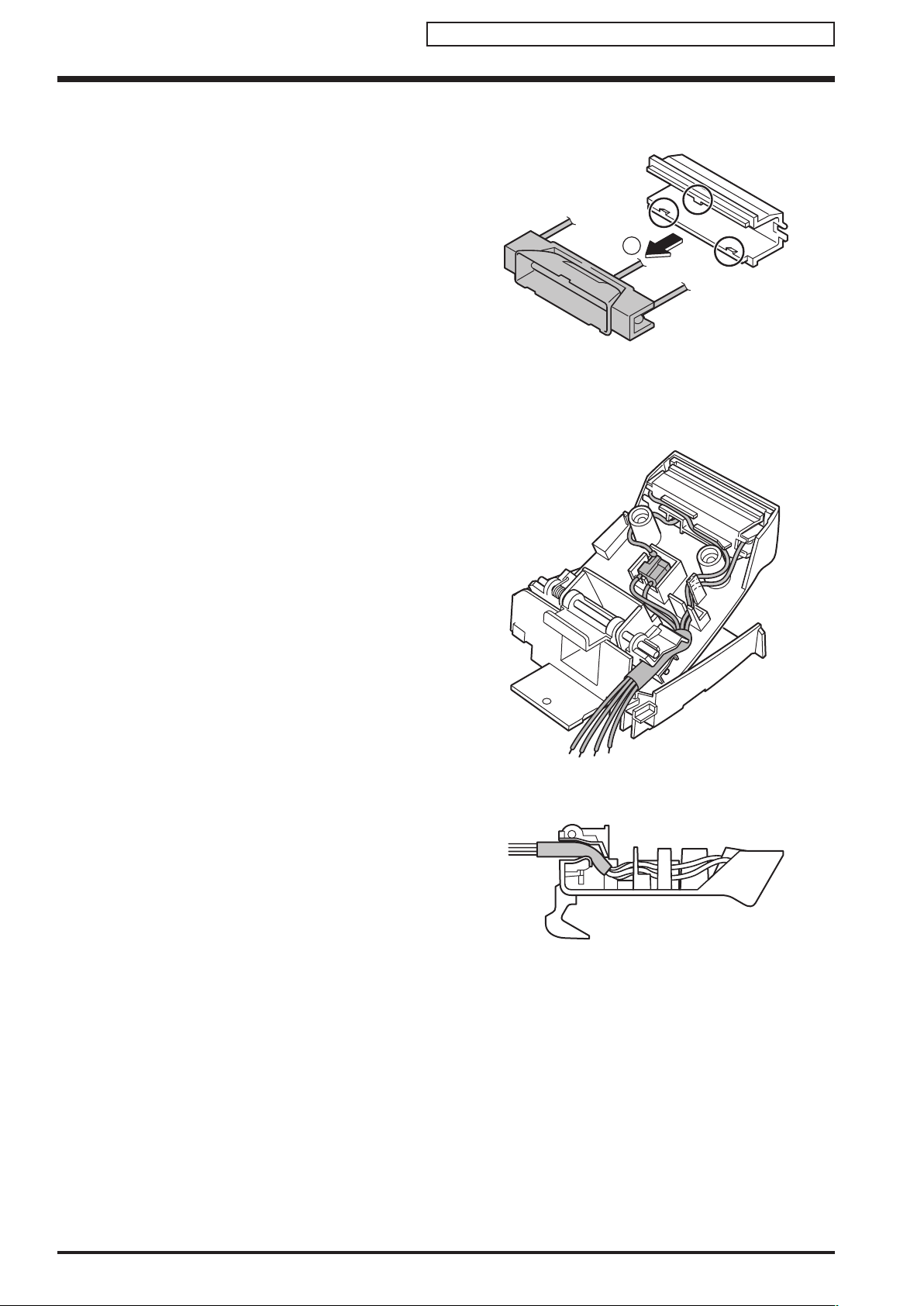
FinePix S5800/S800 Service Manual
2-12
2. Disassembly
Confidential: FUJIFILM Service Center Use Only
13
(13) While releasing the 3 FLASH HOLDER catches,
remove the LAMP ASSY.
[Assembly]
Assemble by performing the disassembly procedure in
reverse.
[Notes on Assembly]
• Stowing the lead wires as shown in figure.
• TUBE positioning.
Page 27

FinePix S5800/S800 Service Manual
2-13
2. Disassembly
Confidential: FUJIFILM Service Center Use Only
1
2
3
5
6
4
B
A
7
11
10
9
8
2-8-2. Disassembling the ST HOLDER
(1) Remove the screw (1.4 x 2.0).
(2) Remove the ST LOCK LEVER.
(3) Remove the LOCK SPRING.
(4) Remove the 2 screws (1.7 x 3.0).
(5) Remove the SLIDE PLATE.
(6) Remove the ST SLIDE HOLDER and SOLENOID
SPRING.
(7) Remove the RETURN SPRING.
(8) Slide the SLIDE RETURN HOLDER in the direction
of arrow (1) and remove it in the direction of arrow (2).
(9) Remove the 2 screws.
(10) Remove the COMPL PWB, TB-2.
(11) Remove the SLD UNIT.
[Assembly]
Assemble by performing the disassembly procedure in
reverse.
Page 28

FinePix S5800/S800 Service Manual
2-14
2. Disassembly
Confidential: FUJIFILM Service Center Use Only
[Notes on Assembly]
• Stowing the lead wires as shown in figure.
• Spring positioning and its meshing location with the
motor.
Page 29

FinePix S5800/S800 Service Manual
2-15
2. Disassembly
Confidential: FUJIFILM Service Center Use Only
2
4
3
5
7
1
6
8
2-9. Disassembling the LENS HOLDER TOP
(1) Remove the MICROPHONE.
(2) Remove the 2 screws (1.7 x 3.0).
(3) Remove the STRAP GRIP HOLDER.
(4) Remove the 2 screws (1.7 x 3.0).
(5) Remove the STRAP GRIP EARTH.
(6) Remove the solder in 4 locations.
(7) While pulling the 2 lead wires out of the groove in
the LENS HOLDER TOP, remove the COMPL PWB,
PW-1.
(8) Remove the 4 screws (1.7 x 2.5) and then remove
BATTERY TERMINAL A and BATTERY TERMINAL
B.
Page 30

FinePix S5800/S800 Service Manual
2-16
2. Disassembly
Confidential: FUJIFILM Service Center Use Only
11
10
12
12
9
Pink
Black
(9) Peel off the AF LED SHEET.
(10) Remove the 2 screws (1.7 x 3.0).
(11) Remove the AF LED HOLDER.
(12) Remove the COMPL PWB,TB-1 and AF LED
SPRING.
[Assembly]
Assemble by performing the disassembly procedure in
reverse.
[Notes on Assembly]
• Stowing the lead wires as shown in figure.
Page 31

FinePix S5800/S800 Service Manual
2-17
2. Disassembly
Confidential: FUJIFILM Service Center Use Only
5
9
7
1
4
2
6
3
3
8
2-10. Disassembling the CABI FRONT
(1) Remove the 2 screws (1.7 x 4.0).
(2) Remove the STAND.
(3) Remove the 8 screws (1.7 x 6.0).
(4) Remove the LENS RING TOP, LENS RING MIDDLE
and LENS RING BOTTOM.
(5) Remove the screw (1.4 x 3.0).
(6) Remove the AF LED COVER.
(7) Remove the screw (1.7 x 2.5).
(8) Remove the 2 screws (1.4 x 3.0).
(9) Remove the ZOOM SW UNIT.
[Assembly]
Assemble by performing the disassembly procedure in
reverse.
Page 32

FinePix S5800/S800 Service Manual
2-18
2. Disassembly
Confidential: FUJIFILM Service Center Use Only
<SIDE A>
<SIDE B>
2-11. Affixing locations for SPACERS and SHEETS
2-11-1. Attaching the SPACER to the COMPL PWB,CP-1
(1) Attach the SPACER to the <SIDE A> as shown in the
figure on the right.
(2) Attach the SPACER to the <SIDE B> as shown in the
figure on the right.
2-11-2. Attaching the CA-1 HOLDER SHEET A and CA-1 HOLDER SHEET B to the CA-1 HOLER
(1) Attach the CA-1 HOLDER SHEET B to the CA-1
HOLDER as shown in the figure on the right.
(2) Attach the CA-1 HOLDER SHEET A to the CA-1
HOLDER as shown in the figure on the right.
2
1
2
Page 33

FinePix S5800/S800 Service Manual
2-19
2. Disassembly
Confidential: FUJIFILM Service Center Use Only
3
2
2-11-3. Attaching the SHEET and SPACER to the LCD HOLDER
(1) Attach the SHEET LCD HOLDER B to the LCD
HOLDER as shown in figure.
(2) Attach the SHEET LCD HOLDER B over the SHEET
LCD HOLDER A as shown in figure.
(3) Attach the MAIN FLAME A and MAIN FLAME B as
shown in figure.
Page 34

FinePix S5800/S800 Service Manual
2-20
2. Disassembly
Confidential: FUJIFILM Service Center Use Only
2-11-4. Attaching the SPACER, LCD SPACER A and LCD SPACER C to the LCD
(1) Attach the SPACER to the LCD as shown in figure.
(2) Attach the two LCD SPACER A to the LCD as shown
in figure.
(3) Attach the LCD SPACER C to cover the SHEET
SHADE as shown in the figure on the right.
3
2
Page 35

FinePix S5800/S800 Service Manual
2-21
2. Disassembly
Confidential: FUJIFILM Service Center Use Only
2-11-5. Attaching the LCD SPACER B to the CABI BACK
Attach the LCD SPACER B to the CABI BACK as shown
in figure.
2-11-6. Attaching the LENS SPACER and LCD SPACER B to the LENS HOLDER TOP
(1) Attach the LENS SPACER to the LENS HOLDER
TOP as shown in figure.
(2) Attach the LCD SPACER B to the LENS HOLDER
TOP as shown in figure.
Page 36

FinePix S5800/S800 Service Manual
2-22
2. Disassembly
Confidential: FUJIFILM Service Center Use Only
MEMO
Page 37

FinePix S5800/S800 Service Manual
3-1
3. Schematics
Confidential: FUJIFILM Service Center Use Only
3. Schematics
3-1. Description of CCD circuit
operation
3-1-1. Overview
The CCD peripheral circuit block is primarily made up of the
following ICs:
IC931 (ICX646COZ) CCD imager
IC905 (AD9971BCPZRL) H driver, CDS, AGC and A/D
converter
IC901 (CXD3445GA) V driver
3-1-2. IC931 (CCD imager)
• Interline CCD image sensor
• Image size: 7.183 mm diagonal (1/2.5-inch)
• Total pixels: 3336 x 2484 (H x V)
• Recorded pixels: 3264 x 2448 (H x V)
<Fig 3-1. CCD block diagram>
Terminal No.
Terminal symbol
Terminal description
Terminal No.
Terminal symbol
Terminal description
1 ØSUB Board clock 18 V
OUT
Signal output
2 V
L
Protective transistor bias 19 V
DD
Circuit power supply
3 VØ
1
Vertical resister transfer clock 20 ØRG Reset gate clock
4 VØ
2
Vertical resister transfer clock 21 AGND GND
5 VØ
3A
Vertical resister transfer clock 22 VSS GND
6 VØ
3B
Vertical resister transfer clock 23 NC NC
7 VØ
4
Vertical resister transfer clock 24 CSUB Board bias
8 VØ
5A
Vertical resister transfer clock 25 SUB_CONT Board biasc control
9 VØ
5B
Vertical resister transfer clock 26 DGND GND
10 VØ
6
Vertical resister transfer clock 27 ØLH1 Horizontal resister transfer clock
11
VØ
7
Vertical resister transfer clock 28 ØH1 Horizontal resister transfer clock
12 VØ
8
Vertical resister transfer clock 29 ØH2 Horizontal resister transfer clock
13 VØ
9
Vertical resister transfer clock 30 NC NC
14 VØ
10
Vertical resister transfer clock 31 ØLV Vertical-horizontal sift clock
15 VØ
ST2
Vertical storage control 2 32 VØ
HLD1
Vertical signal hold 1
16 VØ
ST1
Vertical storage control 1 33 VØ
HLD2
Vertical signal hold 2
17 NC NC 34 NC NC
<Table 3-1. Explanation of the CCD terminals>
Horizontal register
Vertical register
Page 38

FinePix S5800/S800 Service Manual
3-2
3. Schematics
Confidential: FUJIFILM Service Center Use Only
CCDIN
RG
H1-H4
VD
HD
SDATA
SCK
SL
CLI
DOUT
VRB
VRT
PRECISION
TIMING
CORE
SYNC
GENERATOR
PxGA
VGA
ADC
12
2~36 dB
VREF
CLAMP
INTERNAL
REGISTERS
INTERNAL
CLOCKS
CDS
CLAMP
HORIZONTAL
DRIVERS
4
<Fig 3-2. IC905 block diagram>
3-1-3. IC901 (V driver) and IC905 (H driver)
The H driver and V driver are needed to create the clocks
that drive the CCD (vertical transfer clock, horizontal transfer
clock and the clock for the electronic shutter). IC901 is the V
driver and uses the XV1 to XV15 output from IC101 to create
the vertical transfer clock. XSG is superimposed in IC901
to create a three-value pulse. Also, the XSUB output from
IC101 is the discharge pulse for the electronic shutter. The H
driver is built into IC905 and the H1, H2 and RG clocks are
generated by IC905.
3-1-4. IC905 (CDS, AGC and A/D converter)
The video signals output from the CCD are input to pin 25 on
IC905. IC905 contains the sampling hold block, AGC block
and A/D converter block. The sampling phase and AGC
amplifier settings are specified based on the serial data from
pin 33. Video signals are A/D converted and output by the
LVDS.
3-2. Description of CP1 circuit
operation
3-2-1. Circuit Description
Digital clamp
The black level for each line in the CCD output data is
prepared by calculating an average value for the optically
black portions of the CCD and subtracting that value from
subsequent data. The average value for a line in the optically
black sections of the CCD is taken as the sum of the value
for the previous line multiplied by a coefficient k and the
value for the current line multiplied by a coefficient (k-1).
Signal processor
Gamma (γ) correction circuit: Gamma correction is
performed so that there is a linear correlation between the
optical input to the camera and the optical output from the
imaging screen.
Color signal generation circuit: This circuit converts the
CCD data to RGB signals.
Matrix circuit: This circuit generates Y, R-G and B-G signals
from the RGB signals.
Horizontal/Vertical aperture circuit: This circuit generates
the aperture signal.
AE, AWB and AF calculation circuit
AE and AWB are calculated by dividing the screen into 64
zones, while AF is calculated by dividing the screen into 6
zones.
SDRAM controller circuit
This circuit outputs the AS, CAS, RAS and address used for
SDRAM control. This circuit also refreshes the SDRAM.
Communication control
SIO: The interface with the 8-bit microprocessor.
SIO for PIO, PWM and LCD: This is 8-bit parallel input/
output that permits individual input/output and PWM output
switching.
TG/SG
Generates the timing and 8-megapixel CCD control.
Digital encoder
Generates chroma signals from the color difference signals.
Page 39

FinePix S5800/S800 Service Manual
3-3
3. Schematics
Confidential: FUJIFILM Service Center Use Only
3-2-2. Outline of Operation
When the shutter is released, a reset signal and serial
signal (TAKE A PICTURE instruction) are sent from the 8-bit
microprocessor as input for the ASIC and CPU and operation
begins. When the TG/SG drives the CCD, the image data
passes through A/D conversion and the CDS and is input to
the ASIC as 12-bit data. The input data then passes through
the digital clamp and is input to the SDRAM.
This data is then used to calculate the AF, AE, AWB,
shutter and AGC values. Exposure is normally carried
out 3 more times to obtain the best possible image. The
image data temporarily held in SDRAM is then loaded into
the CPU and the colors are generated. The RGB data for
each pixel is obtained by interpolating from the RGB data
for the surrounding pixels. Following AWB and gamma
(γ) processing, the matrix is obtained and the aperture is
corrected for the Y signal. This data is then compressed in
JPEG format and written to card memory (xD-Picture card or
SD card). When the data is output to external media, the data
is taken from memory and output as serial data via USART.
When images are displayed on the LCD or monitor, the data
is transferred from memory to SDRAM, expanded into the
SDRAM display area and then displayed.
3-2-3. LCD Block
The LCD display circuit is on the CP1 board and includes its
own power supply circuit.
The signals from the ASIC are 8-bit digital signals and are
input directly to the LCD. In the LCD, they are converted to
RGB signals by the driver circuit. The LCD controls factors
such as brightness and image quality using a 3-wire serial
interface.
Because the LCD elements close in response to differences
in potential between the VCOM (common electrode voltage:
AC) and RGB, the larger the difference, the darker the
display. Conversely, a smaller potential difference opens
the elements and brightens the display. In addition to video
signals, timing pulses are also input directly to the LCD from
the ASIC.
3-2-4. EVF Block
The EVF display circuit is on the CP1 board and includes
its own power supply circuit. The signals from the ASIC
consist of 8-bit digital signals, serial control signals and
synchronization control signals, and are input to the EVF
driver IC. In the driver IC, the 8-bit digital signals are
converted to RGB signals. The serial control signals are used
to control factors such as the image quality.
3-2-5. Lens Drive Block
Focus drive
The 16-bit serial data signals (LENS_SD, LENS_CK and
LENS_EN) output from the ASIC (IC101) are driven (FOCUS
A+, FOCUS A-, FOCUS B+ and FOCUS B-) by the motor
driver IC (IC951) and in turn drive the stepping motor used
for focusing in microstep increments. The focus reference
position is detected by a photo-interrupter (F_SENSE) in the
lens block.
Zoom drive
The 16-bit serial data signals (LENS_SD, LENS_CK and
LENS_EN) output from the ASIC (IC101) are driven (ZOOM
A+, ZOOM A-, ZOOM B+ and ZOOM B-) by the motor
driver IC (IC951) and in turn drive the stepping motor used
for zooming in microstep increments. The zoom reference
position is detected by a photo-interrupter (Z_SENSE) in the
lens block.
ND filter
The ND filter drive signals (NDON and NDOFF) output from
the ASIC (IC101) are driven using a fixed current (ND+, ND-)
and are inserted into or withdrawn from the ND filter light
path by the motor driver (IC951).
Aperture drive
A damped, coil-less galvanometer drive is used for the
aperture.
The hole sensor output in the lens is amplified by the holdamplifier circuit in the lens drive IC (IC971) and the difference
between that output and the target aperture value as
determined from the exposure amount output from the ASIC
(IC101) is input to the servo-amp circuit (in IC971) and is
automatically controlled so that it matches the target aperture
size.
The lens aperture control signal is output by IC971 and input
to IN6B in IC951.
IC951 operates as the driver for the lens drive.
Shutter drive
The shutter is driven by applying reverse voltage to the
aperture drive coil. To drive the shutter, the OC_EN and
OC_CONT signals are both maintained at the High level to
input the Low level to IN6B in IC951. At the same time, the
SHUTTER+ signal output from the ASIC (IC101) is set to the
High level (input to IN6A in IC951) to operate the shutter.
IC951 operates as the driver for the lens drive.
Page 40

FinePix S5800/S800 Service Manual
3-4
3. Schematics
Confidential: FUJIFILM Service Center Use Only
3-3. Description of PWA Power
Circuit Operation
3-3-1. Overview
The power circuit is primarily made up of the following blocks:
• Switching controller (IC501)
• 6 V power output (L5006 and Q5003)
• Digital 3.25 V power output (L5010)
• Digital 1.2 V power output (L5011)
• Analog power output (L5008 and Q5002)
• LCD backlight power output (L5007)
• EVF backlight power output (L5001 and Q5001)
• Motor 5.3 V power output (IC532, L5302 and Q5302)
Switching controller (IC501)
The basic circuits required for controlling the PWM-type
switching regulator power supply consist of 7 built-in
channels.
The channels are CH1 (6 V), CH2 (digital 3.2 V), CH3 (digital
1.2 V), CH4 (analog), CH5 (EVF backlight) and CH7 (LCD
backlight).
In response to feedback for the power output for the 6 V
system (CH1), VDD3 (CH2), VDD1.2 (CH3), analog systems
(CH4), EVF backlight (CH5) and LCD backlight (CH7), the
PWM duty is varied so that the respective voltages are at the
set values.
For the backlight power supply (CH5 and CH7), the end-toend voltage for the output resistance is used as feedback to
regulate the constant current so that the specified current is
maintained.
Short-circuit protection circuit
If output is short-circuited for an interval determined by the
capacitor connected to IC501 (pin 32), all output is turned off.
To recover operation, resend the control signal (P ON).
Analog power output
+13 V (A) and -7.5 V (A) are output.
The +13 V (A) output is fed back to the switching controller
(IC501 pin 48) to regulate the PWM.
Digital 3.25 V power output
VDD3 is output.
VDD3 is fed back to the switching controller (IC501 pin 23) to
regulate the PWM.
Digital 1.2 V power output
VDD1.2 is output.
VDD1.2 is fed back to the switching controller (IC501 pin 23)
to regulate the PWM.
EVF backlight power output
A constant current (5.1 mA) flows to the LCD backlight LED.
The end-to-end voltage for the resistance connected in series
with the LED is fed back to the switching controller (IC501
pin 45) to regulate the PWM.
LCD backlight power output
A constant current (27 mA) flows to the LCD backlight LED.
(A built-in timer and luminance sensor control the LCD PWM
and select the current value.)
The end-to-end voltage for the resistance connected in series
with the LED is fed back to the switching controller (IC501
pin 37) to regulate the PWM.
Motor 5.3 V power output
BOOST 5.3 V is output.
The BOOST 5.3 V output is fed back to IC532 pin 3 to
regulate the PWM.
Page 41

FinePix S5800/S800 Service Manual
3-5
3. Schematics
Confidential: FUJIFILM Service Center Use Only
3-4. Description of ST1 flash
circuit operation
3-4-1. Charging circuit
The UNREG power is supplied to the charging circuit, and
when the CHG signal from the microprocessor is Hi (3.3 V),
the charging circuit starts operating and charges the main
electrolytic capacitor with a direct current high voltage supply.
When the CHG signal is Lo (0 V), the charging circuit does
not operate.
Power switch
When the CHG signal is Hi, Q5407 switches on and charging
operation begins.
Power supply filter
C5401 acts as a power supply filter to smooth out any current
ripples caused by oscillating transformer switching.
Oscillator circuit
This is a circuit that generates an AC voltage (pulses) that is
used to step up the low-voltage DC UNREG power supply.
This circuit generates a drive pulse with a frequency between
50 and 100 KHz. Because the oscillation is self-excited, the
oscillation frequency varies according to the drive conditions.
Oscillating transformer
The oscillating transformer converts the low-voltage AC
power supply generated by the oscillation control circuit to a
high-voltage AC supply.
Rectifier circuit
This circuit rectifies the high-voltage AC power supply
generated by the second stage of T5401 so that it becomes
a high-voltage DC supply and then stores it as charge in the
main electrolytic capacitor (C5412).
Voltage monitor circuit
This circuit is used to maintain the voltage stored in C5412
at a constant level. The charging voltage is divided by R5405
and R5406 to reduce it to a low voltage and is then output as
the monitor voltage (VMONIT). When the VMONIT voltage
reaches the stipulated value, the CHG signal is set to Lo and
charging stops.
3-4-2. Flash Circuit
When the FLCLT signal is input from the ASIC extended port,
the flash fires.
Flash control circuit
When the FLCLT signal input to the flash control circuit is Hi,
Q5409 is set to ON and flash firing commences. When the
FLCLT signal is Lo, flash firing stops.
Trigger circuit
At the same time that Q5409 is set to ON by the FLCLT
signal and preparations for firing the flash are carried out, a
high-voltage pulse of several kilovolts is generated by the
trigger coil and applied to the flash unit.
Flash element
When a high-voltage pulse is applied to the flash unit by the
trigger circuit, current flows to the flash element and the flash
fires.
* Take care to avoid electric shock.
Page 42

FinePix S5800/S800 Service Manual
3-6
3. Schematics
Confidential: FUJIFILM Service Center Use Only
3-5. Description of SYA circuit operation
3-5-1. Configuration and Functions
Refer to the block diagram for the overall configuration of the SYA block. The SYA block consists primarily of an 8-bit
microprocessor (IC301).The functions of the 8-bit microprocessor include: 1. Control key input, 2. Clock management and
backup; 3. Power ON/OFF; and 4. Flash charging control.
Pin Signal Name I/O Description
1 BAT OFF I Battery OFF detection signal
2 WIDE I WIDE key input
3 VF. LED (G) O VF LED (green) ON/OFF control signal
4 TELE I TELE key input
5 SW 3.2 ON O SW 3.2 V power ON/OFF control signal
6 RESET I Reset input
7 XCOUT O Clock oscillation terminal
8 XCIN I Clock oscillation terminal (32.768kHz)
9 IC (FLMD0) - Power supply for program writing
10 XOUT O Main clock oscillation terminal
11
XIN I Main clock oscillation terminal (4MHz)
12 REGC O Stable-capacity connection terminal for regulator output for internal operations
13 VSS - GND
14 VSS - GND
15 VDD - VDD
16 VDD - VDD
17 MAIN RESET O System reset (MRST)
18 NOT USED - 19 VF. LED (R) O VF LED (red) ON/OFF control signal
20 NOT USED - 21 SHUTTER 2nd I Shutter 2nd detection
22 COMREQ I Command request input
23 SHUTTER 1st I Shutter 1st detection
24 NOT USED - 25 PLAY I PLAY key input
26 BACKUP_CTL O Backup battery charging control
27 SCAN IN2 I Key matrix input
28 SCAN IN1 I Key matrix input
29 SCAN IN0 I Key matrix input
30 P ON O Digital ON/OFF control signal
31 NAND RESET O NAND reset
32 USB CONNECT I USB connection detection
33 DC IN I DC JACK insertion detection
34 SCAN OUT0 O Key matrix output
35 SCAN OUT1 O Key matrix output
36 SCAN OUT2 O Key matrix output
37 SCAN OUT3 O Key matrix output
38 SREQ I Serial communication request signal
39 STOP CHG I Flash charge stop detection
40 LCD PWM O LCD backlight brightness current control
41 POP UP I Flash cover detection
42 AV JACK I AV JACK presence detection
43 BL ON O LCD backlight power ON/OFF control signal
44 PRG SO/SCAN IN3 O/I Microprocessor write serial input/key matrix input
45 PRG SI/SCAN IN4 I/I Microprocessor write serial output/key matrix input
46 PRG SCK/SCAN IN5 O/I Microprocessor write serial clock/key matrix input
47 AVREF - Analog reference voltage input terminal
48 AVSS - GND
<Table 3-2. 8-bit microprocessor port specifications>
Page 43

FinePix S5800/S800 Service Manual
3-7
3. Schematics
Confidential: FUJIFILM Service Center Use Only
Pin Signal Name I/O Description
49 BATTERY I Battery voltage detection
50 VMONIT I Main capacitor charging voltage detection
51 TEMP I Camera temperature detection
52 NOT USED - 53 NOT USED - 54 SCARD I Expansion memory card installation detection signal (L = detected)
55 CARD SW I CARD cover switch detection (L = detected)
56 xD CARD I Expansion memory card installation detection signal (L = detected)
57 NOT USED - 58 SCK O Serial clock output
59 SI I Serial data input
60 SO O Serial data output
61 CHG ON O Flash charging control circuit
62 FLMD0_SY O 8-bit microprocessor self-programming port
63 PW_ON I PW_ON key input
64 LENS_4M O LENS clock (4 MHz)
<Table 3-2. 8-bit microprocessor port specifications>
3-5-2. Internal Communications Paths
The SYA block detects input from the control keys and the status of the camera's circuits and controls the overall camera.
Signals from the various detectors are read by the 8-bit microprocessor as input data and then output to the camera circuit
(ASIC) as operation mode settings information.
Figure 3-3 shows the 8-bit microprocessor and ASIC connections.
<Fig 3-3. Internal communication path connections>
COMREQ
MAIN RESET
8 bit
microprocessor
ASIC
SDO
SDI
SCK
SREQ
3-5-3. Key Operations
Refer to the Owner's Manual for information on how to use the keys.
SCAN IN
SCAN OUT
0 1 2 3 4 5
0 AUTO MOVIE M S P A
1
Picture
Stabilization
Natural Photo
High-sensitivity
Dual-shot
SP1 SP2 -
2 EVF/LCD DISP/BACK Exposure
compensation
WER F_MODE OK/MENU
3 UP LEFT DOWN RIGHT PW_TEST TEST
<Table 3-3. Key operations>
Page 44

FinePix S5800/S800 Service Manual
3-8
3. Schematics
Confidential: FUJIFILM Service Center Use Only
3-5-4. Power Supply Control
The 8-bit microprocessor controls the power supply for the entire system. This section discusses the starting and stopping of
the power supply.
When batteries are loaded, 3.2-volt power regulated by IC302 is supplied to the 8-bit microprocessor (IC301).
Even when the Power switch is set to OFF, the microprocessor runs the clock and scans the keys in preparation for the next
startup. When the power is OFF, the microprocessor stops the internal main clock (4 MHz) and runs on the sub-clock (32.768
kHz).
When the power supply batteries are removed, the microprocessor stops the 4 MHz internal main clock and runs the clock
only using the 32.768 kHz sub-clock used for the time. The microprocessor charges the backup battery for 10 hours after the
battery is installed.
When you set the Power switch to ON, the microprocessor initiates startup processing. First, it sets PON (pin 30) to High and
activates the power circuit.
Roughly 70 ms after setting PON to High, it sets the external port for the ASIC. This external port setting is then used to set
the ASIC internal operating frequency and carry out oscillation control. It then begins communication with the ASIC and checks
that the system is ready to run.
When the live image is displayed, it sets PAON (ASIC) to High and activates the CCD power supply.
During playback, it sets PAON to Low and turns the CCD power supply off. When the LCD panel is lit, it sets BLON (pin 43) to
High and turns on the backlight.
When the power is turned off, the microprocessor sets both PON and BLON Low and stops the power supply to the system.
The microprocessor stops the main clock oscillation and switches to clock oscillation operation mode.
ASIC, memory CCD 8bit CPU LCD MONITOR
Power supply voltage 1.2V, 1.8V, 3.2V 13.0V, -7.5V, 3.5V 3.2V 3.25V
At PW_OFF OFF OFF 32.768KHz OFF
When the live image
is displayed
ON ON 4MHz ON
In playback mode ON OFF 4MHz ON
<Table 3-4. Power supply control>
Page 45

FinePix S5800/S800 Service Manual
3-9
3. Schematics
Confidential: FUJIFILM Service Center Use Only
3-6. Block Diagram
SW
UNIT
FLASH REFLECTOR
BATTERY
BOX
<SYA>
*IC301 (8bit MICRO PROCESSOR)
SUB CLOCK: 32.768KHz
MAIN CLOCK: 4.000MHz
*IC302 (BATTERY BACKUP)
*Z3001
BACKUP BATTER
Y
<PWA>
*IC501 (SWITCHING CONTROL)
<TCA>
*IC951 (LENS DRIVER)
*IC971 (HALL SENSOR)
WIREx4
TB1
CP1
LCD MONITOR
*TPO 2.5inch
TPO
CN951
POWER
SHUTTER
<DMA>
*IC101 (ASIC)
<STA>
FLASH
EV1MSSA
*IC121
(PROGRAM FLASH)
32MByt
e
32MByt
e
(SDRAM)
*xD CARD
*xE CARD
*IC151 (VIDEO DRIVER)
*IC181 (AUDIO DRIVER)
*IC175 (EVF DRIVER)
*LCD
*USB
FULL
SPEED
*SW PART
EVF/LCD, DISP/BACK, EXPOSURE COMP., F_MODE, OK/MENU,
UP, LEFT, DOWN, RIGHT, PLA
Y
MIC
SPEAKER
CARD COVER SW
CN144
xD CARD
xE CARD
CN301
CN302
CN171
AV & USB
CN101
AC ADAPTER
CN110
JK501
FPC
(39pin)
ELECTRONIC
FLASH
TB2
SOLENOID
COIL
WIREx2
WIREx2
WIREx2
WIREx2
LENS
UNIT
*ZOOM,
FOCUS,
SHUTTER
FPC
(51pin)
FPC
(25pin)
PW1
WIREx2
AF_LED
WIDE
TELE
CCD UNIT
CN901
8M CCD
IC931
POPUP SW
SW
UNIT
AUTO
MOVI
E
M
S
P
A
SP1
SP2
WER
IMAGE STABILIZER
NATURAL LIGHT
SHOOTS 2 IMAGE
S
FPC
(8pin)
FPC
(14pin)
EVF
UNIT
FPC
(4pin)
FPC
(23pin)
CN175 CN176
BAT+
BAT-
IC905 (CDS, AGC, A/D C, H. DRIVER)
IC901 (V. DRIVER)
Page 46

FinePix S5800/S800 Service Manual
3-10
3. Schematics
Confidential: FUJIFILM Service Center Use Only
3-7. Overall connection Diagram
JW181
1
MIC
JW182
1
GND
JW183
1
SP-
JW184
1
SP+
CN110
4
ZAV_JACK5USB D(+)
6
GND
7
USB D(-)
8
USB_VDD
1
GND
2
VIDEO_OUT
3
AUDIO-OUT
Z1Z2Z3Z4
CN175
10
CK0
4
VEE
11
SLEEP
5
TOUT2
12
RGT
6
TOUT1
13
DWN
7
VSS
14
INV
8
VDD
15
VS
9
CK1
16
HS
17
VIDBL
18
VIDGL
19
VIDRL
20
VIDBH
1
DUMMY
2
DUMMY
3
DUMMY
21
VIDGH
22
VIDRH
23
VEE
Z1Z2
CN176
4
EVFCA
1
EVFAN
2
EVFAN
3
EVFCA
Z1Z2
JW301
1
AFLEDAN
JW302
1
AFLEDCA
JW304
1
GND
JW303
1
POPUP
CN951
10
ND+
4
FOCUS A+
11
ND+
5
ZOOM VCC
12
HALL IN-
6
ZOOM LED
13
HALL OUT-
7
ZOOM SENSE
14
HALL IN+
8
ND-
15
HALL OUT+
9
ND-
16
DRIVE-17DRIVE+
18NC19
FOCUS LED
20
FOCUS SENSE
1
FOCUS B-2FOCUS A-
3
FOCUS B+
21
FOCUS VCC
22
ZOOM A+23ZOOM B+24ZOOM A-
Z1Z2
25
ZOOM B-
JW952
1
SOLE(-)
JW951
1
SOLE(+)
JK501
123
JW501
1
BAT+
JW502
1
BAT-
JW541
PINK
1
XAN
JW542
WHITE
1
TRG_IN
JW543
GRAY
1
TRG_GND
JW544
BLACK
1
XKT
JW591
1
BAT+
JW592
1
BAT-
JW602
1
AFLEDCA
JW601
1
AFLEDAN
JW652
1
GND
JW651
1
POP UP
CN144
10
CARD
4
VDD
11
CARD/WP
5
CLOCK
12
WP
6
VSS
13
CD
7
DATA0
14
R/-B
8
DATA1
15
/RE
9
DATA2
16
/CE17CLE18ALE19/WE20/WP
1
DATA3
2
COMMAND
3
VSS
21
GND
22D023D124D225D326D427D528D629D730
VCC31GND32VCC
Z1
CN171
10
DIN3
4
SCL
11
DIN2
5
SDA
12
DIN1
6
DIN7
13
DIN0
7
DIN6
14
DCLK
8
DIN5
15
HD
9
DIN4
16
VD
17
VCC
18
GND
19
DUMMY
20
LED+
1
GREST
2
SHDB
3
SCEN
21
LED-
22
FB
23
PWM
24
CP2
25
CP1
26
AVDD
27
DUMMY
28
AGND
29
VCOMH
30
VCOML
31
PCD
32
DUMMY
33
DUMMY
34
CP8
35
CP7
36
CP6
37
CP5
38
CP4
39
CP3
Z2 Z1
CN301
10
SCAN IN24SCAN IN2
11
SCAN IN35SCAN IN1
12
SCAN IN5
6
SCAN OUT1
13
SCAN IN47SCAN IN0
14
GND
8
SCAN OUT0
9
SCAN IN1
1
GND
2
SCAN OUT2
3
SCAN IN3
Z1 Z2
CN302
45678
GND
1
GND
2
SHUTTER2nd
3
Z1
Z2
CN901
10
XV6
4
XV14
11
XV11
5
XV13
12
XV5
6
XV9
13
XV3
7
XV8
14
XV1
8
XSG6
15
XV12
9
XV10
16
XV2
17
XSG5
18
XV7
19
XSG2
20
XSG7
1
GND
2
VDRST
3
XV15
21
XSG3
22
XSG4
23
XSUB
24
XSG1
25
XV4
26
SUBGT1
27
SUBGT2
28
GND
29
ADCK
30
GND
31
CCDCK
32
CCDSD
33
CCDEN
34
+13V(A)
35
GND
36
-7.5V(A)
37
+3.5V(A)
38
VDD3
39
TGVD
40
TGHD
41
PAON3
42
GND
43
AFESD1N
44
AFESD1P
45
GND
46
AFECKN
47
AFECKP
48
GND
49
AFESD2N
50
AFESD2P
51
GND
Z1Z2
CN903
10
V5A
4
V10
11
V4
5
V9
12
V3B
6
V8
13
V3A
7
V7
14
V2
8
V6
15
V1
9
V5B
16
VL
17
VL
1
GND
2
Vst1
3
Vst2
18
SUB
Z1 Z2
19
GND
CN902
10
GND
4
LV
11
SUBCNT
5
GND
12
CSUB
6
H2
13
RG
7
H1
14
GND
8
GND
15
VDD
9
HL
16
VDD
17
GND
1
GND
2
VHLD1
3
VHLD2
18
VOUT
Z1 Z2
19
GND
CN101
10
GND
4
GND
11
PAON3
5
AFECKP
12
TGHD
6
AFECKN
13
TGVD
7
GND
14
VDD3
8
AFESD1P
15
+3.5V(A)
9
AFESD1N
16
-7.5V(A)
17
GND
18
+13V(A)
19
CCDEN
20
CCDSD
1
GND
2
AFESD2P
3
AFESD2N
21
CCDCK
22
GND
23
ADCK
24
GND
25
SUBGT2
26
SUBGT1
27
XV4
28
XSG1
29
XSUB
30
XSG4
31
XSG3
32
XSG7
33
XSG2
34
XV7
35
XSG5
36
XV2
37
XV12
38
XV1
39
XV3
40
XV5
41
XV11
42
XV6
43
XV10
44
XSG6
45
XV8
46
XV9
47
XV13
48
XV14
49
XV15
50
VDRST
51
GND
Z1 Z2
CP1
LENS
BATTERY
SPEAKER
LCD
MIC
TB2
CA1
CA2
EVF
FLASH REFLECTOR
TB1
PW1
RD
WT
GY
BK
SOLE
SW
SW
WT
RDRD
WT
WT
BK
WT
BK
GY
PK
GY
PK
BK
RED
(DMA)
(TCA)
(PWA)
(STA)
(SYA)
W1-11300/SG1A6-JFF
PWA
DMA
DMA
DMA
DMA
DMA
DMADMADMATCA TCA
STA SYA SYA SYA SYA PWA
WIDE
TELE
PW_ON
GND
SHUTTER 1st
xD/xE
AV & USB
CN904
10
V5A
4
V10
11
V4
5
V9
12
V3B
6
V8
13
V3A
7
V7
14
V2
8
V6
15
V1
9
V5B
16VL17
VL
1
GND
2
Vst13Vst2
18
SUB
19
GND
CN905
10
GND
4
LV
11
SUBCNT
5
GND
12
CSUB
6
H2
13
RG
7
H1
14
GND
8
GND
15
VDD
9
HL
16
VDD
17
GND
1
GND
2
VHLD13VHLD2
18
VOUT
19
GND
Page 47

FinePix S5800/S800 Service Manual
3-11
3. Schematics
Confidential: FUJIFILM Service Center Use Only
3-8. Circuit Diagrams
3-8-1. CA1 BLOCK
0.1;B
C9013
AD9971BCPZRL
QAD9971BCPZ-J
IC905
1
LVDD
2
LVSS
3
DOUT1P
4
DOUT1N
5
TCLKP
6
TCLKN
7
DOUT0P
8
DOUT0N
9
LVSS
10
LVDD
11H112H213
HVSS14HVDD
15H316H417
RGVSS
18HL19
RGVDD
20
RG
21
LDOIN
22
LDOOUT
23
CLI
24
AVSS
25
CCDINP
26
CCDINM
27
AVSS
28
AVDD
29
REFT
30
REFB
31
LDOEN
32SL33
SDI
34
SCK
35
GPO136GPO2
37VD38HD39
DVSS
40
DVDD
Z1
FBMH1608HM102
1608
L9031
0.1;B
C9010
1;B
1608
C9077
1M;1/16J
R9036
12;1/16J
R9032
0.1;B
C9052
0.1;B
CB905
1 2
3 4
0.1;B
CB904
12
34
0.1;B
CB901
12
34
0.1;B
1608
C9027
1000P;B
C9021
0.1;B
C9024
REG
3.0V
NJM2877F3-03
QNJM2877F303P
IC904
1
2
3 4
5
1000P;B
C9014
UP0421500
Q9001
1
2
3 4
5
6
MA2S111
D9003
1;B
C9301
0.1;B
C9302
0.01;B
1608
C9035
0.15;B
1608
C9036
1;B
C9006
0.1;B
CB906
12
34
MA2J72700L
D9001
0.1;B
16
C9080
0.1;B
16
C9081
2.4K;1/16J
R9044
10;B
2125
C9002
10
100K;1/16J
R9043
7P;CH
C9029
50
7P;CH
C9028
50
2.7;1/16J
R9022
2.7;1/16J
R9019
VL2
V1
3
XV5
XV4
XSG4
XV12
XSG12
XV11
XSG11
XV10
XSG10
XV9
XSG9
TEST2
TEST1
XV18
XSG2
XV3
XV16
XV15
XSG14
XV14
XSG13
XV13
XSG3
XV2
XSG1
XV1
XSUB
AVS1
AVD1
DVD1
NC
VH2
V12
NC
V8
V4
VM1
XV
7
XV
8
AVS2
AVD2
DVD2
VH1
VL
1
V7
V11
V6
V5
V10
V18
XV6
V3
V17
V16
V2
V1
V15
V1
4
SUB
VM2
XV17
V9
CXD3445GA
QCXD3445GA--P
IC901
C1L2
L3D1
E2E1F2F1G2G1H10H11G10G11
F1
1F10
E11
E10
H1
L6
K6K7L8K8K9
L9
J11
J10
J1
J2
K1
K3
K4 K5 B11 C11 L10 L5 L7 L4 D2 B3 B4 B5 B6 B7
B8 B9
D10
C10
D1
1
A9A8A7A5A3A2B1
C2
A10
A4
A6
H2
K11
Z1
Z2
Z3
Z4
390K;1/16J
R9040
27K;1/16J
R9039
0.1;B
C9082
0.1;B
C9083
3.3;1/16J
R9046
51
1AV4J11VR510G
CN901
10
XV6
4
XV14
11
XV11
5
XV13
12
XV5
6
XV9
13
XV3
7
XV8
14
XV1
8
XSG6
15
XV12
9
XV10
16
XV2
17
XSG5
18
XV7
19
XSG2
20
XSG7
1
GND
2
VDRST
3
XV15
21
XSG3
22
XSG4
23
XSUB
24
XSG1
25
XV4
26
SUBGT1
27
SUBGT2
28
GND
29
ADCK
30
GND
31
CCDCK
32
CCDSD
33
CCDEN
34
+13V(A)
35
GND
36
-7.5V(A)
37
+3.5V(A)
38
VDD3
39
TGVD
40
TGHD
41
PAON3
42
GND
43
AFESD1N
44
AFESD1P
45
GND
46
AFECKN
47
AFECKP
48
GND
49
AFESD2N
50
AFESD2P
51
GND
Z1Z2
19
1AV4J11ZH190G
CN902
10
GND
4
LV
11
SUBCNT
5
GND
12
CSUB
6
H2
13
RG
7
H1
14
GND
8
GND
15
VDD
9
HL
16
VDD
17
GND
1
GND
2
VHLD1
3
VHLD2
18
VOUT
Z1 Z2
19
GND
19
1AV4J11ZH190G
CN903
10
V5A
4
V10
11
V4
5
V9
12
V3B
6
V8
13
V3A
7
V7
14
V2
8
V6
15
V1
9
V5B
16
VL
17
VL
1
GND
2
Vst1
3
Vst2
18
SUB
Z1 Z2
19
GND
47;10-T
2125
C9015
2.2K;1/16J
R9004
330;1/16J
R9007
0.1;B
CB902
12
34
UP05C8P00
Q9002
1
2
34
5
6
FBMH1608HM102
L9001
AFESD2P
Vst2
V5A
V8
V2
VHLD2
AFESD1N
V4
V5B
LV
AFESD2N
AFESD1P
V7
AFECKN
V9
AFECKP
VHLD1
V10
V6
+3V
V1
V3A
V3B
Vst1
XSUB
XV1
XSG1
XSG2
XSG3
XV1
1
XV12
XV13
XV3
XV14
XV15
VDRST
XSG5
XV4
XV2
XSG4
XV10
XV9
XSG7
XV7
XSG6
XV5
XV8
XV6
VDRST
XV15
XV14
XV13
XV9
XV8
XSG6
XV10
XV6
XV11
XV5
XV3
XV1
XV12
XV2
XSG5
XV7
XSG2
XSG7
XSG3
XSG4
XSUB
XSG1
XV4
PAON3
AFESD1N
AFESD1P
AFECKN
AFECKP
AFESD2N
AFESD2P
LV
VHLD2
VHLD1
Vst1
Vst2
V10
V9
V8
V7
V6
V5B
V5A
V4
V3B
V3A
V2
V1
CCD_OUT
TO CA2
CN905
TO CA2
CN904
V. DRIVER
CDS, AGC, A/D C
H. DRIVER
REG.
TO
CP1 (DMA)
CN101
CA1
C1-11300/SG1A6-JFF
VOLTAGE: VIEW MODE, LCD ON
1.9
3.2
3.2
-0.7
-1.4
3.2
3.0
0.9
3.5
2.6
0.9
2.6
3.5
0.9
2.6
0.4
1.4
1.9
1.4
1.6
1.9
3.0
1.9
1.3
3.2
3.0
3.2
1.3
1.1
1.2
1.2
1.3
1.1
1.9
Page 48

FinePix S5800/S800 Service Manual
3-12
3. Schematics
Confidential: FUJIFILM Service Center Use Only
3-8-2. CA2 BLOCK
ICX646CQZ-S(LCC)
QICX646CQZ-SN
IC931
12VL34
5
6
7
8
9
10
11
12
13 14 15 16 17
NC
18
VOUT
19
VDD
20 21
AGND
22
VSS
23
NC
24
CSUB
25
SUB_CONT
26
DGND
27
28
29
30
NC
3132
VHLD1
33
VHLD2
34
NC
19
CN905
10
GND
4
LV
11
SUBCNT
5
GND
12
CSUB
6
H2
13
RG
7
H1
14
GND
8
GND
15
VDD
9
HL
16
VDD
17
GND
1
GND
2
VHLD1
3
VHLD2
18
VOUT
19
GND
19
CN904
10
V5A
4
V10
11
V4
5
V9
12
V3B
6
V8
13
V3A
7
V7
14
V2
8
V6
15
V1
9
V5B
16
VL
17
VL
1
GND
2
Vst1
3
Vst2
18
SUB
19
GND
Vst1
Vst
2
V10
V9
V8
V7
V6
V5B
V5A
V4
V3B
V3A
V2
V1
VHLD2
VHLD1
LV
VHLD1
VHLD2
LV
V1
V2
V3A
V3B
V4
V5A
V5B
V6
V7
V8
V9
V10
Vst2
Vst1
8M CCD
SUB
V 1
V 2
V 3A
V 3
B
V 4
V 5
A
V 5B
V 6
V
7
V 8
V 9
V 10
V st
2
RG
LH1
H1
H2
LV
V st
1
CA2
C2-11300/SG1A6-JFF
TO CA1
CN902
TO CA1
CN903
VOLTAGE: VIEW MODE, LCD ON
0.9
2.6
2.6
3.0
10.6
-1.1
-1.1
-1.1
-1.1
-1.1
-1.1
-1.1
-1.1
8.6
12.9
9.7
-222.2
-333.9
-5.0
-5.0
-1.1
-5.0
-7.5
10.5
-6.1
-7.1
-3.9
Page 49

FinePix S5800/S800 Service Manual
3-13
3. Schematics
Confidential: FUJIFILM Service Center Use Only
3-8-3. CCD BLOCK
LENS
8M CCD
EF
+13V(A) -7.5V(A)
ICX646CQZ
VDD
VL
¿H2
¿RG
¿LH1
VOUT
O_LPF
IC931
Q9002
SW
28
29
20
SUB_CONT
25
1
43.0V
5
IC905
CDS, AGC, A/D C
AFESD2P
AFDSD2N
AFECKP
AFECKN
AFESD1P
AFESD1N
XSUB
XV1
XV2
XV3
XV4
XV5
XV6
XV7
XV8
XV9
XV10
XV1
1
XV12
XV13
XV14
XV15
XSG1
XSG2
XSG3
XSG4
XSG5
XSG6
XSG7
ADCK
TGVD
TGHD
PA
ON3
SUBGT1
SUBGT2
CCDCK
CCDSD
CCDEN
VDRST
Q9001
IC904
NJM2877F3
PAON3
VDD3
+3.5V(A)
+13V(A)
-7.5V(A)
AD9971BCPZRL
25
CCDINP
20
12
16
15
11
19
2
¿H1
IC901
CXD3445GA
3:16, 31:33
B1, B5, A2, A3, B4, B6, D10, B3, B9,
D2, B8, B7, A8, A5, C10, A9, D11
L10, C11,
J11, H1,
G11, H11,
L2, C1
RG
H2
H4
H3
H1
+3.5V(A)
REG.
H. DRIVER
V. DRIVER
1
¿SUB
SUB
C2
V [1, 2, 3A, 3B, 4, 5A, 5B, 6:10]
V
st [1, 2], LV, VHLD [1
:
2]
V [1, 2, 3A, 3B, 4, 5A, 5B, 6:10]
V
st [1, 2], LV, VHLD [1:2]
E2, K1, F2, G2
A6, L5 A4, L7
XV [1:3]
K6, L8, K9
XSG [5:7]
L6
VDRST
D1
XSUB
K3, K7, J2, K4, K8, K5, L9, J10, H10, F11, F10, E11, E10
XV [4:15]
E1, F1, G1, J1
XSG [1:4]
IC101
EV1MSSA
ASIC
AFESD2P
AFDSD2N
AFECKP
AFECKN
AFESD1P
AFESD1N
CLI
VD
HD
DMACA1CA2
18
18
27 HL
3 W1
W2
U1
U2
V2
V1
P3
Y1
Y2
4
5
6
7
8
AA3
V3
AA5
AA4
M3
AB11
V4
AA7
AB7
AA6
AB6
V10
U10
AA10
AB10
AA9
U9
V9
AB9
23, 37, 38
AA8
AB8
U7
V7
U6
V6
V8
U8
AB5
AB4
V5
32
33
34
14,19
21,31
SL
SDI
SCK
LDOIN
LDOEN
HVDD
RGVDD
Page 50

FinePix S5800/S800 Service Manual
3-14
3. Schematics
Confidential: FUJIFILM Service Center Use Only
3-8-4. CP1 BLOCK (DMA)
AWG32/AWG30
JW182
1
GND
AWG32/AWG30
JW181
1
MIC
VDD1.8
0.1;B
C1204
10;1/16J
R1206
1000P;B
C1202
VDD3
1;B
C1203
0.1;B
C1205
0.1;B
C1206
MRST
SDO
COMREQ
SREQ
ZAVJACK
ZSCARD
SDI
SCK
NAND_RESET
AWG32/AWG30
JW183
1
SP-
AWG32/AWG30
JW184
1
SP+
VDD3
DTC115EM
Q1401
3.3K
RB144
1 2
3 4
5 6
7 8
EMD30
Q1402
1
2
3 4
5
6
VDD3
47K
RB142
1 2
3 4
5 6
7 8
47K
RB141
1 2
3 4
5 6
7 8
VDD3
10K;1/16J
R1061
CL179
CL188
CL185
CL175
10K;1/16J
R1043
1K;1/16J
R1042
CL174
CL183
0.1;B
C1019
CL177
CL189
VDD1.2
CL190
CL176
VDD3
CL184
CL182
VDD1.2
CL186
VDD3
0.1;B
C1020
1M;1/16J
R1122
2.2;1/16J
R1046
CL187
3.3K;1/16D
R1036
VDD3
VDD3
VDD1.8
LCDCA
LCDAN
LCDCA
LCDA
N
FLCTL
CARDSW
VDD3
0.1;B
C1501
0.1;B
C1026
0.1;B
C1027
VDD1.8
0.1;B
C1028
0.1;B
C1024
0.1;B
C1023
0.1;B
C1022
22;1/16J
R1013
0.1;B
C1006
1;B
C1051
VDD3
10K
RB119
1 2
3 4
100;1/16J
R1025
100;1/16J
R1026
100;1/16J
R1027
3.9K;1/16D
R1053
1.6K;1/16D
R1051
1K;1/16D
R1052
75;1/16D
R1502
0;1/16Z
R1805
0.1;
BC1804
36K;1/16D
R1803
0.1;B
CB182
1 2
3 4
2.2K;1/16J
R1801
0;1/16Z
R1804
TK70630HCL-G
QTK70630HC-GG
IC182
1
VCOUNT
2
GND
3NP4
VOUT
5
GND
6
VIN
VDD3
0.22;B
C1802
0.01;B
C1805
VDD3
1;B
C1808
1;B
C1807
1;B
C1801
27K;1/16D
R1802
0.1;
B
CB181
1 2
3 4
330P;B
C1014
TK70626HCL-G
QTK70626HC-GG
IC106
1
VCOUNT
2
GND
3NP4
VOUT
5
GND
6
VIN
1;B
CB102
1 2
3 4
0.1;B
C1052
100K
RB125
12
34
R1033
100;1/16D
4.7;B
1608
C1402
4.7;B
1608
H=1.0
C1021
4.7;B
1608
H=1.0
C1018
4.7;B
1608
C1053
4.7;B
1608
C1503
4.7;B
1608
C1001
4.7;B
6.3
1608
C1806
4.7;B
1608
H=1.0
C1025
47K
RB143
3 4
47K
RB143
1 2
47K
RB143
7 8
NJM2561F1A
QNJM2561F1A-P
IC151
1
PS
2
OUT
3
SAG
4
IN
5
GND
6
VCC
R1022
10K;1/16J
R1021
10K;1/16J
K5R5658LCM-DR75
QK5R5658LCM-N
IC121
A1
DNUA2DNUA3DNU
A10
DNU
A11
DNU
A12
DNUB1NCB2NCB3NCB4NCB5NCB6NCB7VSSoB8NCB9A9
B10
A13
B11NCB12NCC1
VSSdC2NCC3A1C4A3C5A6C6NCC7VCCoC8NCC9A8
C10
A12
C11NCC12NCD1
VDDD2A9D3A5D4A2D5A5D6NCD7NCD8NCD9A10
D10
A14
D11NCD12
DQ15E1A4E2A8E3A7E4A11E5A4
E6A7
E7
E8A15
E9NC
E10NC
E11DQ14
E12DQ13
F1NC
F2CKE
F3
A6
F4DQ29
F5
A0
F6NC
F7
A11
F8NC
F9NC
F10DQ12
F1
1NC
F12DQM1
G1DQ30
G2DQ31
G3DQ28
G4DQ27
G9DQ1
1
G10DQ10
G1
1VSSQ
G12VDDQ
H1
VSSQ
H2VDDQ
H3DQ26
H4DQ25
H9DQ9
H10DQ8
H1
1VDDQ
H12
VSSQ
J1VDDQ
J2VSSQ
J3DQ24
J4DQM3
J9WEd
J1
0CAS
J11RAS
J12CS
K1VSSd
K2VDD
K3NC
K4NC
K9
VSSd
K10
CLK
K11NCK12NCL1
VSSQ
L2
VDDQ
L3
BA0L4BA1
L9
DQ6
L10
DQ7
L11
VDDQ
L12
VSSQ
M1
VDDQ
M2
VSSQ
M3
DQM2
M4NCM9
DQ4
M10
DQ5
M11
VSSQ
M12
VDDQ
N1
DQ18N2DQ19N3DQ23N4DQ22
N9N10
DQ3
N11NCN12
DQM0
P1
DQ16P2DQ17P3DQ20P4DQ21
P5
A10
P6P7
IO2P8IO3
P9
IO11
P10
INTo
P11
DQ1
P12
DQ2
R1NCR2A3R3A1R4A0R5
RDYo
R6
IO9
R7
IO10
R8 IO4
R9 IO5
R10 IO13
R11 DQ0
R12
NC
T1 NC
T2 A2
T3 CLKo
T4
T5 IO
1
T6
VCCQo
T7 VCCQo
T8 IO12
T9
VCCQo
T10 IO6
T11 IO14
T12
VDD
U1 VDD
U2
U3 NC
U4 NC
U5 IO8
U6 NC
U7 NC
U8 NC
U9 VCCQo
U10 IO
7
U11 IO15
U12
VSSd
V1 VSSo
V2 VCCo
V3 NC
V4 IO0
V5 NC
V6 NC
V7 NC
V8 NC
V9 NC
V10
NC
V11 VCCo
V12
VSSo
W1
DNU
W2
DNU
W3
DNU
W10
DNU
W1
1 DNU
W12
DNU
LCDCA
2.2;
B
10
1608
C1712
2.2;B
10
1608
C1706
VDD3
1;B
10
C1709
2.2;B
10
1608
C1714
100K;1/16J
R1704
LCDAN
2.2;1/16J
R1703
0.1;BC1755
10K;1/16J
R1755
0.47;B
CB176
1 2
KCD-A210-BA-TP
QKCD-A210-BAJ
IC175
C3
SCLK_3W
C2
SDAT_3W
B1
LD_3W
D2
SI_SEL
C1
SDA
D3
SCL
D1
ResetB
E2
DIN0
E1
DIN1
F2
DIN2
F1
DIN3
G1
DIN4
E3 DIN5
F3 DIN6
G2 DIN7
F4 DVALID
G3 HS_INE4 VS_IN
G4 CLK_IN
F5
VDDG5VSS
F6 VDD_I
O
G6 QP2_FBREF
G7
QP2_ISINK
E5
QP2_PRE
E6
QP2_CLK
F7
VDDA_QP
D6
VSSA_QP
E7
QP1_REF0
D5
QP1_CLKB
D7
QP1_CLKA
C6
QP1_FB5
C7
VRT
B6
VRB
B7
VDDA_DAC
A7
VSSA_DAC
C5
ROUT
B5
GOUT
A6BOUT
B4VDD_DI
S
A5DIS_CK0C4DIS_CK1A4DIS_H
S
B3DIS_VS
A3DIS_INV
B2DIS_DWN
A2DIS_RGT
A1TCLK
D4NC
RB521S-30
D1751
0.47;B
CB176
3 4
10P;CH
C1753
0.47;B
CB175
3 4
4.7;B
2125
C1757
R1753
300K;1/16D
4.7;B
2125
C1756
4.7;
B
2125
C1754
E-5V
4
1AV4J11VQ040G
CN176
TO EVF
4
EVFCA
1
EVFAN
2
EVFAN
3
EVFCA
Z1 Z2
3.6V(E)
6.3
10;B
H=0.9
1608
C1761
RB521S-30
D1753
0.1;B
C1751
E-5V
6.3
10;B
H=0.9
1608
C1762
R175
1
47;1/16J
RB521S-30
D1752
0.47;B
CB175
1 2
23
1AV4J11VR230G
CN175
10
CK0
4
VEE
11
SLEEP
5
TOUT2
12
RGT
6
TOUT1
13
DWN
7
VSS
14
INV
8
VDD
15
VS
9
CK1
16
HS
17
VIDBL
18
VIDGL
19
VIDRL
20
VIDBH
1
DUMMY
2
DUMMY
3
DUMMY
21
VIDGH
22
VIDRH
23
VEE
Z1 Z2
R1752
10K;1/16D
1;B
C1758
R1754
47K;1/16D
VDD3
0.47;B
CB177
3 4
0.47;B
CB177
1 2
2.2;B
1608
C1752
BK1005HM102
L1308
33P;CH
C1304
AVR-M1608C120MT
1608
VA135
C1350
1;B
BK1005HM601
L1303
UNR32A3
Q1351
33P;CH
C1305
8
1AV4J11B5671G
CN110
4
ZAV_JACK
5
USB D(+)
6
GND
7
USB D(-)
8
USB_VDD
1
GND
2
VIDEO_OUT
3
AUDIO-OUT
Z1 Z2 Z3 Z4
DLP11SN900SL2
L1311
1
2
3
4
VDD3
220K;1/16J
R1312
G_DATA
HALL_OUT
IAMPPWM
HALL_OFFSET
OC_CONT
OC_EN
G_CLK
G_RESETN
G_EN
IRISPWM
STATE2
FPIOUT
LENS_SOUT
LENS_SD
LENS_E
N
STATE1
NDON
NDOFF
ZPIOUT
SHUTTER+
LENS_MODE
LENS_RESETN
LENS_CK
+3.5V(A)
+13V(A)
-7.5V(A)
PAON
EVFCA
PAON
4
EVFA
N
AFLED_CTL
SELF_CTL
EVFON
EVFB
L
USBCNT
33P;CH
C1435
100
RB148
1 2
3 4
5 6
7 8
33P;CH
C1432
10K
RB147
1 2
3 4
5 6
7 8
33P;CH
C1436
33P;CH
C1434
10K
RB146
1 2
3 4
5 6
7 8
33P;CH
C1433
100;1/16J
R1431
VDD3
POPUPON
1000P;B
C1061
51
1AV4J11VR510G
CN101
10
GND
4
GND
11
PAON3
5
AFECKP
12
TGHD
6
AFECKN
13
TGVD
7
GND
14
VDD3
8
AFESD1P
15
+3.5V(A)
9
AFESD1N
16
-7.5V(A)
17
GND
18
+13V(A)
19
CCDEN
20
CCDSD
1
GND
2
AFESD2P
3
AFESD2N
21
CCDCK
22
GND
23
ADCK
24
GND
25
SUBGT2
26
SUBGT1
27
XV4
28
XSG1
29
XSUB
30
XSG4
31
XSG3
32
XSG7
33
XSG2
34
XV7
35
XSG5
36
XV2
37
XV12
38
XV1
39
XV3
40
XV5
41
XV11
42
XV6
43
XV10
44
XSG6
45
XV8
46
XV9
47
XV13
48
XV14
49
XV15
50
VDRST
51
GND
Z1Z2
ZXCARD
75;1/16J
R1501
0.22;B
16
1608
C1715
0.22;B
16
1608
C1716
39
1AV4J11VR390G
CN171
10
DIN3
4
SCL
11
DIN2
5
SDA
12
DIN1
6
DIN7
13
DIN0
7
DIN6
14
DCLK
8
DIN5
15
HD
9
DIN4
16
VD
17
VCC
18
GND
19
DUMMY
20
LED+
1
GREST
2
SHDB
3
SCEN
21
LED-
22
FB
23
PWM
24
CP2
25
CP1
26
AVDD
27
DUMMY
28
AGND
29
VCOMH
30
VCOML
31
PCD
32
DUMMY
33
DUMMY
34
CP8
35
CP7
36
CP6
37
CP5
38
CP4
39
CP3
Z2Z1
1;B
C1711
51;1/16J
R1010
EV1MSSA
QEV1MSSA----N
IC101
F1
GPIOC21F2GPIOC20F3GPIOC19F4GPIOC15F5GPIOC14G1GPIOC13G2GPIOC12G3GPIOC11G4GPIOC10
G5
GPIOC9G6GPIOC8
H1
TRACECLK
H2
TRACESYNCJ9VDD1L9VSS1H3VDDQ
L8
VSSQ1
H4
PIPESTAT2H5PIPESTAT1H6PIPESTAT0J1TRACEPKT3J2TRACEPKT2J3TRACEPKT1J4TRACEPKT0J5GPIOE11J6GPIOE10
K1
GPIOE9K2GPIOE8K3GPIOE7K4GPIOE6K5GPIOE5K6GPIOE4L1GPIOE3L2GPIOE2
L3
VDDQ
M8
VSSQ1L4GPIOE1L5GPIOE0
K8
VDD1
M11
VSS1L6GPIOD15M6GPIOD14M5GPIOD13
M4
GPOD12M3GPOD11M2GPOD10M1GPOD9N6GPOD8N5GPOD7N4GPOD6N3GPOD5N2GPOD4N1GPOD3P6GPOD2
K9
VSS1
M10
VDD1
P5
GPOD1P4GPOD0
P3
ADCK
P2
CCD11P1CCD10
R6
CCD9R5CCD8
R4
VSSQ1
R3
VDDQR2CCD7R1CCD6T6CCD5T5CCD4T4CCD3T3CCD2T2CCD1T1CCD0N9VDD1M9VSS1
U2
AFECKNU1AFECKP
U3
VDD_LVDSU4VSS_LVDS
V2
AFESD1PV1AFESD1NW2AFESD2NW1AFESD2PY2TGHDY1TGVD
AB3
CSYNC
AA3
GPIOF29Y3VDDQ
W3
VSSQ1
V3
GPIOF28
AB4
GPOF27
AA4
GPOF26V4GPOF25
AB5
GPOF24
AA5
GPOF23V5GPOF22U5GPOF21
AB6
GPOF20
N8
VDD1
N10
VSS1
AA6
GPOF19V6GPOF18U6GPOF17
AB7
GPOF16
AA7
GPOF15V7GPOF14
U7
GPOF13
AB8
GPOF12
AA8
GPOF11
V8
GPOF10U8GPOF9
AB9
GPOF8
AA9
GPOF7
V9
GPOF6
U9
GPOF5
AB10
GPOF4
AA10
GPOF3
R9
VDDQ
P9
VSSQ1
P8
VDD1
N11
VSS1
V10
GPOF2
U10
GPOF1
AB11
GPOF0
Y4
AVDD33D_VDAC
W4
AVSS33D_VDAC
AA11
VOUT
W5
AVSS33A3_VDAC
Y5
AVDD33A3_VDAC
V11
UOUT
W6
AVSS33A2_VDAC
Y6
AVDD33A2_VDAC
U11
YOUT
W7
AVSS33A1_VDAC
Y7
AVDD33A1_VDAC
W8
AVSS33AR_VDAC
U12
IREFV
V12
VREFV
AA12
COMPV
Y8
AVDD33AR_VDAC
W9
AVSS33D_ADAC
Y9
AVDD33D_ADAC
AB12
AOUT
U13
VREFAO
V13
COMPAO
R8
VDD1
N12
VSS1
R10
VDDQ
P10
VSSQ1
W10
AVSS33A_ADC
Y10
AVDD33A_ADC
Y11
VREFAI
U14
CH0
V14
CH1
U15
CH2
V15
CH3
R11
VDDQ
P11
VSSQ1
P14
VDD1
N13
VSS1
W11
VSSUSB2
Y12
VDD12USB2
Y13
VDDA33T1
W12
VSSA33T1
AB14
DP
W13
VSSA33T2
AB15
DM
W14
VSSA33T3
Y14
VDDA33T2
AA13
REXT
Y15
VDDA33C1
W15
VSSA33C1
AB17
XI
AB18
XO
R12
VDDQ
P12
VSSQ1
AB13
VBUS
W16
AVSS12D_CPLL
Y16
AVDD12D_CPLL
W17
AVSS12A_CPLL
Y17
AVDD12A_CPLL
W18
AVSS12D_APLL
Y18
AVDD12D_APLL
W19
AVSS12A_APLL
Y19
AVDD12A_APLL
U16
GPOB6
V16
GPOB5
AA15
GPOB4
AA14
GPIOB3
U17
GPIOB2
V17
GPIOB1
AA16
GPIOB0
R13
VDDQ
P13
VSSQ1
R14
VDD1
M14
VSS1
AB16
ZRST
V18
CKIN
AA18
D4CKIN
AA17
D4CKOUT
U19
TEST1
V19
TEST0
AA19
MVCK54M
AB19
MCLK
V20
CLKSEL
W20
PSELCCD
Y20
PSELSYS
AA20
PLLEN
AB20
ZSREQ
Y22
SCK
N15
VDDQ
N14
VSSQ1
Y21
SDI
W22
SDO
W21
SRCLK
V22
CKRE
V21
ZRCE
U22
ZRAS
U21
ZCAS
U20
ZRWE
U18
SA14
T22
SA13
T21
SA12
T20
VDDQRA
M15
VSSQRA
R15
VDD1
M13
VSS1
T19
SA11
T18
SA10
T17
SA9
R22
SA8
R21
SA7
R20
SA6
R19
SA5
R18
SA4
R17
SA3
P22
SA2
P21
SA1
P20
VDDQRA
L15
VSSQRA
P19
SA0
P18
SD31
P17
SD30
N22
SD29
N21
SD28
N20
SD27
P15
VDD1
M12
VSS1
N19
SD26
N18
SD25
N17
SD24
M22
SD23
M21
SD22
M20
VDDQRA
M19
VSSQRA
M18
SD21
M17
SD20
L17
SD19
L18
SD18
L19
SD17
L20
SD16
L21
SD15
K14
VDD1
L14
VSS1
L22
SD14
K17
SD13
K18
SD12
K19
SD11
K20
SD10
K21
SD9
K22
SD8
J17
SD7
J18
SD6
J19
VSSQRA
J20
VDDQRA
J21
SD5
J22
SD4
H17
SD3
H18
SD2
H19
SD1
K15
VDD1
L13
VSS1
H20
SD0
H21
DQM3
H22
DQM2
G17
DQM1
G18
DQM0
G19
TSEL1
G20
TSEL0
G21
RTCK
G22
TCK
F17
TRST
F18
TMS
F19
TDO
F20
TDI
F21
ZCS0
F22
GPOA2
E18
ZWE
E19
VSSQ1
E20
VDDQ
J14
VDD1
K13
VSS1
E21
ZRE
E22
A22
D19
A21
D20
A20
D21
A19
D22
A18
C20
A17
C21
A16
C22
A15
A20
A14
B20
A13
A19
A12
B19
A11
C19
A10
A18A9B18A8C18A7D18A6A17A5B17A4C17
VDDQ
D17
VSSQ1
E17A3A16A2B16A1J15
VDD1
K12
VSS1
C16
D15
D16
D14
E16
D13
F16
D12
A15
D11
B15
D10
C15
D9
D15
D8
E15
D7
F15
D6
A14
D5
B14
D4
C14
D3
D14
D2
E14
D1
F14
D0
A13
GPIOA4
B13
GPIOA3
C13
GPOA1
D13
GPOA0
H15
VDD1
L12
VSS1
E13
VCTRLEN
F13
VSTREQ
H13
VDDQ
J13
VSSQ1
A12
VSTEN
B12
VSTDATA7
C12
VSTDATA6
D12
VSTDATA5
E12
VSTDATA4
F12
VSTDATA3
H12
VDDQ
J12
VSSQ1
F11
VSTDATA2
E11
VSTDATA1
D11
VSTDATA0
H14
VDD1
L11
VSS1
C11
ASTFLG
B11
ASTREQ
A11
ASTEN
F10
ASTDATA
E10
VINCLK
D10
MVINCLK
C10
VOUTCLK
B10
MVOUTCLK
A10
VSYNC
F9
VDATA7
E9
VDATA6
D9
VDATA5
C9
VDATA4
B9
VDATA3
A9
VDATA2
F8
VDATA1
E8
VDATA0
D8
GPOC27
H9
VDD1
K11
VSS1
H11
VDDQ
J11
VSSQ1
C8
GPOC28
B8
GPOC29
A8
GPOC30
F7
GPOC31
E7
GPOC32
D7
GPOC33
C7
GPOC34
B7
GPOC35
A7
GPOC36
F6
GPOC37
E6
GPOC38
D6
GPOC39
C6
GPOC40
B6
GPOC41
A6
GPOC42
E5
GPOC43
D5
GPOC44
J8
VDD1
L10
VSS1
C5
GPOC45
B5
GPIOC26
A5
GPIOC25
D4
GPIOC24
C4
GPIOC23
H10
VDDQ
J10
VSSQ1
B4
GPIOC22
A4
GPIOC18
D3
GPIOC17
C3
GPIOC16
H8
VDD1
K10
VSS1
B3
GPIOC7
A3
GPIOC6
C1
GPIOC5
C2
GPIOC4
D1
GPIOC3
D2
GPIOC2
E1
GPIOC1
E2
GPIOC0
E3
VDDQ
E4
VSSQ1
A1
NC
A2
NC
A21
NC
A22
NC
B1
NC
B2
NC
B21
NC
B22
NC
AA1
NC
AA2
NC
AA21
NC
AA22
NC
AB1 NC
AB2 NC
AB21 NC
AB22 NC
QLA74308LP-EJ
IC181
1
SPIN
2
EVROUT
3
STANDBYL
4
LINEOUT
5
LINEMUTE
6
CS
7
CLOCK
8
DATA
9
GND
10
PBIN
11
VCC
12
RECOUT
13
ALCDET
14
EVRIN(PB)
15
HPF
16
LPFOUT(PB)
17
MICIN
18
MICVCC
19
VREFL
20
SPGND
21
SPKOUT+
22
VCCSP
23
SPKOUT-
24
SPKGND
47K
RB143
5 6
10K;1/16D
R1327
100
RB162
1 2
100
RB162
3 4
100
RB162
5 6
100
RB162
7 8
100
RB161
5 6
100
RB161
3 4
100
RB161
1 2
100
RB161
7 8
FBMH1608HL601
1608
L1401
UP0431300
Q1352
1
2
3 4
5
6
UP0431300
Q1403
1
2
3 4
5
6
2.2;B
10
1608
C1705
10K
RB145
1 2
3 4
32
1AV4J11B8620G
CN144
10
CARD
4
VDD
11
CARD/WP
5
CLOCK
12
WP
6
VSS
13
CD
7
DATA0
14
R/-B
8
DATA1
15
/RE
9
DATA2
16
/CE
17
CLE
18
ALE
19
/WE
20
/WP
1
DATA3
2
COMMAND
3
VSS
21
GND
22
D0
23
D1
24
D2
25
D3
26
D4
27
D5
28
D6
29
D7
30
VCC
31
GND
32
VCC
Z1
1;B
C1437
R101
1
220;1/16J
220
RB116
3 4
220
RB116
1 2
220
RB117
1 2
220
RB117
3 4
220
RB117
5 6
220
RB117
7 8
220
RB118
7 8
220
RB118
3 4
220
RB118
1 2
220
RB118
5 6
C1401
0.1;B
R1401
470;1/16J
1;B
C1033
1;B
C1303
10K;1/16J
R1434
STOPCHG
1AV4V10B8570G
X1102
1
23
4
1K;1/16D
R1121
1;H
CB171
1 2
3 4
180;1/16J
R1009
BK1005LL241
L1017
10;B
1608
C1201
10;B
1608
C1207
12P;CH
C1121
12P;CH
C1122
SD22
SA3
A3
SA4
SD18
SA1
A6
SD15
SD23
SA0
A5
SD19
D9
A11
SD3
D10
A8
SD17
D12
A15
A16
SD16
SA1
1
SD14
SD20
SA7
SD13
SD21
SA8
SA6
D4
SD29
D5
A1
D13
A12
SD0
SA2
SD12
D1
SD11
D6
SD27
D14
SD24
SD28
A10
SD9
SD31
A14
SD25
SD30
A7
SD26
DQM1
D8
A4
SD8
SD10
D7
A2
SD7
DQM3
DQM0
D15
SD6
D0
SA12
D2
A9
SA13
D3
DQM2
D11
A13
SD5
SD1
SA9
SD4
SD2
SA5
SCK
ZSCARD
ZAVJACK
COMREQ
SDI
SDO
SREQ
NAND_RESET
ZWE
ZW
P
NAND_RESET
CKRE
ZRCE
ZRAS
ZCAS
ZRWE
INT_ONENAND
ZCS0
ZFRD
ZFWR
SA10
MRST
SD23
SD16
SD18
SDO
SCK
A2
TDO
A16
A7
SA5
TCK
A4
TSEL
SD25
MRST
ZFWR
SA11
SA13
TRST
SD21
ZFRD
SD15
SA6
SD22
D13
D1
SD3
SD17
A12
D3
D10
SD4
A15
TXD0
SD14
SD20
DQM2
SD31
XIN
XI
N
A6
SD7
A3
SD2
D14
TMODE
SD0
D5
TMS
SA9
SREQ
DQM3
D9
SDI
RTCK
A1
D11
A8
SD27
TDI
SA1
A9
SD13
D15
SA0
SD1
SA4
SD10
D4
SD5
SA2
D2
D7
SA8
XOUT
XOU
T
SD29
SD6
SD26
SA7
SD30
SD19
A10
SD11
D12
SA3
D0
D6
A11
SD24
A5
A14
SD28
DQM0
D8
A13
SA10
SD12
SD9
SA12
DQM1
SD8
LCDD2
LCDD3
LCDD5
LCDD6
LCDD7
LCDHD
LCDVD
LCDD0
FLCTL
AUDSEN
AUDSCLK
AUDSDIN
ZRWE
ZCAS
ZRAS
ZRCE
CKRE
INT_ONENAND
TXD0
ZFWR
ZCS0
TDI
TDO
TM
S
TRST
TRST
TCK
RTCK
ZFRD
MRST
LMCLK
ZVMUTE
XD6
XD5
XD3
XD4
XD1
XD2
XD0
XD7
CARDSW
YOUT
ZVMUTE
VIDEOOUT
CDT1
CRZB1
XDVO
N
CKRAM
COMREQ
USBD-
USBD+
TMODE
TSEL
AFECKP
AFECKN
AFESD1P
AFESD1N
AFESD2P
AFESD2N
AUDSDIN
AUDSEN
AUDSCLK
ASICAOUT
AUDIOOUT
ASICAIN
ASICAOUT
ASICAIN
CKRAM
LCDD4
LCDD
5
LCDD
7
LCDS
D
LCDC
K
LCDH
D
LCDV
D
LMCLK
LCDD
0
LCDD
1
LCDD
2
LCDD
3
LCDE
N
LCDD
6
EVFC
K
EVFS
D
EVFEN
LCDD0
LCDD1
LCDD3
LCDD2
LCDD4
VIDEOOUT
USBDET
USBDET
VBDET
AUDIOOUT
HALL_OUT
G_EN
G_CLK
G_DATA
G_RESETN
IAMPPWM
IRISPWM
HALL_OFFSET
OC_EN
OC_CONT
ZPIOUT
FPIOUT
SHUTTER+
NDOFF
NDON
STATE2
STATE1
LENS_MODE
LENS_SOUT
LENS_EN
LENS_CK
LENS_SD
LENS_RESETN
PAON
EVFAN
PAON
4
EVFCA
LCDD5
LCDD6
LCDD7
LCDHD
LCDVD
LMCLK
EVFSLEEP
PAON4
PAON
SHUTTER+
ZWE
ZRE
ALE
ZCE
CLE
EVFSLEEP
ZWP
IAMPPWM
HALL_OFFSET
G_CLK
G_RESETN
G_EN
G_DATA
NDOFF
POPUPON
XEWP
STATE2
NDON
STATE1
ZPIOUT
FPIOUT
LENS_RESETN
LENS_MODE
OC_CONT
OC_EN
XECMDXEDAT3
XEDAT2
XEDAT1
XEDAT0
LENS_SD
LENS_EN
LENS_CK
LENS_SOUT
IRISPWM
HALL_OUT
SELF_CTL
AFLED_CTL
EVFON
EVFBL
AFLED_CTL
SELF_CTL
EVFON
EVFBL
USBCNT
USBCNT
XEDAT0
XEDAT1
XEDAT3
XEWP
XECMD
XEDAT2
POPUPON
TGVD
TGHD
PAON3
AFESD2N
AFESD2P
CDT1
XECLK
ZXCARD
XDVON
ZSCARD
ZXCARD
LCDD1
LCDD4
PAON
3
LCDRESET
XECLK
XD7
XD6
XD5
XD4
XD3
XD2
XD1
XD0
CRZB1
XEDET
XV9
XV10
XV8
XSG6
XV6
XV11
XV5
XV3
XV1
XSG7
XSG3
XV12
XV7
XV2
XSG2
XSG5
XSG1
XSG4
XSUB
SUBGT2
SUBGT1
XV4
ADCK
CCDEN
CCDC
K
CCDS
D
ZAVJACK
STOPCHG
VDRST
XV15
XV14
XV13
USBD-
USBD+
AFECKP
AFECKN
AFESD1P
AFESD1N
ADCK
ZRE
ZCE
CLE
ALE
EVFAN
EVFC
A
VDD3
3.6V(E)
VBDET
SUBGT2
XSG1
XSG
2
XSG
3
XSG
4
XV1
1
XSG
6
XSG
7
XV12
XV2
XV1
XV6
XV5
XSUB
XV7
XV4
XV3
SUBGT1
XV10
XV9
XV8
XV13
CCDCK
XV15
VDRST
XSG5
CCDSD
XV14
CCDEN
TGVD
TGHD
STOPCHG
CARDSW
LCDCK
LCDEN
LCDSD
LCDRESET
XEDET
EVFSD
EVFEN
EVFCK
RD
BK
GY
WT
10V
10
V
10
V
10
V
50V
DMA (MAIN)
D1-11300/SG1A6-JFF
DMA (LCD)
VOLTAGE: VIEW MODE, LCD ON
DMA (EVF)
VOLTAGE: VIEW MODE, LCD ON
TO LC
D
TO EV
F
EVF DRIVER
xD/x
E
TO
AV & USB
VIDEO DRIVER
48.000MHz
REG.
SYSTEM ASIC
3.6V(E)3.6V(E)
VDD1.8VDD1.8
VDD1.2VDD1.2
VDD3VDD3
+13V(A)+13V(A)
-7.5V(A)-7.5V(A)
+3.5V(A)+3.5V(A)
TO PWA
TO
STA
TO
CA1
CN901
PROGRAM FLASH
SDRAM
LA74308LP-TLM
AUDIO
DRIVER
REG.
TO SPEAKER
TO MIC
OEo
WEo
AVDo
CEo
RPo
TO TCA
TO SY
A
VOLTAGE: VIEW MODE, LCD ON
3.5
-7.5
12.9
3.
2
1.
2
1.
8
0.
1
9.
0
Page 51

FinePix S5800/S800 Service Manual
3-15
3. Schematics
Confidential: FUJIFILM Service Center Use Only
3-8-5. CP1 BLOCK (PWA)
1;B
6.3
C5017
DAN217U
D5010
1
23
1;B
1608
C5031
1;B
16
1608
C5029
IC501
QBD9739KN---P
BD9739KN
1
UDSEL1
2
SWIN6
3
SWOUT6
4
DARIN2H
5
DARIN2H
6
DARIN2L
7
DARIN2L
8
PGND23
9
PGND23
10
DRAIN3L
11
DRAIN3L
12
DRAIN3H
13
DRAIN3H
14
PVCCH
15
STB1
16
STB23
17
STB418STB519STB620STB7
21
FB3
22
INV323INV2
24
FB2
25
SS23
26
FB1
27
INV1
28
SS129VCC
30
VREGA
31
SWOUT1
32
SCP
33
CT
34
RT
35
VREF
36
NON7
37
INV7I
38
INV7V
39
FB7
40
INV6
41
FB6
42
GND
43
DTC5
44
NON5
45
INV5
46
FB5
47
FB4
48
INV4
49
SWOUT450SWIN451OUT452OUT553OUT654PVCC55OUT1M56OUT1S57PGND58OUT7B59PVCCL60OUT1B61VBAT62SWIN763SWOUT764UDSEL5
Z1Z2Z3Z4
2.2;B
16
1608
C5030
DAN217U
D5009
1
2
3
47;M
1AV4L2FM470MG
2125
L5012
2.2K;1/16J
R5006
0.1;B
10
C5039
1;B
6.3
C5041
+3.5V(A)
VDD3
VDD1.2
PAON4
UNREGSY
+13V(A)
PAON
EVFON
UNREGST
-7.5V(A)
3.6V(E)
4700P;B
C5008
0.1;B
10
C5010
180P;CH
C5013
0.1;B
C5015
12K;1/16D
R5015
5.36K;1/16D
R5017
12K;1/16D
R5024
PON
RB551V-30
D5011
MA21D38
D5007
DCIN
0.047;B
1608
C5019
0.047;B
C5005
0.022;B
C5003
0.047;B
C5007
0.01;B
C5006
6.8K;1/16D
R5010
2.7K;1/16J
R5004
3.9K;1/16J
R5007
RB060M-30
D5006
220P;B
C5036
220P;B
C5053
4.7;B
16
2125
C5027
RB496EA-TR
D5004
1
3 4
5
2
10;B102125
C5056
10;B
2125
C5009
FBMH1608HL300
1AV4L3DZ300PG
1608
L5003
FBMH1608HL300
1AV4L3DZ300PG
1608
L5004
22;B
6.3
2125
C5023
22;B
2125
C5028
6.3
47;10-V
3.5X2.8
C5020
33;6.3-V
C10J330MABANG
3.5X2.8
C5313
56K;1/16J
R5311
RB060M-30
D5302
BOOST5.3V
LCDPWM
LCDBL
EVFB
L
10;M
1AV4L2FT100MG
3.0X3.0
NR3015T100MN
L5008
US5U1
Q5002
123
4 5
3.3;M
1AV4L2JU3R3MG
5.0X5.0
S915AY-3R3M=P3
L5006
RTL035N03
Q5003
1
2
3 4
5
6
US5U29
Q5001
1
2
3 4
5
10;M
1AV4L2FT100MG
NR3015T100MN
L5001
10K;1/16D
R5031
UP03397
Q5004
1
2
3 4
5
4.7;M
1AV4L2JQ4R7MG
3.8X3.8
A993AS-4R7M=P3
L5010
10;M
1AV4L2FT100MG
3.0X3.0
NR3015T100MN
L5007
0.1;B
C5012
0.1;B
C5065
12K;1/16D
R5013
3K;1/16D
R5012
EVFAN
EVFC
A
LCDA
N
LCDC
A
1000P;B
C5064
1000P;B
C5066
150K;1/16D
R5043
9.1K;1/16D
R5044
10;1/16D
R5042
1;B
1005
6.3
C5067
VDD1.8
4.7;B
6.3
C5044
4.7;B
6.3
1608
C5024
0.01;B
16
C5068
SSM6J50TU
Q5302
123 4
5
6
TK70618HCL-G
QTK70618HC-GG
IC505
1
VCONT2GND3NP
4
VOUT
5
GND
6
VIN
1K
RB501
1 2
3 4
10K;1/16D
R5045
100K;1/16D
R5092
1;B
16
2125
C5021
REG
3.6V
TK11136CSCL-G
QTK11136CS-GG
IC503
123 4
5
1000P;B
C5033
1K;1/16J
R5066
4.7;M
1AV4L2FT4R7MG
3.0X3.0
NR3015T4R7MN
L5011
QXXAG8520F33G
IC532
1
2
VSS3VOUT
4
EXT
5
VIN
68K;1/16D
R5093
47;1/16D
R5046
AWG26/24
JW501
1
BAT+
AWG26/24
JW502
1
BAT-
12K;1/16D
R5016
56K;1/16D
R5018
10;B
10
2125
C5018
0.1;B
1608
C5071
0.1;B
1608
C5072
10K;1/16J
R5030
0.01;B
C5011
2.7K;1/16J
R5101
2SK3541
Q5013
RB060M-30
D5002
RB060M-30
D5003
22;M
1AV4L2JX220MG
5.0X5.0
H=2.0
L5302
XC62KS0PXXD
QXC62KS0PXXDP
IC506
1
NC
2
VOUT
3
NC
4
VSS
5
NC
6
VIN
Z1
47;B103216
C5045
0.1;B
C5038
1;B
1608
C5040
6.3
REG
3.5V
TK11135CSCL-G
QTK11135CS-GG
IC504
123 4
5
MINISMDC260F/12
TH501
120K;1/16D
R5029
470;1/16D
R5314
6.8K;1/16D
R5315
3K;1/16D
R5316
3K;1/16D
R5322
3K;1/16D
R5320
3K;1/16D
R5321
2.4K;1/16D
R5025
UDZS3.6B
D5005
2A32V
F47K2R0C3LFND
1608
F5001
1 2
2A32V
F47K2R0C3LFND
1608
F5002
1 2
2.5A32V
F47K2R5C3LFND
1608
F5003
1 2
1A32V
F47K1R0C3LFND
F5004
1 2
2.2K;1/16J
R5071
330K;1/16J
R5103
2.7K;1/16J
R5104
330K;1/16J
R5102
2SK3541
Q5011
MTM231230L
Q5005
MTM231230L
Q5006
1M;1/16J
R5106
1;B
C5063
47;1/16D
R5040
P_GND
P_GND
P_GN
D
P_GN
D
P_GND
P_GND
4.7K;1/16J
R5075
DAN222
D5001
1
23
10;B
16
CK1C106KGABNG
2125
C5035
10;B
2125
C5054
10
10;B
2125
C5055
10
HEC3600-017010
1AV4J11B2721N
JK501
1
2
3
EVFON
UNREG_2
PAON4
PAON
EVFBL
EVFA
N
LCDBL
LCDPWM
LCDCA
LCDA
N
PON
PW_BAT+
UNREG
EVFC
A
PW_BAT-
TO PW1 JW591
TO
PW1 JW592
TO
SYA
TO ST
A
TO
TCA, SYA
TO SY
A
TO DMA, ST
A
TO DM
A
TO DM
A
TO DMA,
TCA, STA
TO DM
A
TO SY
A
TO SY
A
TO DM
A
TO SYA,
TCA
TO DM
A
REG.
REG.
REG.
REG.
REG.
SWITCHING CONTROL
!
!
!
!
S-8520F33MC
ON/OFF
PWA
P2-11300/SG1A6-JFF
VOLTAGE: VIEW MODE, LCD ON, DC IN3.0V
(USE BATTERY)
1.0
1.6
1.7
1.0
1.0
0.2
0.0
0.0
0.0
0.2
0.5
2.5
6.0
6.0
6.0
6.0
10.6
3.2
3.2
3.3
3.3
1.3
1.3
3.2
3.2
1.6
1.0
5.8
5.8
2.5
0.0
0.0
1.4
5.8
5.8
0.1
3.2
5.8
6.0
9.1
9.0
5.8
1.0
1.0
1.7
1.5
1.5
0.0
Page 52

FinePix S5800/S800 Service Manual
3-16
3. Schematics
Confidential: FUJIFILM Service Center Use Only
3-8-6. CP1 BLOCK (STA)
1000P;B
1005
C5404
1000P;B
1005
C5406
RD3CYD08CME
QRD3CYD08CM-P
IC541
1
2
34
5
FPSN4
D5405
1;B
C5405
10K;1/16J
R5415
1K;1/16J
R5416
0.015;B
C5409
DAN222
D5406
1
2 3
CPH5504-E
Q5405
1
23
4
5
T3LN01S-E
Q5407
3.3K;1/16J
R5414
82K;1/16D
R5406
HAP180N140D
D5402
1
2
3
0.022;350B
3216
C5402
0.01;350B
3216
C5403
Y-F12069-T
1AV4L17B0420G
T5401
2
3
4
5
1
6
0.022;C
1608
C5408
270;1/16J
R5411
270;1/16J
R5412
33;10-V
3.5X2.8
C5407
CY25CAH-8F
Q5409
123
4 5
6
7
8
10M;1/4F-X
RGXAVB106FDAP
2125
R5405
1K
RB541
1 2
1K
RB541
3 4
10K
RB542
1 2
10K
RB542
3 4
IGBT_GND
100K;1/8JB-X
RGXAVE104JBCP
2125
R5407
0.1;B
C5410
1;B
C5411
ST_GND
ST_GNDST_GNDST_GND
ST_GNDST_GND
ST_GND ST_GND ST_GND
ST_GNDST_GND
ST_GND
ST_GND ST_GND
ST_GND
ST_GND
ST_GND
ST_GND
ST_GNDST_GND
FZ0340
D5403
7.5K;1/16J
R5408
2SK3541
Q5406
UNREGST
CHG
VMONIT
+13V(A)
VDD3
FLCTL
100K;1/8JB-X
2125
R5403
220K;1/8JB-X
2125
R5404
MA2SD19
D5404
EMD3
TEMD3-------J
Q5408
123 4
5
6
ST_GND
AWG28
2.2X1.5
JW541
PINK
1
XAN
AWG28
2.2X1.5
JW544
BLACK
1
XKT
AWG30
2.0X1.25
JW542
WHITE
1
TRG_IN
AWG30
2.0X1.25
JW543
GRAY
1
TRG_GND
C5412
160:330-E
+13V(A)
XAN
FLASH REFLECTOR
TRG
XKT
2
3 1
1AV4L17B0360N
CEXAG644161AN
330FW160A12.1X42.0
STA
S1-11300/SG1A6-JFF
TO PWA
TO DMA
TO
SYA
TO
SYA
TO
PWA
VOLTAGE: FLASH AFTER CHARGE
320
320
Page 53

FinePix S5800/S800 Service Manual
3-17
3. Schematics
Confidential: FUJIFILM Service Center Use Only
3-8-7. CP1 BLOCK (SYA)
USBCNT
SREQ
LCDBL
MRST
TEMP
SCK
SDO
SDI
COMREQ
ZXCARD
ZAVJACK
UNREGSY
PON
10;B
2125
C3001
1;B
CB301
1 2
3 4
BACKUPCTL
BACKUPCTL
CHG
LCDPWM
VMONIT
330;1/16J
R3008
CARDSW
CARDSW
1K
RB304
1 2
1K
RB304
3 4
1K
RB304
5 6
1K
RB304
7 8
0.1;B
CB302
1 2
3 4
78F0533FC(T)-AA1-E1-A
QXXAGF533FAAG
IC301
H11G3
2
WIDE
E4
3
VF.LED(G)
F4
4
TELE
F55G46H2
7
XCOUT
H3
8
XCIN
H4
9
IC(FLMD0)
H5
10
XOUT
H6
11
XIN
G5
12
REGC
G6
13
VSS
H7
14
VSS
G7
15
VDD
H8
16
VDD
F6
17
G818NC
F7
19
VF.LED(R)
F8
20
NC
E621S2
E522COMREQ
E823S1
D7
24
PLLEN
E725PLAY
D8
26
BACKUP_CTL
D4
27
SCAN IN 2
D6
28
SCAN IN1
D5
29
SCAN IN0
C8
30
P ON
B8
31
NAND_RESET
A8
32
C7
33
DC IN
B7
34
SCAN OUT0
A7
35
SCAN OUT1
B6
36
SCAN OUT2
A6
37
SCAN OUT3
C638C5
39
STOP_CHG
A5
40
LCD_PWM
B4
41
POPUP
B5
42
AVJACK
A4
43
BL ON
B3
44
PRG SO/SCAN IN3
A3
45
PRG SI/SCAN IN4
C4
46
PRG SCK/SCAN IN5
A2
47
AVREF
A1
48
AVSS
C3
49
BATTERY
B250VMONIT
B1
51
TEMP
C1
52
NC
C253
D2
54
SCARD
D1
55
CARD_SW
E256XCARD
E157NC
D3
58
SCK
E359SI
F3
60
SO
F1
61
CHG_ON
F2
62
FLMD0_SY
G1
63
PW_ON
G2
64
LENS_4M
NAND_RESET
C3002
22P;CH
0.01;B
C3009
R3001
330K;1/16J
HN2E07JE
Q3001
1234
5
1K;1/16J
R3007
AL3.2V
CHGCHG
VMONIT VMONIT
DCIN
1;B
C3011
1;B
CB303
1 2
3 4
1K
RB302
7 8
1K
RB302
5 6
1K
RB302
3 4
1K
RB302
1 2
CARDSW
UP0421100
Q3003
1
2
34
5
6
5.6K;1/16J
R3010
R3003
100K;1/16J
UP0431300
Q3002
1
2
3 4
5
6
CL-165HR/YG-D
D3001
12
34
AL3.2V
SKRMAAE010
S3002
SKRMAAE010
S3003
SKRMAAE010
S3005
SKRMAAE010
S3004
SKRMAAE010
S3006
SKRMAAE010
S3011
SKRMAAE010
S3008
SKRMAAE010
S3007
SKRMAAE010
S3009
SKRMAAE010
S3010
1K
RB305
1 2
3 4
330
RB306
1 2
330
RB306
3 4
330
RB306
5 6
330
RB306
7 8
R3021
330K;1/16D
R3022
220K;1/16D
4.000MHz
X9501
1
2
3
LENS_4M
AWG32/AWG30
JW304
1
GND
AWG32/AWG30
JW303
1
POPUP
SELF_CTL
EMH10
Q3004
1
2
3 4
5
6
AWG32/AWG30
JW301
RD
1
AFLEDAN
AWG32/AWG30
JW302
WT
1
AFLEDCA
22;1/16J
R3042
AFLED_CTL
BOOST5.3
V
AFLED_CTL
SELF_CTL SELF_CTL
AFLED_CTL
10K
RB307
1 2
10K
RB307
3 4
10K
RB307
5 6
10K
RB307
7 8
ESE13H01C
1AV4S10B7660G
S3001
Z1Z2
12
1K
RB301
1 2
1K
RB301
3 4
1K
RB301
5 6
1K
RB301
7 8
ZSCARD
10K;1/16J
R3011
8
1AV4J11VQ080G
CN302
4
WIDE
5
TELE
6
PW_ON
7
GND
8
GND
1
GND
2
SHUTTER2nd
3
SHUTTER1st
Z1Z2
14
1AV4J11VQ140G
CN301
10
SCAN IN2
4
SCAN IN2
11
SCAN IN3
5
SCAN IN1
12
SCAN IN5
6
SCAN OUT1
13
SCAN IN4
7
SCAN IN0
14
GND
8
SCAN OUT0
9
SCAN IN1
1
GND
2
SCAN OUT2
3
SCAN IN3
Z1Z2
1K
RB308
3 4
1K
RB308
1 2
1K
RB308
5 6
1K
RB308
7 8
270;1/16J
R3044
270;1/16J
R3045
32.768KHz
1AV4V10B8550G
4.9X1.8
X3002
56;1/16J
R3005
330;1/16J
R3006
AVR-M1005C080MTABB
VA305
ML421-TZ1
1AV4D20B17000
H=2.5
Z3001
STOPCHG
24;1/16J
R3043
18;1/16J
R3041
GND
RESET
BACKUP
VIN
ALWAYS
NC
3.3V
DET
2.8V
DET
3.2V
REG
2.4V
DET
QNJU7286ARB1G
IC302
123
4 5
678
20P;CH
C3003
SI0
SI
1
SI
2
SI
3
SI
5
SI
4
SI
1
SI
2
SI
0
SO2
SO3
SO3
SO2
SO1
SO0
PW_ON
SW3.2V
SO1
SI
5
SI
0
SO0
SI
1
SI
2
SO2
TELE
WIDE
SI4
PLAY
SHUTTER2nd
SHUTTER1st
WIDE
TELE
SI3
SI0
SI1
SI2
PLAY
SI3
SI
4
BACKUP3.2V
SHUTTER1st
SHUTTER2nd
PW_ON
AL3.2V
SI5
4
0
2 3
1
SCAN OUT
10
2
3
SCAN IN
DOWNLEFTUP RIGHT
DISP/BACKEVF/LCD WER F_MODE
5
-
AUTO MOVIE M S
SP1
P
SP2
A
OK/MENU
TEST
GY
WT
RD
WT
PW_TEST
TO DMA
TO ST
A
TO DMA
TO TCA
TO PW
A
TO TB2 W651
TO TB2 W652
8bit MICRO PROCESSOR
BATTERY
BACKUP
!
NJU7286ARB1
CL303CL302 CL301
SO3
EXPOSURE COMP.
IMAGE STABILIZER
NATURAL LIGHT
SHOOTS 2 IMAGES
TO SW
TO
SW
TO
TB1 JW602
TO
TB1 JW601
SYA
Y1-11300/SG1A6-JFF
BAT_OFF
SW3.2ON
RESET
MAIN RESET
USB_CONNECT
SREQ
VOLTAGE: VIEW MODE, LCD ON
3.2
3.2
3.2
3.2
3.2
3.2
3.2
3.2
3.2
3.2
3.2
Page 54

FinePix S5800/S800 Service Manual
3-18
3. Schematics
Confidential: FUJIFILM Service Center Use Only
3-8-8. CP1 BLOCK (TCA)
VDD3
100K;1/16D
R9705
LENS_CK
10;1/16J
R9701
ZPIOUT
15;1/6F
R9504
LENS_4M
47K
RB971
1 2
3 4
VDD3
33K
RB972
1 2
3 4
5 6
7 8
LENS_MODE
470P;B
C9705
0.68;1/10F
R9501
OC_CONT
VDD3
G_RESETN
1;B
CB971
1 2
3 4
0.1;B
C9703
2.2K;1/16D
R9703
SHUTTER+
2.2K;1/16J
R9708
HALL_OUT
1000P;B
C9706
LENS_RESETN
G_EN
1K;1/16D
R9702
0.1;B
C9508
1;B
C9710
G_CLK
100P;CH
C9712
100
RB951
1 2
3 4
BU2233GU
QBU2233GU---P
IC951
A1NCB1NCD1
DVSSE1DVDDF1RESETBG1SCLKH1CSJ1NCK1NCK2OUT1AK3OUT1BK4MGND12K5OUT2BK6OUT4BK7MGND34K8OUT3BK9OUT3A
K10NCJ10NCH10
IN5A
G10
IN7B
F10
IN6B
E10
SI2
D10
SI3
C10SO4
B10NC
A10NC
A9OUT5A
A8OUT5B
A7MGND56
A6OUT6B
A5MGND7
A4RNF
A3SENSE
A2VDDAMP
B2NC
C2NC
D2
STATE1
E2STATE3
F2CLK
G2SDATA
H2MODE
J2NC
J3NC
J4MVCC12
J5OUT2A
J6NC
J7OUT4A
J8MVCC34
J9
NCH9NC
G9
IN7AF9IN5B
E9
SO1
D9
SI4
C9
SO3
B9NCB8NCB7
MVCC56
B6
OUT6AB5OUT7BB4OUT7A
B3NCC3NCD3
TEST
E3
STATE2
F3
SOUT
G3NCH3NCH4NCH5NCH6NCH7NCH8
NC
G8 NC
F8 IN6A
E8 SI1
D8 SO2
C8 NC
C7 NC
C6 NC
C5 NC
C4 NC
D4 NC
E4 NC
F4 NC
G4 NC
G5 NC
G6 NC
G7 NC
F7 NC
E7 NC
D7 NC
D6 NC
D5 NC
E5 NC
F5 NC
F6 NC
E6 NC
VDD3
0.1;B
C9708
UP03396
Q9701
1
2
3 4
5
STATE2
IAMPPWM
FPIOUT
AWG32/AWG30
JW951
1
SOLE(+)
G_DATA
PON
NDON
+3.5V(A)
33K
RB952
12
34
LENS_SD
IRISPWM
AWG32/AWG30
JW952
1
SOLE(-)
+3.5V(A)
LENS_EN
VDD3
0.1;B
C9501
NDOFF
0.1;B
C9509
15;1/6F
R9505
100K;1/16D
R9707
STATE1
100K;1/16D
R9706
0.1;B
C9702
POPUPON
LENS_SOUT
25
1AV4J11VE250G
CN951
10
ND+
4
FOCUS A+
11
ND+
5
ZOOM VCC
12
HALL IN-
6
ZOOM LED
13
HALL OUT-
7
ZOOM SENSE
14
HALL IN+
8
ND-
15
HALL OUT+
9
ND-
16
DRIVE-
17
DRIVE+
18
NC
19
FOCUS LED
20
FOCUS SENSE
1
FOCUS B-
2
FOCUS A-
3
FOCUS B+
21
FOCUS VCC
22
ZOOM A+
23
ZOOM B+
24
ZOOM A-
Z1 Z2
25
ZOOM B-
4700P;B
C9704
AK7331
QAK7331-----J
IC971
1
VREFIN2HIN+3HIN-4HIREG IN5HIREG OUT6VDD7GND
8
PWM OUT
9
RESETN
10
DATA
11
CLOCK
12
ENABLE
13
IAMPPWM
14
IRISPWM
15
HALL OFFSET
16
O/C CONT
17
O/C EN
18
CIR4OUT19CIR3RIN
20
CIR4IN
21
HALL OUT2
22
HALL OUT1
23
VREFM
24
CIR3OUT
25
CIR3IN
26
CIR2OUT
27
CIR2IN
28
CIR1OUT
Z1
HALL_OFFSET
0.1;BC9707
VDD3
OC_EN
BOOST5.3V
2.2;B
2125
C9507
6.8K;1/16D
R9704
VDD3
1;B
C9701
HALL_OUT+
STATE1
FOCUS_A+
STATE1
FOCUS_A-
ZOOM_B-
FOCUS_B+
NDOFF
STATE2
FOCUS_A-
HALL_IN+
ZOOM_B+
G_EN
FOCUS_B+
HALL_IN-
LENS_SD
LENS_RESETN
DRIVE+
IAMPPWM
G_CLK
LENS_MODE
SOLOUT-
ZOOM_A+
SOLOUT+
POPUPON
HALL_OUT+
FOCUS_A+
SOLOUT+
SOLOUT
-
PILED
G_DATA
PON
HALL_IN-
LENS_4M
LENS_SD
NDON
HALL_OFFSET
ZOOM_A-
ZOOM_A+
FOCUS_B+
IAMPPWM
ZOOM_B+
HALL_OUT-
IRISPWM
SHUTTER+
FPIOUT
LENS_EN
ZPIOUT
NDON
Z_SENSE
LENS_CK
ZOOM_B+
Z_SENSE
G_DATA
OC_EN
F_SENSE
G_EN
ZPIOUT
OC_CONT
ZOOM_A-
LENS_EN
OC_EN
HALL_OUT-
FPIOUT
LENS_SOUT
G_RESETN
LENS_SOUT
HALL_OFFSET
LENS_MODE
G_CLK
DRIVE-
ST
ATE2
LENS_CK
FOCUS_B-
ND-
ZOOM_B-
NDOFF
HALL_IN+
LENS_4M
LENS_RESETN
OC_CONT
POPUPON
SHUTTER+
IRISPWM
G_RESETN
DRIVE+
FOCUS_B-
PILED
F_SENSE
ND+
DRIVE-
ND-
ND+
DRIVE-
ND-
ND+
RED
BK
TCA
F1-11300/SG1A6-JFF
TO LENS
TO SOLE
LENS DRIVER
HALL
SENSOR
TO
DMA
TO
DMA
TO
SYA
TO
PWA
Page 55

FinePix S5800/S800 Service Manual
3-19
3. Schematics
Confidential: FUJIFILM Service Center Use Only
3-8-9. FLASH BLOCK
TO PWA
TO SY
A
TO DMA
TO SY
A
C5412
Q5405, D5406
Q5407
C5407 T5401 D5402
IC541 RD3CYD08CME
Q5409
UNREGST
VMONIT
CHG
FLCTL
POWER FILTER
BLOCK
OSCILLATION
TRANSFORMER
RECTIFIE
R
CIRCUI
T
OSCILLATION
CIRCUI
T
VOL
TAGE
MONITO
R
CIRCUI
T
EMISSION
CONTROL
CIRCUIT
TRIGGER
CIRCUIT
LIGHT EMITTING
ELEMENT
(XENON TUBE)
CHARGING CIRCUIT
LIGHT EMISSION CIRCUIT
Page 56

FinePix S5800/S800 Service Manual
3-20
3. Schematics
Confidential: FUJIFILM Service Center Use Only
3-8-10. MAIN/LCD DRIVER BLOCK
PROGRAM FLASH
(32MByte)
SDRAM
(32MByte)
xD/xE
LENS BLOCK
AUDIO DRIVER
VIDEO DRIVER
CA1 BLOCK
EVF BLOCK
PWA
BLOCK
SY
A
BLOCK
LCD BLOCK
VDD3
B13, A13, U17, V17
M4
AB20, W22
Y22, Y21
L5
AB16
V16, U16
AA14, F21,
E18, E2
1
P10, T4,
P6, N9
K10
F2, J[9:12]
W21
V22, U20, U21,
U22, V21
C3, G2, A4, D3
AB17
C13
E5
D6, A6, C6, B6
G1, F5, E6, K3, F6
C5, D5, D13, F4
C4, J5, J6, K1
A5, B5
V14
D4, B4, K2
P3
AA3, V3, AA5
V2, V1, W1, W2, U1, U2
U14
L6, M6, M5
L4
U11 4
1
12
8, 7, 6
17
21, 23
4
D7, C7, B7, A7
L1, K6, K5, K4
P4, M2, M1
AB18
F3, F1, F2, C8, F7,
A8, B8, D8, E7
LMCLK. LCDVD, LCDHD
LCDRESET, LCDSD, LCDEN, LCDC
K
LCDD[7:0]
EVFSLEEP, EVFSD, EVFEN, EVFCK
YOUT
ZVMUT
E
AUDSDIN, AUDSCLK, AUDSEN
ASICAIN
VIDEOOUT
TO SPEAKER
TO MIC
AUDIOOUT
SP+, SP
-
MIC
AFESD1P, AFESD1N, AFESD2P, AFESD2N, AFECKP, AFECKN
CCDSD, CCDEN, CCDC
K
XV[15:1], XSG[7:1]
SUBGT1, SUBGT2, XSUB, TGHD, TGVD
ST
ATE1, STATE2, LENS_SOUT
HALL_OUT
ZPIOUT, FPIOUT
LENS_RESETN, LENS_SD, LENS_CK, LENS_EN
NDON, NDOFF, SHUTTER+, LENS_MODE
OC_EN, OC_CONT, HALL_OFFSET, IRISPWM, IAMPPWM
G_RESETN, G_DA
TA, G_CLK, G_EN
POPUPON
FLCTL
ADCK
VDD1.2
PAON, PAON4, EVFON, EVFBL
STOPCHG
SREQ, SDO
SCK, SDI
COMREQ
MRST
AFLED_CTL, SELF_CTL
A [16:1]
D [15:0]
INT_ONENAND, ZCS0, ZFWR, ZFRD
SA [13:0], DQM[3:0]
SD[31-0]
CKRAM
CKRE, ZRWE, ZCAS, ZRAS, ZRCE
xEDAT[3:0]
xECLK, xECMD, xEDET, xEWP
XD[7:0]
XDVON, CDT1, CRZB1, ZRE, ZCE, CLE, ALE, ZWE, ZWP
XIN
XOUT
IC101 (SYSTEM ASIC:EV1MSSA)
48.000MHz
X1102
IC121
STA BLOCK
K5R5658LCM
IC151
NJM2561F1A
IC181
LA474308LP_TLM
AB14, AB15
AB13
USBD+, USBD-
VBDET
AV & USB
Page 57

FinePix S5800/S800 Service Manual
3-21
3. Schematics
Confidential: FUJIFILM Service Center Use Only
3-8-11. POWER BLOCK
IC501
SWITCHING CONTROL
BD9739KN
L5006 Q5003
STEP UP CIRCUIT
L5008 Q5002
STEP UP CIRCUIT
INVERTING CIRCUI
T
L5010
STEP DOWN CIRCUIT
L5011
STEP DOWN CIRCUIT
L5001 Q5001
STEP DOWN CIRCUIT
CURRENT DETECT
OR
CIRCUI
T
IC50
5
TK70618HCL
REG.
IC506
XC62KS0PXXD
REG.
IC503
TK11136CSCL
REG.
IC504
TK11135CSCL
REG.
6
6
1
4
5
1
1
4
4
2
BOOST5.3V
TO TCA, SYA
TO DMA, ST
A
TO DM
A
TO DM
A
TO DMA, TCA, ST
A
TO TCA, SY
A
TO DM
A
TO DM
A
TO SYA
TO DM
A
TO
SYA
+13V (A)
-7.5V (A
)
+3.5V (A
)
VDD3
VDD1.
8
VDD1.2
3.6V (E
)
PON
PA
ON
PA
ON4
EVFON
LCDBL
EVFBL
LCDPWM
EVFAN
EVFCA
LCDAN
LCDCA
IC532 S-8520F33MC REG.
L5302 Q5302
STEP DOWN CIRCUIT
OUT7B
OUT5
OUT1M
55
18
STB5
20
STB717STB4
16
STB23
15
STB1
63 62
SWIN7
58 52
51
DARIN2L
6
OUT4
7
DRAIN3L
10
L5007
STEP UP CIRCUIT
SWOUT7
Q5004
CURRENT DETECT
OR
CIRCUI
T
11
Page 58

FinePix S5800/S800 Service Manual
3-22
3. Schematics
Confidential: FUJIFILM Service Center Use Only
3-8-12. SYSTEM CONTROL BLOCK
AUTO MOVIE M S P A
SP1 SP2 -
EVF/LCD
IMAGE STABILIZER
NATURAL LIGHT
SHOOTS 2 IMAGES
DISP/BACK
EXPOSURE COMP.
WER
F_MODE
OK/MENU
UP LEFT DOWN RIGHT
PW_TEST
TEST
IC301
8bit MICRO PROCESSOR
78F0533FC(T)-AA1-E1-A
30
33
P_ON
DC IN
8
7
XCIN
XCOUT
X3002
32.768KHz
PON
DCIN
TO TCA, PW
A
TO ST
A
TO PW
A
TO PWA
TO DMA
TO TCA
TO DMA
32
22
31
54
17
56
42
58
59
60
38
64
XCARD
AVJACK
SCK
SI
SO
SREQ
USB_CONNECT
COMREQ
NAND_RESET
SCARD
MAIN RESET
USBCNT
COMREQ
NAND_RESET
ZSCARD
MRST
ZXCARD
ZAVJACK
SCK
SDO
SDI
SREQ
4
2
25
TELE
WIDE
PLA
Y
SCAN OUT1
SCAN OUT2
SCAN OUT3
27
44
45
SCAN IN2
PRG SO/SCAN IN3
PRG SI/SCAN IN4
28
SCAN IN1
16
47
VDD
AVRE
F
15
VDD
26
49
BAT_OFF
BACKUP_ CTL
BATTER
Y
6
1
RESET
UNREGSY
Q3002
4
21
3
5
8
7
6
ALWAYS
VIN
BACKUP
RESET
BAT
OFF
IC302
BATTERY
BACKUP
NJU7286ARB1
AL3.2V
Q3001
BACKUP
UNREGSY
LENS_4M
LENS_4M
21
S2
23
S1
3
VF.LED(G)
19
VF.LED(R)
CN302
11
10
XIN
XOUT
X9501
4.000MHz
63
PW_ON
43
40
BL ON
LCD_PWM
LCDBL
LCDPWM
61
50
CHG_ON
VMONIT
CHG
VMONIT
35
36
37
46
PRG SCK/SCAN IN5
29
SCAN IN0
34
SCAN OUT0
AL3.2V
55
CARD_SW
CARDSW
CARD COVER SW
S3001
Q3002
S6501 (TB2)
5
SW3.2ON
SW3.2V
Z3001
41
POPUP
POP UP
39
STOP_CHG
STOPCHG
S3006
D3001
Q3003
D3001
Page 59

FinePix S5800/S800 Service Manual
3-23
3. Schematics
Confidential: FUJIFILM Service Center Use Only
3-8-13. LENS BLOCK
TO SOLE
G_DATA
(IC101 A6pin)
G_CLK
(IC101 C6pin)
G_EN
(IC101 B6pin)
IRISPWM
(IC101 K3pin)
IAMPPWM
(IC101 F6pin)
HALL_OFFSET
(IC101 E6pin)
OC_EN
(IC101 G1pin)
OC_CONT
(IC101 F5pin)
HALL_OUT
(IC101 V14pin)
G_RESETN
(IC101 D6pin)
NDON
(IC101 C5pin)
NDOFF
(IC101 D5pin)
LENS_EN
(IC101 K1pin)
LENS_CK
(IC101 J6pin)
LENS_SD
(IC101 J5pin)
LENS_RESETN
(IC101 C4pin)
STATE2
(IC101 B4pin)
STATE1
(IC101 D4pin)
LENS_4M
(IC301 G2pin)
LENS_MODE
(IC101 F4pin)
SHUTTER+
(IC101 D13pin)
ZOOM
MOTOR
FOCUS
MOTOR
S
N
SPRING
IRIS SHUTTER
HALL_E LEMENT
+
-
ND FILTER
ZOOM_A-
ND+
ZOOM_B-
ZOOM_B+
ZOOM_A+
FOCUS A-
FOCUS B-
FOCUS B+
FOCUS A+
ND-
VDD3
OUT3A
OUT1A
OUT3B
OUT4A
OUT4B
OUT2B
OUT2A
OUT1B
C10
A6
B6
B5
B4
J7
K6
K8
K5
K9
J5
K3
E10
K2
E8
OUT6B
OUT7A
OUT7B
OUT6A
SI2
SI1
SO4
CLK
MODE
SDATA
SCLK
CS
RESETB
ST
ATE2
STATE1
IN6B
IN7A
IN7B
IN6A
SO2
SO1
DATA
O/C CONT
O/C EN
HALL OFFSET
HIREG IN
HIN-
HIN+
RESETN
ENABLE
CLOCK
IAMPPWM
HALL OUT2
IRISPW
M
HIREG OUT
PWM OUT
DRIVE-
DRIVE+
HALL_IN+
HALL_IN-
HALL_OUT
-
HALL_OUT+
Z_SENSE
19
6
F_SENSE
ZOOM_PI
FOCUS_PI
IC971
AK7331
HALL SENSOR
IC951
BU2233G
U
LENS DRIVER
ZOOM VCC
FOCUS VCC
CN951
LENS_BLOCK
E9
H2
D2
E3
F1
F2
G2
G1
H1
G9
G10
F8
F10
16
17
13
15
21
14
9
12
11
10
4
5
8
2
3
PILED
FPIOUT
(IC101 B5pin)
ZPIOUT
(IC101 A5pin)
HALL OUT1
BOOST5.3V
BOOST5.3V
VDDAMP, MVCC12,
MVCC34, MVCC56
VDD
6
A2, J4, J8, B7
VDD3
DVDD
E1
D8
22
5
7
21
20
22
24
23
25
4
2
3
1
11
10
8
9
16
17
14
12
13
15
Q9701
PON
(IC301 C8pin)
LENS_SOUT
(IC101 K2pin)
SOUT
F3
A8
A9
OUT5A
OUT5B
IN5A
IN5B
H10
SOLOUT+
SOLOUT
-
SOLE(+) JW951
F9
SOLE(-) JW952
POPUPON
(IC101 E5pin)
Page 60

FinePix S5800/S800 Service Manual
3-24
3. Schematics
Confidential: FUJIFILM Service Center Use Only
3-8-14. PW1 BLOCK
CL592
CL593
CL594
CL595
100
1AV4L26B3450G
2125
MPZ2012S101AT
L5090
100
1AV4L26B3450G
2125
MPZ2012S101AT
L5091
AWG26/24
JW591
1
BAT+
AWG26/24
JW592
1
BAT-
CL596
PK
GY
BAT+
BAT-
JW591
JW592
Ni-MH*2
Ni-MH*2
PW1
P1-11300/SG1A6-JFF
TO CP1 (PWA)
JW501
TO CP1 (PW
A)
JW502
Page 61

FinePix S5800/S800 Service Manual
3-25
3. Schematics
Confidential: FUJIFILM Service Center Use Only
3-8-15. TB1 BLOCK
AWG32/AWG30
2.0X1.25
JW601
1
AFLEDAN
AWG32/AWG30
2.0X1.25
JW602
1
AFLEDCA
QSMT-FJ15-ADH00
D6001
1
2
3 4
5
6
RD
WT
TB1
T1-11300/SG1A6-JFF
TO CP1 (SYA)
JW301
TO
CP1 (SYA)
JW302
Page 62

FinePix S5800/S800 Service Manual
3-26
3. Schematics
Confidential: FUJIFILM Service Center Use Only
3-8-16. TB2 BLOCK
AWG32
2.0X1.25
JW651
WHITE
1
POP UP
AWG32
2.0X1.25
JW652
GRAY
1
GND
ESE13H01C
1AV4S10B7660G
S6501
Z1 Z2
1 2
TB2
T2-11300/SG1A6-JFF
TO CP1 (SYA)
JW303
TO
CP1 (SYA)
JW304
Page 63

FinePix S5800/S800 Service Manual
3-27
3. Schematics
Confidential: FUJIFILM Service Center Use Only
3-9. Mounted Parts Diagrams
3-9-1. CA1 PWB ASSY
SIDE-A
SG1A6_CA1
G9110AA
C9010
C9014
C9015
C9017
C9019
C9021
C9024
C9027
D9003
C9028
C9029
C903
5
C9036
R9019
R9022
C9052
R9032
R9036
R9043
R9046
C9077
C9078
C9083
C908
4
C9301
C9082
Q9002
R9004
R9007
C9080
CB901
CB902
CB904
CB905
CN90
2
IC901
IC905
SIDE-B
SG1A6_CA1
G9110AA
C9011
C9018
D9001
R9039R9040
R9044
C9079
C9081
C9302
L9031
C9002
C9003
C9005
Q9001
C9006
C9013
L9001
CB906
CN901
CN903
IC904
<SIDE A>
<SIDE B>
Page 64

FinePix S5800/S800 Service Manual
3-28
3. Schematics
Confidential: FUJIFILM Service Center Use Only
3-9-2. CA2 PWB ASSY
19
1
4 1
30
29
22
21
1
CN905
IC931
19
13
12
CN904
<SIDE A> <SIDE B>
Page 65

FinePix S5800/S800 Service Manual
3-29
3. Schematics
Confidential: FUJIFILM Service Center Use Only
3-9-3. TB1 PWB ASSY
SG1A6_TB1
SIDE-B
G9110CA
SIDE-A
RD
WT
3-9-4. TB2 PWB ASSY
SG1A6_TB2
SIDE-B
GY
WT
G9110DA
SG1A6_TB2
SIDE-A
S6501
<SIDE A> <SIDE B>
<SIDE A>
<SIDE B>
Page 66

FinePix S5800/S800 Service Manual
3-30
3. Schematics
Confidential: FUJIFILM Service Center Use Only
MEMO
Page 67

FinePix S5800/S800 Service Manual
3-31
3. Schematics
Confidential: FUJIFILM Service Center Use Only
3-9-5. MAIN PWB ASSY
SG1A6_CP1
SIDE-B
F2
F1
F3
2.5A
2A
2A
G9010AA
SIDE-A
F4
1A
WT
RD
GY
BK
GY
BK
WT
PK
GY
WT
RD
BK
RD WT
PK
GY
SG1A6_CP1
G9010AA
+
CL301
CL302
CL30
3
CL501
+
+
VR501
C5412
CN110
CN144
JK501
C1313
C1901
C1903
C1904
R1501
R1312
R1326
R132
7
C1350
L1401
Q1351
Q1352
C1754
Q5005
Q500
6
Q5007
Q5011
Q5013
C5018
C5404
C5408
C5409
C5021
Q5406
Q5407
Q540
8
C5410
D5005
C5029
C5411
C5031
D5010
D5011
C5038
C5039
C504
0
C5041
D5406
C5044
C5046
R5406
R540
8
R5411
R5412
R5413
R5414
R5415
R5416
C5056
C5058
R5032
R5033
R5036
C5061
C5062
C5064
C5067
R5040
C5068
R5041
VA303
VA304
C5071
C5072
C5074
C1002
C5076
C507
7
C1003
C1004
C5078
C5079
C1005
C1208
R5062
C1018
C1019
VA136
VA13
7
C1020
C1021
C1022
C102
3
R5071
C1025
C102
6
C1027
C1028
C9501
C9502 C9503
C9504
C9505
R1202
C9506
R1010
R1205
R1206
C9701
C9702
C9703C9704
C9705
C970
6
C970
7
C9708
C9709
C1431
R1021
R1022
C1432C1433 C1434
C971
0
C143
5 C1436
C971
2
C971
3
C1052
R9501
R9506
L1303
C1063
C1064
L1308
C1065
C1066
R9702
R970
3
R970
4
R970
5
R970
6
R1042R1043
R9707
R9708
R1046
R1431
R1053
R105
4
C5314
R5102
R5103
R5104
R5106
R5311
R5312
R531
4
R531
5
R531
6
R5320
R5321
R5322
C1304C1305
C1307
VA135
VA103
VA306
VA30
7
VA101
C1024
VA102
VA310
D130
2
D1301
C1201
R5075
D5001
R5101
C1501
C1503
C1121
C1122
R3041
C1705
R3042
C1706
R3043
R3044R3045
C1709
C1711
C1712
C1714
C1715
C1716
R1502
R1121
R1122
R1703
R1704
C1751
C1752
C1753
C1755
C1756
C175
7
C1758
C5001
C5003
C1761
C5005
C5006
C1762
C5007
Q5004
C5008
C5009
C5010
C5011
C5012
C5013
C501
5
C501
7
D1751
C5019
D1752
D175
3
R1751
C5405
C5406
R1752
R1753R1754
R1755
C5022
C5023
C502
4
C5025
C5027
C5028
R5004
D5009
R5006
R500
7
R5008
C5030
C5032
C5033
C5035
C5036
R5010
R501
2
R501
3
R501
5
R5016
R501
7
D5404
R5018
C5047
R5022
R5024
R5025
R5029
C5051
C5052
C5053
C5054
C5055
C5057
R5030
R5031
C5063
C5065
C5066
VA301
R5042
VA302
R5043
R5044
R5045
VA305
R5046
C5073
C1001
C1006
C120
2
C1203
C1204 C1205 C1206
C1207
C1014
C1401
C1402
R5066
C1403
C1404
Q1401
C1405
Q1402
Q1403
R100
9
C1801
C1031
C1802
C1032
C180
3
C1033
C180
4
C1805
C180
6
C9507
C1807
C1808
C9508
C9509
R1011
R1013
R1014
R1401
Q9701
R5092
R5093
R1020
R102
5
C9711
R1026
C1437
R1027
C1051
C1053
R1801
R1802
R1803
R1033
R9504
R1804
R9505
R1805
R103
6
C1061
R9701
R9709
R1433
R1434
R1051
R1052
C9551
R1061
C3001
C3002 C3003
C3004
Q3001
Q3002
C3006
Q3003
Q3004
C3009
C3010
C3011
L5003
L500
4
TH191
L5012
R3001
R3003
R300
5
R3006
R300
7
R300
8
R3009
R3010
R3011
R3021
R3022
C1303
VA308
VA309
VA311
VA312
VA313
VA
314
VA315
VA316
VA317
VA318
VA319
VA
138
R3012
R3013
C1013
L1017
C1209
IC151
IC951
IC971
CL308
CL309
CL310
CL511
Q5001
CL512
CL51
7
CL521
CL523
CL524
CL52
5
C5402
CL526
CL52
8
Q5405
CL535
CL537
D5007
CL544
CL547
CL548
D5402
D540
3
RB30
8
R5404
R5405
R5407
CL951
CL952
L5302
CL953
CL954
CL955
CL95
6CL957 CL958
CL959CL96
0
F5001
CL961
F5002
CL962
F5003
CL963
CL964
T5401
Z3001
CN101
CB971
CN302
RB971
RB972
TH501
L1311
Q5302
C5313
D5302
L5001
L5007
IC502
IC503 IC504
IC505
IC506
S3001
IC532
D5003
CL534
CL518
S3010
S3011
JW181
JW
951
JW182
JW952
JW183 JW184
IC541
X9501
IC175
IC181
IC182
CL104CL105
CL107
CL301
CL302
CL303
CL307
CL501
CL502
CL503
CL504 C
L505
CL50
6
CL507
CL508
CL509
CL510
Q5002
CB102
Q5003
CL514
CL515
CB301
CB302
CB303
CL520
CL331
CL332
CL333
C5403
CL334
CL335
CL336
C5407
C5020
CL530
CL531
Q5409
CL532
D5002
CL533
D5004
D5006
CL538
CL541
CL542
RB301
CL545
RB302
CL546
RB304
CL549
RB305
RB306
RB30
7
D540
5
RB116
X3002
R5403
RB117RB118
CL550
CB141
C5045
CL551
RB501
RB119
CB142
CL552
CB143
CL553
CB144
CL174 CL175
RB125
CL176
CL177
CL179
CL950
CL182CL183 CL184CL185CL186CL187 CL188
CL189
CL573
CL190
RB141
CL191
RB142 RB143 RB144
F5004
RB145
RB14
6
RB14
7
RB14
8
CL198
CB175 CB176CB177
CL971
X1102
RB541
CB181
RB542
CB182
RB161
RB162
CN301
RB951
RB952
VR501
CN171
CN175
CN176
JW301
CN951
JW302
JW
303
JW
304
J
W
5
0
1
JW502
IC101
IC106
IC301
L5006
L5008
L5010
L5011
IC501
D3001
IC121
JW541
JW542 JW543JW544
S3002
S300
3
S300
4
S300
5
S300
6
S3007
S300
8 S3009
RB303
CB171
IC302
1
F
E
D
C
B
A
2 3 4 5 6 7 8
Page 68

FinePix S5800/S800 Service Manual
3-32
3. Schematics
Confidential: FUJIFILM Service Center Use Only
MEMO
Page 69

FinePix S5800/S800 Service Manual
4-1
4. Adjustments
Confidential: FUJIFILM Service Center Use Only
4. Adjustments
4-1. Important point before adjustment
4-1-1. The handling of image files in internal memory
Image files contained in the internal memory should be handled as described below.
<Procedure for handling images>
When either of following work is necessary, as many as possible of the image files should be extracted from the camera's
internal memory and then written into the internal memory in the repaired or replacement camera before the camera is
returned to the customer.
1. When the replacement camera is provided.
2. If adjustment using the adjustment software is required.
--->To prevent accidental erasure, carry out this step not only when the MAIN PWB ASSY is replaced but in all cases.
*Note
For PTP-connected cameras, carry out the procedure in "ii. Procedure for PTP-connected cameras and images that cannot be
downloaded to a PC".
<Image file transfer procedure>
I. Procedure when images can be downloaded to a PC
* If an xD-Picture card is inserted, data in the internal memory cannot be backed up.
(1) Back up the images stored in internal memory.
• Create a folder (named and located so as to avoid any confusion with the user's images).
• Without inserting an xD-Picture card, connect the camera to a PC and copy the image files on the removable disk
recognized by the PC to the folder created in the previous step.
• Check that the images can be displayed correctly on the PC.
(2) Return the backed up image files from the PC to the camera.
• Turn the camera on without an xD-Picture card inserted and format the camera's internal memory.
• Without inserting an xD-Picture card, connect the camera to the PC and copy the image files from the folder
containing the images backed up in the previous step onto the removable disk recognized by the PC.
• Check that the images can be displayed correctly on the camera.
• Delete the backup files created on the PC in step (1) (the user's image files).
II. Procedure when images cannot be downloaded to a PC
(1) Back up the images stored in internal memory.
• Insert an xD-Picture card to be used for image backup into the camera and format the card.
• From the SETUP menu, reset the frame numbers.
• Select image copying from the playback menu, select "Camera -> Card" for all the frames and then copy the images.
• Check that the images can be displayed correctly on the camera.
(2) Return the backed up image files from the xD-Picture card to the camera.
• Before inserting the card, format the camera's internal memory.
• Insert the xD-Picture card containing the backed up copies of the user's image files.
• From the SETUP menu, reset the frame numbers.
• Select image copying from the playback menu, select "Card -> Camera" for all the frames and then copy the images.
• Remove the xD-Picture card and check that the images can be displayed correctly on the camera.
• From the SETUP menu, set the frame numbers to the default sequence.
• If the image file numbers have changed, always notify the user in writing that the image file numbers have changed.
III. Procedure for PTP-connected cameras and images that cannot be downloaded to a PC
(Images can only be backed up to a PC. * Normally, back up images using procedure II.)
(1) Back up the images stored in the camera's built-in memory.
• Create an FAIS receive number folder (to ensure error-free user image management).
• Without inserting an xD-Picture card, connect the camera to the PC and check the image files in the camera on the
PC. Then copy those files to the folder described on the previous page.
• Check that the images can be viewed successfully on the PC.
(2) Return the backup image files from the PC to the camera.
• With no xD-Picture card inserted, turn the camera on and format the built-in memory.
• Using a card reader or similar device, check the xD-Picture card to be used for image file backup on your PC.
• Copy the image files from the image file backup folder on the previous page into the "DCIM\100_FUJI\" folder on the
image file backup xD-Picture card.
• Using a safe procedure, remove the image file backup xD-Picture card from your PC.
• Load the image file backup xD-Picture card into the camera.
• Select "Copy image" in the Playback menu, select all the frames in "Card -> Camera" and then copy the images.
• Remove the xD-Picture card and check that the images can be viewed successfully.
• Delete the backup files (user image files) created on the PC in step (1).
Revised: 21, Nov. 2007
Page 70

FinePix S5800/S800 Service Manual
4-2
4. Adjustments
Confidential: FUJIFILM Service Center Use Only
4-1-2. Adjustment when Replacing Major Parts
Adjust the item shown by
in the table below at the part replacement of LENS ASSY, COMPL PWB CP-1 (MAIN PWB).
(Other part replacements need not be adjusted.)
Replacing parts
Adjustment item
LENS ASSY
COMPL PWB CP-1
(MAIN PWB)
1 MAIN PWB initialization
*
2 LENS adjustment
3 AWB adjustment
4 CCD Defect correction
5 CCD BL defect correction
6 Firmware download Do not use it until there is an instruction.
7 End setting
(Do the end setting when you end the adjustment software when you set the camera to the Jig mode)
* When the MAIN PWB ASSY is replaced, the camera will not operate normally unless the MAIN PWB is initialized.
4-2. Measuring instruments used
Measuring equipment Remarks
Regulated power supply For adjustment
Pattern box PTB450F
PC Used for various adjustments and operation checks (PC-AT compatible, Win 98 / Me / 2000 / XP)
Brightness meter LS-110 (Minolta) or equivalent
Color temperature meter Color Meter IIIF (Minolta) or equivalent
Flash meter Used for function checks
4-3. Use jig
Pats number Name Comment Remarks
ZJ00251-100 Siemense star chart LENS adjustment Common with the MX700
ZJ00007-100 Close_up lens (f=600mm) AF adjustment Common with the 8mmVTR/MX500
ZJ00008-100 Lens holder AF adjustment Common with the 8mmVTR/MX600
ZJ00009-100 Stand AF adjustment Common with the 8mmVTR/MX600
645-086-2106 USB cable General adjustment This is bundled to the product
*1
ZJ01109-100 FxS5800/S800 W PC Soft Ver.1.00 PC adjustment Win98 / Me / 2000 / XP English OS
*2
ZJ00611-100 X-Y stage for AF adjustment AF adjustment Common with the FinePix M603
ZJ00583-100 Screw Driver (D3LUFX88G (2X20)) General repair Common with the FinePix M603
ZJ00653-100 LB140 filter holder kit for X-Y stage General adjustment Common with the FinePix F700
ZJ00553-100 AF solid chart General adjustment Common with the FinePix S2Pro
ZJ00581-100 Discharger Discharge for FLASH UNIT
*1: Differs from bundled cable of FinePix S5800/S800.
*2: Please downloaded from Web server (https://denhin.fujifilm.co.jp/csg_en/index.htm).
Page 71

FinePix S5800/S800 Service Manual
4-3
4. Adjustments
Confidential: FUJIFILM Service Center Use Only
4-4. Calibration method of pattern box
< Use the pattern box for CAMERA adjustment >
Turn on the power supply in the pattern box.
Afterwards, wait for about ten minutes so that the source of
light may stabilize.
(1) Brightness:
900 ± 20cd/m
2
(without LB140 filter)
No chart, center of pattern box
Minolta brightness meter LS-110 or equivalent
* Calibration method
Contact with the brightness meter, adjust the pattern
box brightness to 900 ± 20cd/m2.
(2) Color temperature:aa
3100 ± 20 K (without LB140 filter)
No chart, center of pattern box
Minolta color meter IIIF or equivalent
* Calibration method
Contact with the color temperature meter, adjust the
pattern box color temperature to 3100 ± 20 K.
4-5. Adjustment software installation
4-5-1. Various downloading software decompressions, preservation methods, and notes
The PC adjustment softwares are in a specified Web server,
and both of these are the compression of ZIP form files.
Therefore, after downloading these compression files from
the Web server, the decompression of the file is necessary.
In the decompression software, if the decompression of the
ZIP form can be done, any software is OK.
(Please prepare each one for the decompression software.)
The decompression and the preservation method of the PC
adjustment software and the firmware are described
to the following.
* The PC adjustment soft decompression and preservation
method
<Step1>
The adjustment software is downloaded from WEB, and
software is installed in the PC.
We have uploaded the “PC Adjustment Software
(ZJ01109-100.zip)”
for “FxS5800_800_W” on our website:
(https://denhin.fujifilm.co.jp/csg_en/index.htm).
<Step2>
“ZJ01109-100” is a compression of “ZIP type” file.
The “FxS5800_800_W” folder can be done by extracting it
by “Compression software”.
Copy the “FxS5800_800_W” folder to the “C” drive on the
Adjustment PC.
Pattern BOX
(All white)
<Fig. 4-4-1> Calibration method of pattern box
<Fig. 4-5-1> Screen
<Fig. 4-5-2>
ZJ01109-100
My Computer
3.5inch FD(A:)
(C:)
FxS5800_800_W
FxS5800/S800 W PC Soft Ver.1.00
ZJ01109-100.zip
Page 72

FinePix S5800/S800 Service Manual
4-4
4. Adjustments
Confidential: FUJIFILM Service Center Use Only
<Step3>
When all the folders have been copied to the C:drive,
double-click on [C:\FxS5800_800_W\FFW.exe] to start the
adjustment software.
(Note)
* Specify the preservation drive for C drive if it
isdecompression software which can specify the
preservation drive.
* Similarly, defrost without making a new folder if it is
decompression software which can be defrosted without
making a new folder.
* Defrost simply if the decompression software which you have cannot specify the drive specification and the folder making.
[Caution][Important]
(a) PC adjustment software can not start when there is folder of FxS5800_800_W in folder named ZJ01109-100.
Please preserve the folder of FxS5800_800_W right under C drive.
(b) Please do not change the foldername named FxS5800_800_W.
PC adjustment software can not start when foldername is changed.
4-6. Connecting to the PC for Adjustment
Connect the camera to the PC as shown in the figure.
<Fig. 4-5-3>
ZJ01109-100
My Computer
3.5inch FD(A:)
(C:)
FxS5800_800_W
USB
USB cable
PC for adjustments and checks
DC JACK
FinePix S5800/S800
AC Power Adapter
Page 73

FinePix S5800/S800 Service Manual
4-5
4. Adjustments
Confidential: FUJIFILM Service Center Use Only
4-7. Adjustment Software Description
<Step 1>
Connect the camera to the PC in DSC mode.
<Step 2>
Double-click the [DscCalDi.EXE] file inside the "C:\
FxS5800_800_W" folder copied in section 4-5 to open the
adjustment selection window shown in Fig. 4-7-2.
<Fig. 4-7-2>
(1)
(2)
(3)
(4)
(5)
(6)
<Fig. 4-7-1>
Then proceed with the adjustments as directed by the on-screen instructions.
Function:
(1) AWB Button : AWB adjustment.
(2) Focus Button : LENS adjustment.
(3) Test Box : CCD Defect Correction & CCD Black Defect Correction, Set default.
(4) Repair site Box : Repair site selection.
(5) Factory Code Box : Destination setting.
(6) Firmware Button : Firmware Upgrade.
(7) Set Default Button : MAIN PWB ASSY initialization completed flag.
Page 74

FinePix S5800/S800 Service Manual
4-6
4. Adjustments
Confidential: FUJIFILM Service Center Use Only
4-8. MAIN PWB ASSY initialization
When the MAIN PWB ASSY has been replaced. Replace the firmware from the adjustment software.
<Notes>
Clicking the "Set Default" button in the final step of the procedure erases the data stored in internal memory.
If the internal memory contains data, carry out the instructions in "4-1. Important point before adjustment" with regard to the
stored data.
<Setup used for initialization>
<Step 1>
In the adjustment selection window, select [Firmware].
<Fig. 4-8-1>
--> The firmware file selection window opens.
USB
USB cable
PC for adjustments and checks
DC JACK
FinePix S5800/S800
AC Power Adapter
Revised: 21, Nov. 2007
Page 75

FinePix S5800/S800 Service Manual
4-7
4. Adjustments
Confidential: FUJIFILM Service Center Use Only
<Step 2>
Select the firmware file ((1) in Fig. 4-8-2) and click the [Open] button ((2) in Fig. 4-8-2).
--> The firmware update confirmation window appears.
<Step 3>
Click the [Yes] button.
<Fig. 4-8-2>
(1)
(2)
<Fig. 4-8-3>
Page 76

FinePix S5800/S800 Service Manual
4-8
4. Adjustments
Confidential: FUJIFILM Service Center Use Only
<Fig. 4-8-5>
<Fig. 4-8-4>
<Unsafe Removal of Device>
--> If firmware updating is successful, the "Update Firmware: Complete" window appears on the PC and on the camera's LCD
panel.
(In Windows 2000, the "Unsafe Removal of Device" window appears, but this does not indicate a problem. Simply click the [OK]
button.)
<Step 4>
Click the [OK] button.
--> Firmware updating ends.
<Step 5>
Turn the camera on again.
<Step 6>
Connect the camera to the PC and launch the adjustment software.
<Step 7>
Select [Set Default] in the adjustment selection window.
Page 77

FinePix S5800/S800 Service Manual
4-9
4. Adjustments
Confidential: FUJIFILM Service Center Use Only
<Fig. 4-8-6>
Initialization is completed when the “Status: Initialize was completed!!” message appears.
* Do not run [Set Default] before performing steps 1 to 6.
* Once MAIN PWB ASSY initialization ends, use the adjustment software to fully adjust the camera.
Page 78

FinePix S5800/S800 Service Manual
4-10
4. Adjustments
Confidential: FUJIFILM Service Center Use Only
600 ± 5 mm
Siemens star
chart
10 ± 2mm
Fluorescent
light stand
Center
Camera
600mm conversion lens
Lens Holder
Lens Base Plate
Lens Stand
Attention when conversion lens is used.
Convex side : Subject side.
Plane : Camera lens side.
Washer
(Plastic)
Fixed Ring
4-9. LENS Adjustment
<Settings used for AF adjustment>
(1) Position the camera and the Siemens Star chart so that the chart is 600 ± 5 mm from the front of the camera lens.
(2) Ensure that the brightness of the chart surface is between 9.0 and 12.0 EV.
(3) Position a 600 mm conversion lens 10 ± 2 mm from the front of the camera lens.
<Siemense star chart>
Page 79

FinePix S5800/S800 Service Manual
4-11
4. Adjustments
Confidential: FUJIFILM Service Center Use Only
<Fig. 4-9-2>
<Step 1>
Before connecting the camera to the PC, adjust the settings so that the center of the chart appears in the center of the LCD
monitor, as shown in Fig. 4-9-1.
<Step 2>
Connect the camera to the PC and then launch the adjustment software.
<Step 3>
In the adjustment selection window, select [Focus].
--> The Focus adjustment confirmation window appears.
Page 80

FinePix S5800/S800 Service Manual
4-12
4. Adjustments
Confidential: FUJIFILM Service Center Use Only
<Step 4>
Click the [Yes] button.
<Fig. 4-9-3>
<Fig. 4-9-4>
--> When adjustment ends, the adjustment results window appears.
<Step 5>
Click the [OK] button.
--> Lens adjustment ends.
Page 81

FinePix S5800/S800 Service Manual
4-13
4. Adjustments
Confidential: FUJIFILM Service Center Use Only
4-10. AWB Adjustment
(Shutter adjustment, CCD sensitivity adjustment, white balance adjustment, AE adjustment)
<Settings used for AWB adjustment>
<Step 1>
Position the camera in front of the pattern box as shown in
Fig. 4-10-1.
<Notes>
If the pattern box is not correctly calibrated, an error will
occur during camera adjustment and it will not be possible to
complete the adjustment successfully.
Also, if soiling on the diffusion plate or reflective plate in the
pattern box causes blurring of the light source, adjustment
errors may occur. The pattern box should be regularly
cleaned and checked.
<Fig. 4-10-1>
Camera
Pattern box
Maximum
5mm
Centerline
<Fig. 4-10-2>
<Step 2>
In the adjustment selection window, select [AWB] adjustment.
--> The AWB adjustment confirmation window appears.
Page 82

FinePix S5800/S800 Service Manual
4-14
4. Adjustments
Confidential: FUJIFILM Service Center Use Only
<Step 3>
Click the [Yes] button.
<Fig. 4-10-3>
<Fig. 4-10-4>
--> When adjustment ends, the adjustment results window appears.
<Step 4>
Click the [OK] button.
--> AWB adjustment ends.
Page 83

FinePix S5800/S800 Service Manual
4-15
4. Adjustments
Confidential: FUJIFILM Service Center Use Only
<Fig. 4-11-1>
<Fig. 4-11-2>
4-11. CCD Defect Detection
(Detection of white defects in dark images)
No subject is required for this adjustment.
<Step 1>
In the adjustment selection window, select [CCD Defect].
--> The CCD defect detection confirmation window appears.
<Step 2>
Click the [Yes] button.
--> When defect detection ends, the results window appears.
Page 84

FinePix S5800/S800 Service Manual
4-16
4. Adjustments
Confidential: FUJIFILM Service Center Use Only
<Fig. 4-11-3>
<Step 3>
Click the [OK] button.
--> CCD defect detection ends.
Page 85

FinePix S5800/S800 Service Manual
4-17
4. Adjustments
Confidential: FUJIFILM Service Center Use Only
<Fig. 4-12-2>
4-12. CCD Black Defect Detection
(Detection of black defects in bright images)
<Settings used for CCD black defect detection>
<Step 1>
Position the camera in front of the pattern box as shown in
Fig. 4-12-1.
<Fig. 4-12-1>
Camera
Pattern box
Maximum
5mm
Centerline
<Step 2>
In the adjustment selection window, select [CCD Black].
--> The CCD black defect detection confirmation window appears.
Page 86

FinePix S5800/S800 Service Manual
4-18
4. Adjustments
Confidential: FUJIFILM Service Center Use Only
<Step 3>
Click the [Yes] button.
<Fig. 4-12-3>
<Fig. 4-12-4>
--> When black defect detection ends, the results window appears.
<Step 4>
Click the [OK] button.
--> CCD black defect detection ends.
Page 87

FinePix S5800/S800 Service Manual
4-19
4. Adjustments
Confidential: FUJIFILM Service Center Use Only
<Fig. 4-13-1>
USB
USB cable
PC for adjustments and checks
DC JACK
FinePix S5800/S800
AC Power Adapter
4-13. Updating the Firmware
[Note] When a firmware download is required, a FUJI SERVICE BULLETIN to that effect will be issued by FTYO/QA. Until
then, disregard this item.
<Setup used for firmware updating>
(1) Before using the FinePix S5800/S800 adjustment software, check the current firmware version.
(2) If you do not have the latest version of the firmware, download the latest version before performing any other adjustments.
<Step 1>
In the adjustment selection window, select [Firmware].
--> The firmware file selection window opens.
Page 88

FinePix S5800/S800 Service Manual
4-20
4. Adjustments
Confidential: FUJIFILM Service Center Use Only
<Step 2>
Select the firmware file ((1) in Fig. 4-13-2) and click the [Open] button ((2) in Fig. 4-13-2).
<Fig. 4-13-2>
(1)
(2)
<Fig. 4-13-3>
--> The firmware update confirmation window appears.
<Step 3>
Click the [Yes] button.
Page 89

FinePix S5800/S800 Service Manual
4-21
4. Adjustments
Confidential: FUJIFILM Service Center Use Only
<Fig. 4-13-4>
<Unsafe Removal Device>
--> If firmware updating is successful, the "Update Firmware: Complete" window appears on the PC and on the camera's LCD
panel.
(In Windows 2000, the "Unsafe Removal of Device" window appears, but this does not indicate a problem. Simply click the [OK]
button.)
<Step 4>
Click the [OK] button.
--> Firmware updating ends.
Page 90

FinePix S5800/S800 Service Manual
4-22
4. Adjustments
Confidential: FUJIFILM Service Center Use Only
4-14. Completion Settings
(Destination, USB ID write and Product Mode settings)
<Notes>
Clicking the "Set Default" button in the final step of the procedure erases the data stored in internal memory.
If the internal memory contains data, carry out the instructions in "4-1. Important point before adjustment" with regard to the
stored data.
* The 3 completion settings are the Destination, USB ID write and Product Mode settings.
* Always specify these settings as the final step after exiting the adjustment software.
[USB_ID write details]
The reason for the USB ID write operation is as follows: "Each USB device (the FinePix S5800/S800 in this case) must have a
globally unique ID that specifically identifies the device and the USB standard requires that a device-specific ID be assigned."
Accordingly, if multiple USB devices with the same USB ID are connected to the same PC, the PC will be unable to correctly
recognize the USB devices and will malfunction.
The table below shows the USB IDs written in the completion settings.
Numbers in parentheses indicate decimal values. Other values are ASCII.
Item Details
Repair Date Date information is acquired from the PC and written.
Administrator ID 01(01)
Repair Station U.S.A. 61(a) SAPPORO 30(0)
CANADA 62(b) SENDAI 31(1)
HAWAII
63(c) TOKYO 33(3)
TAIWAN
64(d) NAGOYA 34(4)
ENGLAND 66(f) OSAKA 35(5)
GERMANY 67(g) FUKUOKA 38(8)
FRANCE 68(h)
SPAIN
69(i)
ITALY
6A(j)
NETHERLANDS 6B(k)
BELGIUM 6C(l)
SWEDEN 6D(m)
SWITZERLAND 6E(n)
NORWAY
6F(o)
FINLAND 70(p)
SINGAPORE 71(q)
CHINA 74(t)
OTHER 7A(z)
Repair Serial No. A serial No. is assigned automatically and written
Revised: 21, Nov. 2007
Page 91

FinePix S5800/S800 Service Manual
4-23
4. Adjustments
Confidential: FUJIFILM Service Center Use Only
<Fig. 4-14-1>
(1)
(2)
(3)
(4)
<Step 1>
In the adjustment selection window, select the repair site in the [Repair site] combo box ((1) in Fig. 4-14-1).
--> The first 14 digits of the serial number are displayed.
<Step 2>
Enter the last 6 digits of the camera's serial number in the [Serial No.] box ((2) in Fig. 4-14-1).
<Step 3>
Click the [Set] button ((3) in Fig. 4-14-1) to write the data to the camera.
<Step 4>
Check the third number or letter in the serial number and select the corresponding model in the [Factory Code] combo box ((4)
in Fig. 4-14-1).
Model The third of the serial Number Destination code
FinePix S5800 J-model 0 to 3 J-FF
FinePix S800 US-model 4 to 9 (Note that this excludes ??650000 to ??699999.) U-FF/CA-FF
FinePix S5800 EU/EG/EE-model A to H, J to N, P to T EXFF/EFF/E
FinePix S5800 CH-model U to Z C-FF
<Step 5>
Click the [Set Default] button ((5) in Fig. 4-14-1) to apply the settings.
--> Completion setting ends.
(5)
Page 92

FinePix S5800/S800 Service Manual
4-24
4. Adjustments
Confidential: FUJIFILM Service Center Use Only
MEMO
Page 93

FinePix S5800/S800 Service Manual
5-1
5. Inspection
Confidential: FUJIFILM Service Center Use Only
Parts number Measuring equipment Remarks
Power supply AC adapter (AC-5V), Regurated power supply
Digital voltmeter For general use
Ammeter For general use (able to measure 1mA or less)
xD-Picture card For general use
TV Monitor TV monitor, minimum resolution 600 lines
ZJ00580-100 Power Cable jig Common with adjustment JIG
ZPU0512-100 SD CARD ULTRA2 1GB To check SD card recording
ZJ00525-100 Macro Chart Resolution confirmation
ZJ00885-100 LCD Inspection Data For LCD inspection
ZJ01080-100 FxS5700/S700 Battery jig Battery low check
5. Inspection
5-1. Required Measuring Equipment
5-2. Connection of Measuring Equipment
Use Power Cable jig.
The output current of the Regurated power supply must not become 2.5A or more.
Page 94

FinePix S5800/S800 Service Manual
5-2
5. Inspection
Confidential: FUJIFILM Service Center Use Only
Sequemnce
Item Mode
Preparations for adjustment
(measurement points, subject, other)
Method of adjustment
(VRs, waveforms, required values)
Measuring
equipment and jigs
Measurement points
(VRs, positions)
1 External visual
check
(1) Observe the camera. (1) Check for damage to the
outer casing
(2) Check for problems with
the clicking or sliding
movement of switches.
(3) Check for dust or fogging
in the viewfinder and AF-
assist light window.
(4) Check for dust or fogging
in the LCD.
2 Power switch
check
Auto mode
LCD-ON
EVF-ON
(1) Connect the power supply
jig to the DC_IN terminal.
(2) Insert a xD-card and close
the card cover.
(3) Select the Mode dial
setting.
(4) Turn the camera on.
(5) If messages prompting the
user to set the language
and date are appears,
press the button specified
on the right.
(6) Check the display status.
(7) Press the <EVF/LCD>
button.
(8) Check for blemishes in the
CCD live image.
(1) Applied voltage:
5.0 ± 0.1 V
(2) Card for recording
checking
(3) Mode: AUTO
(4) Check that the camera
beeps.
(5) <DISP/BACK>
(6) Check that the live image
and text is displayed.
(7) Check that the live image
is displayed.
(8) Monitor a very bright
subject and check that the
live image does not dim or
darken.
3 Zoom operation
check
(1) Zoom drive noise. (1) Check that there is no
abnormal noise.
4 Shock noise check
in Auto mode
Auto mode
LCD-ON
(1) Apply a shock to the
camera using the shock jig.
(1) Check for problems on the
LCD monitor.
Check that the camera
recovers from synchronicity
disruption.
(Note) Do not apply shocks
directly to the lens or card
cover.
5-3. Inspection and Factory Settings
Page 95

FinePix S5800/S800 Service Manual
5-3
5. Inspection
Confidential: FUJIFILM Service Center Use Only
Sequemnce
Item Mode
Preparations for adjustment
(measurement points, subject, other)
Method of adjustment
(VRs, waveforms, required values)
Measuring
equipment and jigs
Measurement points
(VRs, positions)
5 Resolution check
Focusing check
Auto mode
LCD-ON
(1) Use a macro resolution
chart as the subject.
(2) Set the camera to Macro
mode.
Set the flash mode to
Flash OFF mode.
(3) Set the camera up so that
the chart fills the screen
from corner to corner.
(4) Press the shutter button to
take a picture.
(2) Press the 4-way button
(left) and check that the
Macro icon (tulip) appears
on the LCD monitor.
Press the 4-way button
(right) and check that the
Flash OFF icon appears
on the LCD monitor.
(4) Check that the indicator
lamp lights orange
(recording in progress) and
then turns off.
6 Movie/audio
recording check
Movie mode
LCD_ON
(1) Set the Mode dial to Movie
shooting mode.
(2) Press S1 -> S2 and then
release S2 -> S1.
(3) After 5 seconds, press and
then release S1.
(1) Check that "STANDBY"
appears on the LCD
monitor.
(2) Check that movie/audio
recording begins.
Check that "REC" appears
on the LCD monitor.
(3) Check that movie/audio
recording ends and that
the data is recorded on the
card.
7 Movie/audio
playback check
Playback (1) Set the camera to Playback
mode.
(2) Press the 4-way button
(down) to play back the
movie.
(2) Check that the movie is
played back on the LCD
monitor.
Check that the sound is
played back through the
speaker.
8 SD-card recording/
playback check
AUTO
Playback
(1) Insert a SD-card and close
the card cover.
(2) Select the Mode dial
setting.
(3) Turn the camera on.
(4) If messages prompting the
user to set the language
and date are appears,
press the button specified
on the right.
(5) Press the shutter button to
take a picture.
(6) Press the playback button.
(7) Check the playback image.
(1) Card for recording
checking
(2) Mode: AUTO
(4) <DISP/BACK>
(5) Check that the indicator
lamp lights orange
(recording in progress) and
then turns off.
(7) Check that the last image
shot appears, regardless
of whether it is automatic
or manual.
ZPU0512-100
Page 96

FinePix S5800/S800 Service Manual
5-4
5. Inspection
Confidential: FUJIFILM Service Center Use Only
Sequemnce
Item Mode
Preparations for adjustment
(measurement points, subject, other)
Method of adjustment
(VRs, waveforms, required values)
Measuring
equipment and jigs
Measurement points
(VRs, positions)
9 Erase mode check Erase (1) Select "Erase" -> "Erase
all" from the menu and
then press the "OK" button.
(2) Press the "OK" button
again.
(1) Check that an erase
message such as the
following appears:
Japan: “ OK?”
Overseas: “ERASE ALL
OK?”
China: “ OK?”
(2) Check that the recorded
images are erased.
10 Flash check (1) Set the flash mode to
FORCED FLASH.
(2) Check that the flash pops
up when a picture is taken.
(1) Press the 4-way button
(right) and check that
** appears on the LCD
monitor.
11
LCD dust/defect
check
Playback (1) Insert a standard xD-
Picture card.
(2) Play back a completely
black image.
(3) Play back a completely
white (75%) image.
(4) Change the setting with the
EVF/LCD button.
(2) Check that there are no
noticeable dust flecks or
stains (bright spots) on the
screen.
(3) Check that there are no
noticeable dust flecks or
stains (smears, flashing
points, etc.) on the screen.
(4) Play the above 2 frames
and perform the same
checks.
ZJ00885-100
12 Battery low check Movie (1) Connect the power supply
jig to the Battery terminal.
(2) Set the power supply
voltage.
(3) Set the Mode dial to Movie
or Camera mode and turn
the camera on.
(4) Set the pre-end voltage.
(5) Set the end voltage.
(2) 5.0 ± 0.1 V
(3) Check that the camera
starts up normally.
(4) 4.6 ± 0.1 V
Check that the battery low
warning appears.
(5) 4.47 ± 0.10 V
Check that the camera
turns off.
ZJ01080-100
13 Current
consumption check
Auto mode
LCD-ON
(1) Connect the power supply
jig to the Battery terminal.
(2) Set the power supply
voltage.
(3) Set the Mode dial to AUTO
and turn the camera on.
(4) After the LCD live image
appears, check the current
consumption.
(2) 5.0 ± 0.1 V
(4) 500 mA or less
(Stable state -> IRIS/
FOCUS does not operate)
ZJ01080-100
14 Checking standby
current
OFF (1) Connect the power supply
jig to the DC_IN terminal.
(2) Set the power supply
voltage.
(3) Check the standby current
when the power is turned
OFF.
(2) 5.0 ± 0.1 V
(3) 0.2 mA or less
ZJ00580-100
Page 97

FinePix S5800/S800 Service Manual
5-5
5. Inspection
Confidential: FUJIFILM Service Center Use Only
Sequemnce
Item Mode
Preparations for adjustment
(measurement points, subject, other)
Method of adjustment
(VRs, waveforms, required values)
Measuring
equipment and jigs
Measurement points
(VRs, positions)
15 Shipping
inspection
(1) Mode dial.
(2) SETUP frame no.
(3) Battery and cards not
inserted.
(4) Internal memory.
(5) Battery cover.
(6) Power off.
(1) AUTO mode
(2) New: The default SETUP
frame No. setting is
“Continuous”, but to clear
the number of frames in
the frame number memory
to zero, you should always
change the setting to “New”
before turning the camera
off.
(3) Normal
(4) Check that the internal
memory is formatted.
* Excluding customers
camera.
(5) Closed
(6) The power supply is
stopped after the camera's
shutdown sequence ends.
Page 98

FinePix S5800/S800 Service Manual
5-6
5. Inspection
Confidential: FUJIFILM Service Center Use Only
MEMO
Page 99

FinePix S5800/S800 Service Manual
6-1
6. Parts List
Confidential: FUJIFILM Service Center Use Only
6. Parts List
6-1. Packing and Accessories
6-1-1. US-model (S800)
Ref No. Parts No. Description Comment
A101 636-105-5116 CARTON INNER US
A102 636-102-8592 INNER PAD A
A103 636-104-9481 INNER PAD P
A104 636-092-5427 BAR CODE LABEL
A105 636-101-4823 HDPE BAG
A106 636-058-6888 BAG POLY-INST
A107 645-094-2754 CD-ROM
A108 FZ06487-100 ALKALINE BATTERY
A109 645-086-2106 USB CABLE
A110 645-083-3823 AV CABLE
A111
636-102-8455 STRAP
A112
636-103-6870 LENS CAP
A113
636-077-1093 STRAP CAP
A114
636-105-3846 INSTRUCTION MANUAL ENGLISH
A115 636-105-3853
INSTRUCTION MANUAL QUICK START ENGLISH
Ref No. Parts No. Description Comment
A116 636-105-3860
INSTRUCTION MANUAL QUICK START SPANISH
A117 636-104-3243 WARRANTY CARD US
A118
636-104-3229
INSTRUCTION MANUAL SAFETY US
A119 636-105-8506 CONFIRMATION LABEL
A118
A117
A113
A108
A115
A116
A112
A104
A102
A103
A101
A107
A109
A106
A105
A1
19
A111
A110
A
A
A114
Page 100

FinePix S5800/S800 Service Manual
6-2
6. Parts List
Confidential: FUJIFILM Service Center Use Only
6-1-2. EU-model (S5800)
Ref No. Parts No. Description Comment
A101 636-108-8633 CARTON INNER EU EG EE
A102 636-102-8592 INNER PAD A
A103 636-104-9481 INNER PAD P
A104 636-092-5427 BAR CODE LABEL
A105 636-101-4823 HDPE BAG
A106 636-058-6888 BAG POLY-INST
A107 645-094-2754 CD-ROM
A108 FZ06487-100 ALKALINE BATTERY
A109 645-086-2106 USB CABLE
A110
645-083-3823 AV CABLE
A111
636-102-8455 STRAP
A112
636-103-6870 LENS CAP
A113 636-077-1093 STRAP CAP
A114 636-105-8506 CONFIRMATION LABEL
A115
636-106-0219 COLOR LABEL L[S5800B-EU]
A113
A108
A112
A104
A102
A103
A101
A107
A109
A106
A105
A111
A110
A
A
A114
A115
Ref No. Parts No. Description Comment
 Loading...