

Fairchild Semiconductor MM74C48N Datasheet
MM74C48
BCD-to-7 Segment Decoder
MM74C48 BCD-to-7 Segment Decoder
October 1987
Revised January 1999
General Description
The MM74C48 BCD-to-7 segment decoder is a monolithic
complementary MOS (CMOS) integrated circuit constructed with N- and P-cha nnel enhancement transistors.
Seven NAND gates and one dr iver are conn ected in pairs
to make binary-coded d ecimal (BCD ) data and its co mplement available to the seven decoding AND-OR-INVERT
gates. The remaining NAND gate and three inpu t buffers
provide test-blanking input /ripple-blanking output, and ripple-blanking inputs.
Features
■ Wide supply voltage range: 3.0V to 15V
■ Guaranteed noise margin: 1.0V
■ High noise immunity: 0.45 V
■ Low power TTL compatibility:
fan out of 2 driving 74L
■ High current sourcing output (up to 50 mA)
■ Ripple blanking for leading or trailing zeros (optional)
■ Lamp test provision
CC
(typ.)
Ordering Code:
Order Number Package Number Package Description
MM74C48N N16E 16-Lead Plastic Dual-In-Line Package (PDIP), JEDEC MS-001, 0.300” Wide
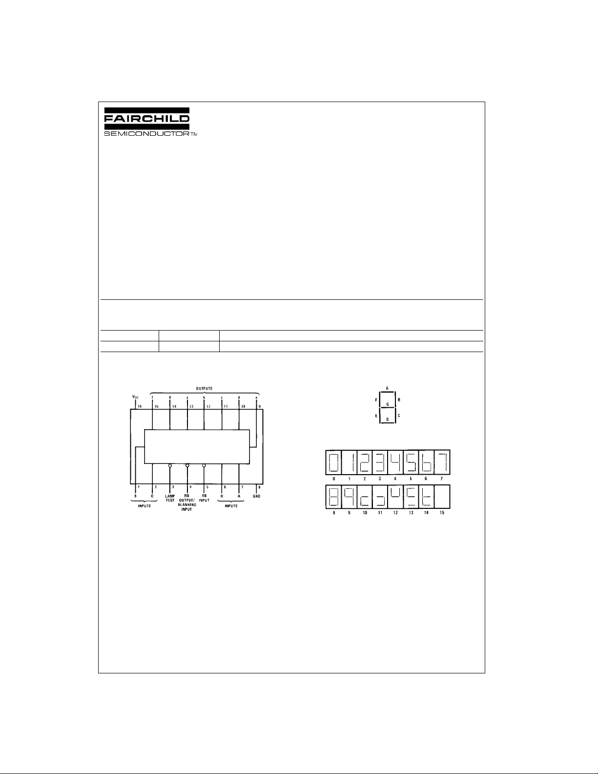
Connection Diagrams
Pin Assignments for DIP
Segment Identification
Numerical Des ignations
and Resultant Displays
Top View
© 1999 Fairchild Semiconductor Corporation DS005883.prf www.fairchildsemi.com

Truth Table
Decimal Inputs Outputs
MM74C48
or BI/RBO Note
Function LT RBI D C B A (Note 1) a b c d e f g
0 HHLLLL H HHHHHHL(Note 2)
1 H X L L L H H L H H L L L L (Note 2)
2HXLLHLHHHLHHLH
3 HXLLHH H HHHHLLH
4HXLHLLHLHHLLHH
5 HXLHLH H HLHHLHH
6 HXLHHL H L LHHHHH
7 HXLHHH H HHHLLLL
8 HXHL L L H HHHHHHH
9 HXHLLH H HHHLLHH
10 H X H L H L H L L L H H L H
11 H X H L H H H L L H H L L H
12 HXHHLL H LHLLLHH
13HXHHLHHHLLHLHH
14 HXHHHL H LL LHHHH
15 HXHHHH H LLLLLLL
BI XXXXXX L LLLLLLL(Note 3)
RBI HLLLLL L LLLLLLL(Note 4)
LT LXXXXX H HHHHHHH(Note 5)
H = HIGH Level
L = LOW Level
X = Irrelevant
Note 1: One BI/RBO is wire-AND logic serving as blanking input (BI) and/or ri pple-blanking output (R BO).
Note 2: The blanking input (BI) must be open when output functions 0–15 are desired. The ripple-blanking input (RBI) must be HIGH, if blanking of a decimal
zero is not desired.
Note 3: When a LOW logi c level is applied directly to the blankin g input (BI), all segment outputs are LOW regardles s of th e level of any other input.
Note 4: When ripp le-bla nkin g input (RBI) a nd in puts A , B, C, and D ar e at a LOW level with the lamp- tes t inpu t HIG H, all se gme nt ou tputs go LOW and the
ripple-blanking out put (RBO) goes to a LOW level (response condition).
Note 5: When the blanking input/ripple-blanking output (BI/RBO) is open and a LOW is applied to the lamp-test inpu t , al l se gm ent outputs are HIGH .
www.fairchildsemi.com 2
 Loading...