

Fairchild Semiconductor KA5M0965QTU Datasheet

KA5M0965Q
Fairchild Power Switch(SPS)
www.fairchildsemi.com
Features
• Precision fixed operating frequency (70kHz)
• Low start-up current(typ. 100uA)
• Pulse by pulse current limiting
• Over Load protection
• Over current protection
• Over voltage protecton (Min. 25V)
• Internal thermal shutdown function
• Under voltage lockout
• Internal high voltage sense FET
• Latch mode
Description
The SPS product family is specially designed for an off-line
SMPS with minimal external components. The SPS consist
of high voltage power SenseFET and current mode PWM
IC. Included PWM controller features integrated fixed frequency oscillator, under voltage lock-out, leading edge
blanking, optimized gate turn-on/turn-off driver, thermal
shutdown protection, over voltage protection, and temperature compensated precision current sources for loopcompensation and fau lt protection circuitry. Compared to discrete
MOSFET and PWM controller or RCC solution, a SPS can
reduce total component count, design size, weight and at the
same time increase efficiency, productivity, and system reliability. It has a basic platform well suited for cost-effective
design in either a flyback converter or a forward converter.
TO-3P-5L
1. DRAIN 2. GND 3. VCC 4. FB 5. S/S
Internal Block Diagram
OVP
++++
27V
-
V
Feed back 4
Soft Start
©2001 Fairchild Semiconductor Corporation
5
7.5V
TSD
(TJ=150℃)
OVP-out
(VCC=27V)
OCL
(VS=1.4V)
CC
++++
-
OVP-out
V
5uA
OLP
Vcc
3
UVLO
Vref
REF
15V/9V
1mA
2.5R
R
5V
OSC
-
++++
Power-on Reset
/Aut o-r e s tart
CLK
LEB
V
OFFSET
INTERNAL
Good Logic
SRQ
S
Q
R
Shutdown
Latch
BIAS
VOLTAGE
CIRCUIT
※
LEB : Leading Edge Blanking
※
OCL : Over Current Limit
LIMIT
V
14V
S
Rsense
Sense
FET
Drain
1
2
GND
Rev.1.0.1
KA5M0965Q
Absolute Maximum Ratings
Characteristic Symbol Value Unit
GS
(2)
(1)
=1MΩ)
C
(3)
=25°C)
Maximum Drain voltage
Drain-Gate voltage (R
Gate-source (GND) voltage
Drain current pulsed
Single pulsed avalanche energy
Continuous drain current (T
Continuous drain current (TC=100°C)
Maximum Supply voltage
Input voltage range
Total power dissipation
Operating ambient temperature
Storage temperature
V
D,MAX
V
DGR
V
I
DM
E
I
I
V
CC,MAX
V
(watt H/S)
P
D
Derating
T
T
STG
GS
AS
D
D
FB
A
650 V
650 V
±30 V
36.0 A
DC
950 mJ
9.0 A
5.8 A
DC
DC
30 V
−0.3 to V
SD
V
170 W
1.33 W/°C
−25 to +85 °C
−55 to +150 °C
Notes:
1. Tj=25°C to 150°C
2. Repetiti ve rating: Pulse width limi ted by maximum junction temp erature
3. L=20mH, V
=50V, RG=27Ω, starting Tj=25°C
DD
2
Electrical Characteristics (SFET part)
(Ta = 25°C unless otherwise specified)
Characteristic Symbol Test condition Min. Typ. Max. Unit
Drain-source breakdown voltage BV
Zero gate voltage drain current I
Static drain-source on resistance
Forward transconductance
(note)
(note)
DSS
DSS
R
DS(ON)VGS
gfs VDS=50V, ID=4.5A 5.0 - - S
Input capacitance Ciss
Reverse transfer capacitance Crss - 25 Turn on delay time td(on) V
Rise time tr - 75 160
Turn off delay time td(off) - 130 270
Fall time tf - 70 150
Total gate charge
(gate-source+gate-drain)
Qg
Gate-source charge Qgs - 8 Gate-drain (Miller) charge Qgd - 22 -
VGS=0V, ID=50µA 650 - - V
VDS=Max., Rating,
V
=0V
GS
=0.8Max., Rating,
V
DS
V
=0V, TC=125°C
GS
--50µA
- - 200 mA
=10V, ID=4.5A - 0.96 1.2 W
V
=0V, VDS=25V,
GS
- 1200 -
f=1MHz
DD
=0.5BV
DSS
, ID=9.0A
-2560
(MOSFET switching
time are essentially
independent of
operating temperature)
V
=10V, ID=9.0A,
GS
V
=0.8BV
DS
DSS
-4560
KA5M0965Q
pFOutput capacitance Coss - 135 -
nS
nC
Note:
Pulse test: Pulse width <
1
S
--- -=
R
300µS, duty < 2%
3

KA5M0965Q
Electrical Charcteristics (SFET part) (Continued)
(Ta = 25°C unless otherwise specified)
Characteristic Symbol Test condition Min. Typ. Max. Unit
UVLO SECTION
Start threshold voltage V
Stop threshold voltage V
START
STOP
After turn on 14 15 16 V
OSCILLATOR SECTION
Initial accuracy F
Frequency change with temperature
(2)
OSC
- −25°C≤Ta≤+85°C-±5 ±10 %
Ta=25°C 616773kHz
Maximum duty cycle Dmax - 74 77 80 %
FEEDBACK SECTION
Feedback source current I
Shutdown Feedback voltage V
FB
SD
Ta=25°C, 0V<Vfb<3V 0.7 0.9 1.1 mA
Vfb>6.5V 6.9 7.5 8.1 V
Shutdown delay current Idelay Ta=25°C, 5V≤Vfb≤V
SOFT START SECTION
Soft Start Voltage V
Soft Start Current I
SS
SS
V
FB
Sync & S/S=GND 0.8 1.0 1.2 mA
CURRENT LIMIT(SELF-PROTECTION)SECTION
Peak Current Limit I
OVER
Max. inductor current 5.28 6.00 6.72 A
PROTECTION SECTION
Thermal shutdown temperature (Tj)
Over voltage protection voltage V
(1)
T
SD
OVP
VCC>24V 25 27 29 V
TOTAL DEVICE SECTION
Start Up current I
Operating supply current (control part only) I
STARTVCC
OP
VCC<28 - 7 12 mA
- 8.4 9 9.6 V
456µA
SD
=2V 4.7 5.0 5.3 V
- 140 160 - °C
=14V - 0.1 0.17 mA
NOTE:
1. These parameters, although guaranteed, are not 100% tested in production
2. These parameters, although guaranteed, are tested in EDS(water test) process
3. These parameters are indicated Inductor current.
4
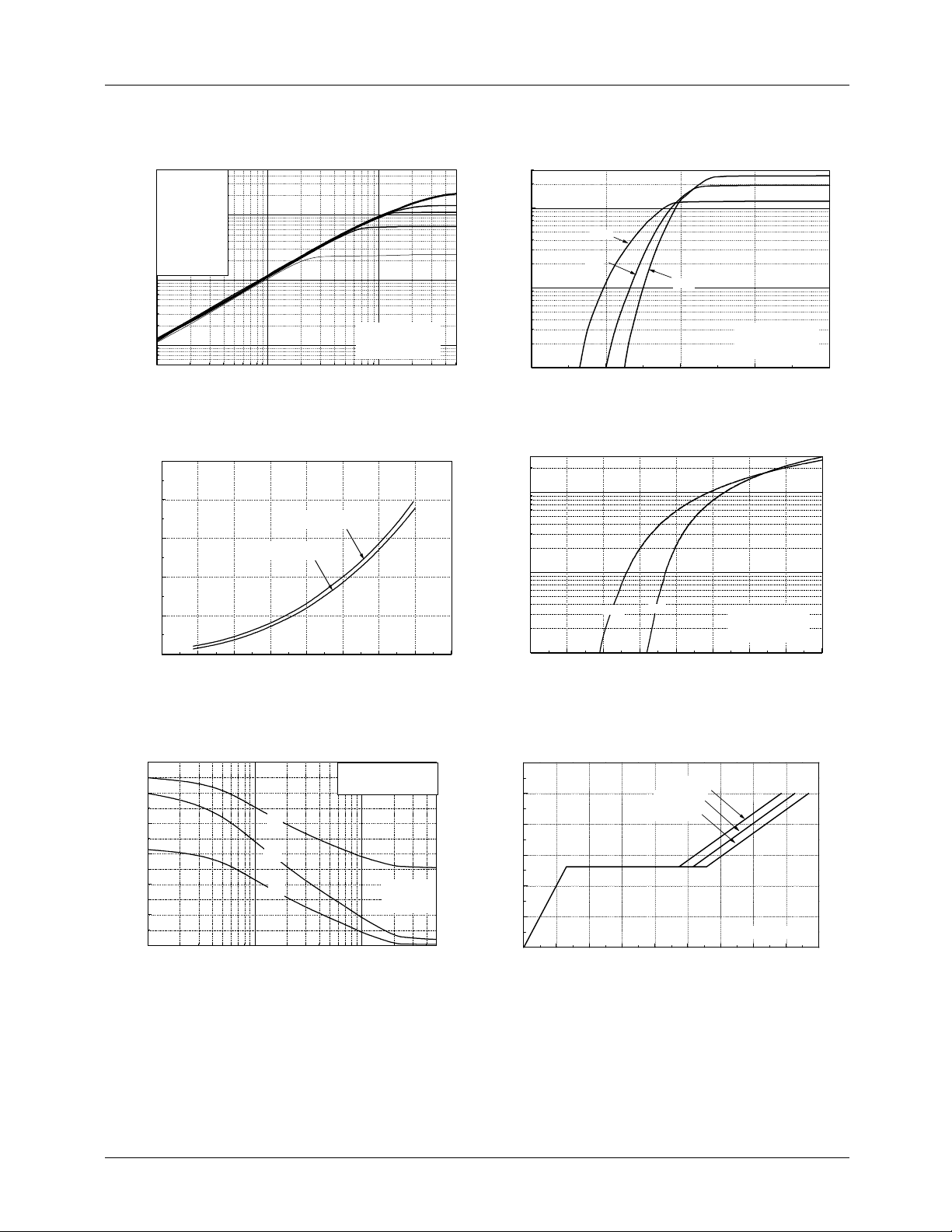
Typical Performance Characteristics
V
GS
Top : 15 V
10 V
8.0 V
1
10
7.5 V
7.0 V
6.5 V
6.0 V
5.5 V
Bottom : 5.0 V
0
10
, Drain Current [A]
D
I
-1
10
-1
10
0
10
VDS , Drain-Source Voltage [V]
Figure 1. Output Characteristics Figure 2. Thansfer Characteristics
1.3
1.2
]
Ω
1.1
, [
DS(on)
R
1.0
VGS = 10V
VGS = 20V
※
Note :
1. 250μs Pulse Test
℃
2. T
= 25
C
1
10
KA5M0965Q
1
10
℃
150
℃
25
℃
0
10
, Drain Current [A]
D
I
-1
10
246810
VGS , Gate-Source Voltage [V]
1
10
0
10
-55
※
Note
1. V
= 50V
DS
2. 250μs Pulse Test
Drain-Source On-Resistance
0.9
0.8
0246810121416
ID , Drain Current [A]
, Reverse Drain Curr ent [A]
DR
I
-1
10
0.0 0.2 0.4 0.6 0.8 1.0 1.2 1.4 1.6
150
VSD , Source-Drain Voltage [V]
℃
25
℃
※
Note :
1. V
= 0V
GS
2. 250μs Pulse Test
Figure 3. On-Resistance vs. Drain Current Figure 4. Source-Drain Diode Forward Voltage
3000
2500
2000
1500
1000
Capacitances [pF]
500
0
-1
10
VDS, Drain-Source Voltage [V]
C
= Cgs + Cgd (Cds = shorted)
iss
C
= Cds + C
oss
gd
C
= C
rss
gd
C
iss
C
oss
※
C
rss
0
10
Note ;
1. V
GS
2. f = 1 MHz
1
10
= 0 V
12
10
8
6
4
, Gate-Source Voltage [V]
2
GS
V
0
0 5 10 15 20 25 30 35 40 45
QG, Total Gate C ha rg e [n C]
VDS = 120V
VDS = 300V
VDS = 480V
※
Note : I
= 8.5 A
D
Figure 5. Capacitance vs. Drain-Source Voltage Figure 6. Gate Charge vs. Gate-Source Voltage
5
 Loading...