Fairchild Semiconductor GTLP36T612 Datasheet

September 2001
Revised July 2002
GTLP36T612
36-Bit LVTTL/GTLP Universal Bus Transceiver
GTLP36T612 36-Bit LVTTL/GTLP Universal Bus Transceiver
General Description
The GTLP36T612 is an 36-bit universal bus transceiver
which provides LVTTL to GTLP sign al level translation. It
allows for transparent, latched and clocked modes of data
transfer. The device provides a high speed interface for
cards operating at LVTTL logic levels and a backplane
operating at GTLP logic levels. High speed backplane
operation is a direct re sult o f GT LP’s redu ced out put s wing
(
< 1V), reduced input threshold levels and output edge rate
control. The edge rate c ontrol mi nimizes b us settl ing time.
GTLP is a Fairchild Semicon ductor derivative of the Gunning Transistor logic (GTL) JEDEC standard JESD8-3.
Fairchild’s GTLP has internal edge-ra te control and is Process, Voltage, and Temperature (PVT) comp ensated. Its
function is similar to BTL or GT L but with different output
levels and receiver thresholds. GTLP output LOW le vel is
less than 0.5V, the output HIGH is 1 .5V and the receiver
threshold is 1.0V.
Features
■ Bidirectional interface between GTLP and LVTTL logic
levels
■ Designed with edge ra te control circuitry to r educe output noise on the GTLP port
■ Partitioned as two 18-Bit transceivers with individual
latch timing and output control
■ V
pin provides extern al supply re ference volta ge for
REF
receiver threshold adjustibility
■ Special PVT compensation circui try to provide consistent performance over var iatio ns of pr ocess, supply voltage and temperature
■ TTL compatible driver and control inputs
■ Designed using Fairchild advanced BiCMOS technology
■ Bushold data inputs on A port to e liminate the need for
external pull-up resistors for unused inputs
■ Power up/down and power off high impedance for live
insertion
■ Open drain on GTLP to support wired-or connection
■ Flow through pinout optimizes PCB layout
■ D-type flip-flop, latch and transparent data paths
■ A Port source/sink
■ B Port sink
■ For more information see AN-5026,
Using BGA Packages
−24mA/+24mA
+50mA
Ordering Code:
Order Number Package Number Package Description
GTLP36T612G
(Note 1)(Note 2)
Note 1: Ordering code “G” indicates Trays.
Note 2: Devices also available in Tape and Reel. Specify by appending th e s uffix let t er “X” to the ordering code.
BGA114A 114-Ball Fine-Pitch Ball Grid Array (FBGA), JEDEC MO-205, 5.5mm Wide
© 2002 Fairchild Semiconductor Corporation DS500590 www.fairchildsemi.com

Truth Table
(Note 3)
Inputs Output Mode
OEAB LEAB CLKAB A B
CEAB
GTLP36T612
X H X X X Z Latched
LLLHXB
LLL LXB
X L H X L L Transparent
XLHXHH
LLL
↑ L L Clocked
LLL ↑ H H storage
HLL XXB
Note 3: A-to-B data flow is shown. B-to-A data flow is similar but uses
OEBA
, LEBA, CLKBA, and CEBA.
Note 4: Output level before the indicated steady state input conditions were
established, provided that CLKAB w as H I GH before LEAB went LOW.
Note 5: Output level befor e the indicated steady-state input conditions
were established.
(Note 4) storage
0
(Note 5) of A data
0
(Note 5) Clock inhibit
0
of A data
Pin Descriptions
Pin Names Description
OEAB
OEBA
CEAB
CEBA
LEAB A-to-B Latch Enable
LEBA B-to-A Latch Enable
V
REF
CLKAB A-to-B Clock (LVTTL Level)
CLKBA B-to-A Clock (LVTTL Level)
A
1–A18
B
1–B18
A-to-B Output Enable
(Active LOW) (LVTTL Level)
B-to-A Output Enable
(Active LOW) (LVTTL Level)
A-to-B Clock/LE Enable
(Active LOW) (LVTTL Level)
B-to-A Clock/LE Enable
(Active LOW) (LVTTL Level)
(Transparent HIGH) (LVTTL Level)
(Transparent HIGH) (LVTTL Level)
GTLP Input Threshold
Reference Voltage
A-to-B Data Inputs or
B-to-A 3-STATE Outputs
B-to-A Data Inputs or
A-to-B Open Drain Outputs
Connection Diagram
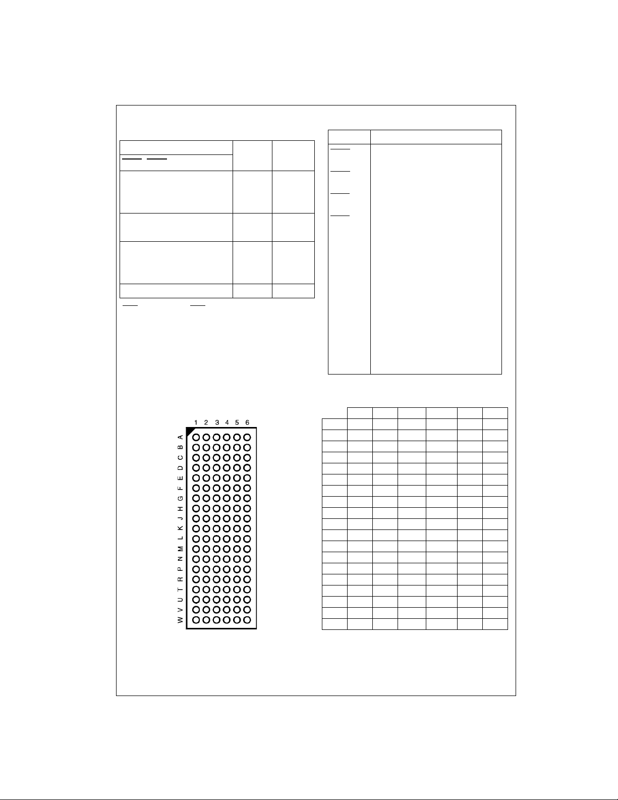
Pin Assignment for FBGA
(Top Thru View)
FBGA Pin Assignments
Number in front of each pin indicate s word.
12 3 4 56
A 1A
B 1A41A31LEAB 1CEAB 1B41B
C 1A61A5V
D 1A81A7GND GND 1B81B
E 1A101A9GND GND 1B101B
F 1A121A11GND GND 1B121B
G 1A141A13V
H 1A161A151OEBA 1CEBA 1B161B
J 1A181A171LEBA 1CLKBA 1B181B
K
L 2A
M 2A42A32LEAB 2CEAB 2B42B
N 2A62A5V
P 2A82A7GND GND 2B82B
R 2A102A9GND GND 2B102B
T 2A122A11GND GND 2B122B
U 2A142A13V
V 2A162A152OEBA 2CEBA 2B162B
W 2A182A172LEBA 2CLKBA 2B182B
1A11OEAB 1 CLKAB 1B21B
2
V
CC
CC
CCVREF
2A12OEAB 2 CLKAB 2B22B
2
V
CC
CC
CCVREF
1B61B
1B141B
2B62B
2B142B
1
3
5
7
9
11
13
15
17
1
3
5
7
9
11
13
15
17
www.fairchildsemi.com 2

Functional Description
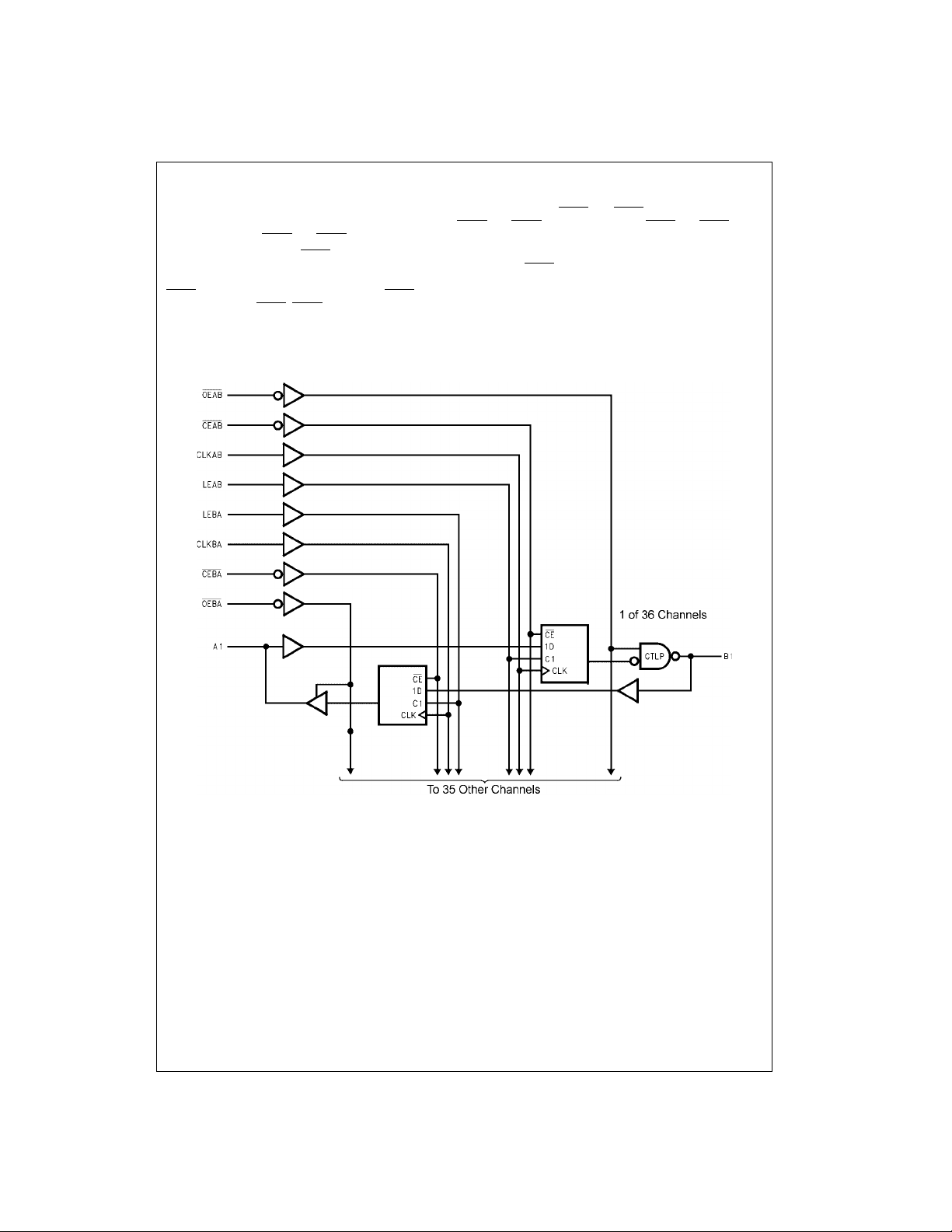
The GTLP36T612 is an 36-bit re giste red tran sceiver con tain ing D-type fl ip-fl op, latch and trans parent modes of op eration
for the data path. Data flow in each d irection is con trolled by the clock enables (CEAB
and LEBA), clock (CLKAB and CLKBA) and output en ables (OEAB
the output enables (OEAB
For A-to-B data flow, when CEAB
and on the HIGH-to-LOW transi tion of LEAB for the latch path. That is , if CEAB
latched regardless as to the state of CLKAB (HIGH or LOW) and if LEAB is HIGH the device is in transparent mode. When
is LOW the outputs are active. W hen OEAB is HIGH the outp uts are HIGH imped ance. The dat a flow of B-to-A is
OEAB
similar except that CEBA
and OEBA) control the 18 bits of data for the A-to-B and B-to-A directions respectively.
is LOW, the device operates on the LOW-to-HIGH transition of CLKAB for the flip-flop
, OEBA, LEBA, and CLKBA are used.
and OEBA). The clock enables (CEAB and CEBA) and
and CEBA), latch enables ( LEAB
is LOW and LEAB is LOW the A data is
Logic Diagram
GTLP36T612
3 www.fairchildsemi.com
 Loading...