

Fairchild Semiconductor GTLP1B151 Datasheet
June 2001
Revised February 2002
GTLP1B151
1-Bit LVTTL/GTLP Transceiver
with Separate LVTTL Port and Feedback Path
GTLP1B151 1-Bit LVTTL/GTLP Transceiver with Separate LVTTL Port and Feedback Path
General Description
The GTLP1B151 is a 1-bit transceiver that provides
LVTTL-to-GTLP signal level translat ion. Individual LVTTL
and GTLP driver enables are also available. The
GTLP1B151 offers separate LVTTL inputs and outputs,
and can provide a feed back path for con trol and diagnostics monitoring.
High-speed backplane operation is a direct result of
GTLP’s reduced output swi ng (
old levels and output edge rate control. The edge rate
control minimizes bus-settling time. GTLP is a Fairchild
Semiconductor derivative of the Gun ning Transistor Logic
(GTL) JEDEC standard JESD8-3.
Fairchild’s GTLP has intern al edge -rate cont rol and i s process, voltage and tem perature compensated. GTLP ’s I/O
structure is similar to GTL and BTL but offers different output levels and receiver threshold. Typical GTLP output voltage levels are: V
= 0.5V, VOH = 1.5V, and V
OL
<1V), reduced inpu t thres h-
= 1V.
REF
Features
■ Separate LVTTL inputs and outputs
■ A feedback path for control and diagnostics monitoring
■ Bidirectional interface between GTLP and LVTTL logic
levels
■ Designed with edge ra te control circuitry to r educe output noise on the GTLP port
■ V
pin provides extern al supply re ference volta ge for
REF
receiver threshold adjustibility
■ Special PVT compensation circui try to provide consistent performance over var iatio ns of pr ocess, supply voltage and temperature
■ TTL compatible driver and control inputs
■ Designed using Fairchild advanced BiCMOS technology
■ Bushold data inputs on A port to e liminate the need for
external pull-up resistors for unused inputs
■ Power up/down and power off high impedance for live
insertion
■ Open drain on GTLP to support wired-or connection
■ Flow through pinout optimizes PCB layout
■ A Port source/sink
■ B Port sink
−24mA / +24mA
+50mA
Ordering Code:
Order Number Package Number Package Description
GTLP1B151M M08A 8-Lead Small Outline Integrated Circuit (SOIC), JEDEC MS-012, 0.150" Narrow
GTLP1B151MX M08A 8-Lead Small Outline Integrated Circuit (SOIC), JEDEC MS-012, 0.150" Narrow
GTLP1B151K8X MAB08A
(Preliminary)
[TUBE]
[TAPE and REEL]
8-Lead US8, JEDEC MO-187, Variation CA 3.1mm Wide
[TAPE and REEL]
© 2002 Fairchild Semiconductor Corporation DS500484 www.fairchildsemi.com
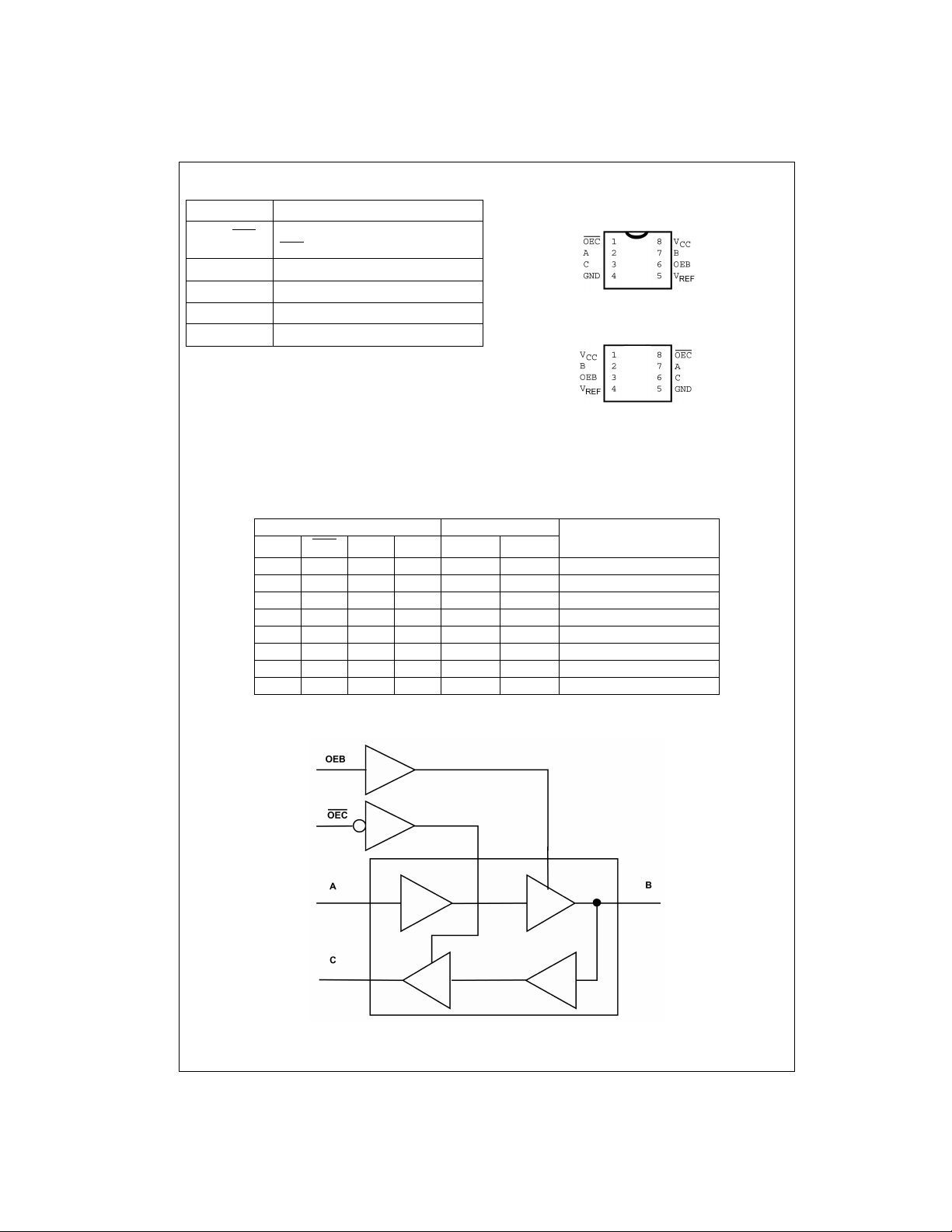
Pin Descriptions Connection Diagrams
Pin Names Description
OEB, OEC
GTLP1B151
, GND, V
V
CC
A A Port LVTTL Input
B B Port GTLP Input/Output
C C Port LVTTL Output
LVTTL Individual Output Enable Controls
(OEC
is Active LOW)
Device Supplies
REF
US8
SOIC
Functional Description
The GTLP1B151 is a 1-bit transceiver that supports GTLP and LVTTL signal levels. Data polarity is non-inverting with separate LVTTL inputs and outputs and there are individual GTLP and LVTTL output enable controls.
Functional Tables
Inputs Outputs
A
OEB OEC
H L L Output L L B Bus Enabled, C Bus Enabled
H L H Output H H B Bus Enabled, C Bus Enabled
H H L Output L Z B Bus Enabled, C Bus Disabled
H H H Output H Z B Bus Enabled, C Bus Disabled
L H L L Z Z B Bus Disabled, C Bus Disabled
L H H H Z Z B Bus Disabled, C Bus Disabled
L L N/A L Z L B Bus Disabled, C Bus Enabled
L L N/A H Z H B Bus Disabled, C Bus Enabled
B
n
B
n
n
C
n
Description
Logic Diagram
www.fairchildsemi.com 2
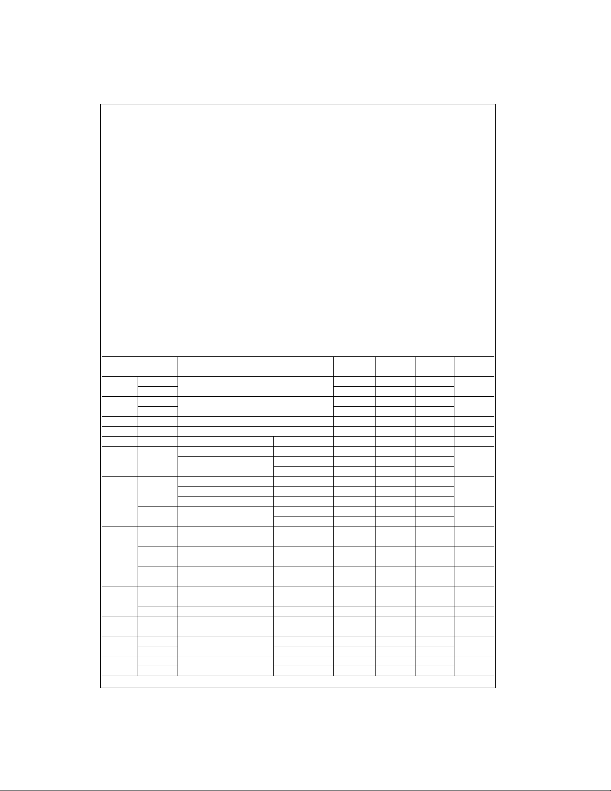
Absolute Maximum Ratings(Note 1) Recommended Operating
Supply Voltage (VCC) −0.5V to +4.6V
DC Input Voltage (V
DC Output Voltage (V
Outputs 3-STATE
Outputs Active (Note 2)
) −0.5V to +4.6V
I
)
O
−0.5V to +4.6V
−0.5V to +4.6V
DC Output Sink Current into
C Port I
OL
48 mA
DC Output Source Current from
C Port I
OH
−48 mA
DC Output Sink Current into
B Port in the LOW State, I
DC Input Diode Current (I
< 0V −50 mA
V
I
DC Output Diode Current (I
V
< 0V −50 mA
O
OL
)
IK
)
OK
ESD Rating
Storage Temperature (T
) −65°C to +150°C
STG
100 mA
>2000V
Conditions
Supply Voltage V
Bus Termination Voltage (V
GTLP 1.47V to 1.53V
V
REF
Input Voltage (V
on A Port and Control Pins 0.0V to V
HIGH Level Output Current (IOH)
C Port
LOW Level Output Current (I
C Port
B Port
Operating Temperature (T
Note 1: Absolute Maximum Ratings are those values beyond which the
safety of the device can not be gu arant eed. The de vice sh ould no t be oper-
ated at these limits. The parametric values defined in the “Electrical Characteristics” table are not guarant eed at the ab solute max imum ratin g. The
“Recommended Operating Con ditions” table will define the conditions for
actual device opera tion.
Absolute Maximum Rating must be observed.
Note 2: I
O
CC
)
I
)
TT
)
OL
) −40°C to +85°C
A
DC Electrical Characteristics
Over Recommended Operating Free-Air Temperature Range, V
Symbol Test Conditio ns
V
IH
V
IL
V
REF
V
TT
V
IK
V
OH
V
OL
I
I
I
OFF
I
I (HOLD)
I
OZH
I
OZL
B Port V
Others 2.0
B Port 0.0 V
Others 0.8
B Port 0.7V 1.0 1.3V V
B Port V
C Port VCC = Min to Max (Note 4) IOH = −100 µAV
C Port VCC = Min to Max (Note 4) IOL = 100 µA0.2
B Port VCC = 3.15V IOL = 40 mA 0.4
Control Pins VCC = 3.45V VI = 3.45V 5
A Port VCC = 3.45V VI = 3.45V 10
B Port VCC = 3.45V VI = 3.45 5
A or C Ports, VCC = 0V
Control Pins
B Port VCC = 0V
A Port VCC = 3.15V VI = 0.8V 75
C Port VCC = 3.45V VO = 3.45V 10
B Port VO = 3.45V 5
C Port VCC = 3.45V VO = 0V −10
B Port VO = 0.0V −5
VCC = 3.15V II = −18 mA −1.2 V
= 3.15V IOH = −8 mA 2.4
CC
= 3.15V IOL = 24mA 0.5
V
CC
= 1.0V (unless otherwise noted).
REF
= -24mA 2.2
I
OH
IOL = 50 mA 0.55
VI = 0V −5
VI = 0V −10
VI = 0 −5
or VO = 0 to 3.45V 30 µA
I
or VO = 0 to 3.45V 30 µA
I
VI = 2.0V −75
Min Typ Max
+ 0.05 V
REF
+ 50 mV 1.5 V
REF
–0.2
CC
(Note 3)
REF
3.15V to 3.45V
0.98V to 1.02V
−24 mA
+24 mA
+50 mA
TT
− 0.05
CC
GTLP1B151
CC
Units
V
V
V
VV
VVCC = 3.15V IOL = 8 mA 0.4
V
µA
µA
µA
µA
µA
µA
3 www.fairchildsemi.com
 Loading...