Fairchild Semiconductor DM74LS174SJ, DM74LS174N, DM74LS174MX, DM74LS174M, DM74LS174CW Datasheet
...
© 2000 Fairchild Semiconductor Corporation DS006404 www.fairchildsemi.com
August 1992
Revised April 2000
DM74LS174 • DM74LS175 Hex/Quad D-Type Flip-Flops with Clear
DM74LS174 • DM74LS175
Hex/Quad D-Type Flip-Flops with Clear
General Description
These positive-edge-triggered flip-flops utilize TTL circuitry
to implement D-type flip-flop logic. All have a direct clear
input, and the quad (175) ver sions fea ture comp lementary
outputs from each flip-flop.
Information at the D in puts meeting the setup ti m e req uir ements is transferred t o the Q output s on the positi ve-goi ng
edge of the clock pulse. Clock trigger ing occ urs a t a par ticular voltage level and is not directly related to the transition
time of the positive-goi ng pulse . When the clock in put is at
either the HIGH or LOW le vel, the D input signal has no
effect at the output.
Features
■ DM74LS174 contains six flip-flops with single-rail
outputs
■ DM74LS175 contains four flip-flops with double-rail
outputs
■ Buffered clock and direct clear inputs
■ Individual data input to each flip-flop
■ Applications include:
Buffer/storage registers
Shift registers
Pattern generators
■ Typical clock frequency 40 MHz
■ Typical power dissipation per flip-flop 14 mW
Ordering Code:
Devices also availab le in Tape and Reel. Specify by appending th e s uffix let t er “X” to the ordering code.
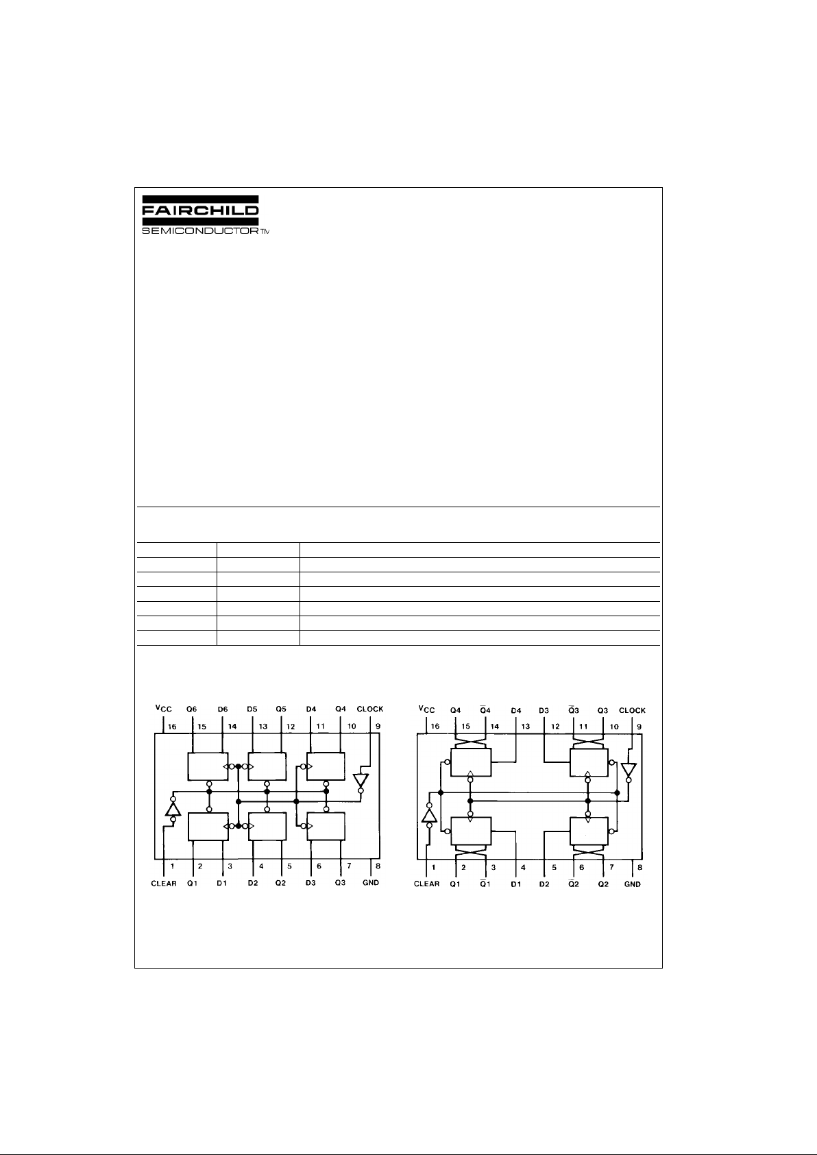
Connection Diagrams
DM74LS174 DM74LS175
Order Number Package Number Package Description
DM74LS174M M16A 16-Lead Small Outline Integrated Circuit (SOIC), JEDEC MS-012, 0.15 0 Narrow
DM74LS174SJ M16D 16-Lead Small Outline Package (SOP), EIAJ TYPE II, 5.3mm Wide
DM74LS174N N16E 16-Lead Plastic Dual-In-Line Package (PDIP), JEDEC MS-001, 0.300 Wide
DM74LS175M M16A 16-Lead Small Outline Integrated Circuit (SOIC), JEDEC MS-012, 0.15 0 Narrow
DM74LS175SJ M16D 16-Lead Small Outline Package (SOP), EIAJ TYPE II, 5.3mm Wide
DM74LS175N N16E 16-Lead Plastic Dual-In-Line Package (PDIP), JEDEC MS-001, 0.300 Wide

www.fairchildsemi.com 2
DM74LS174 • DM74LS175
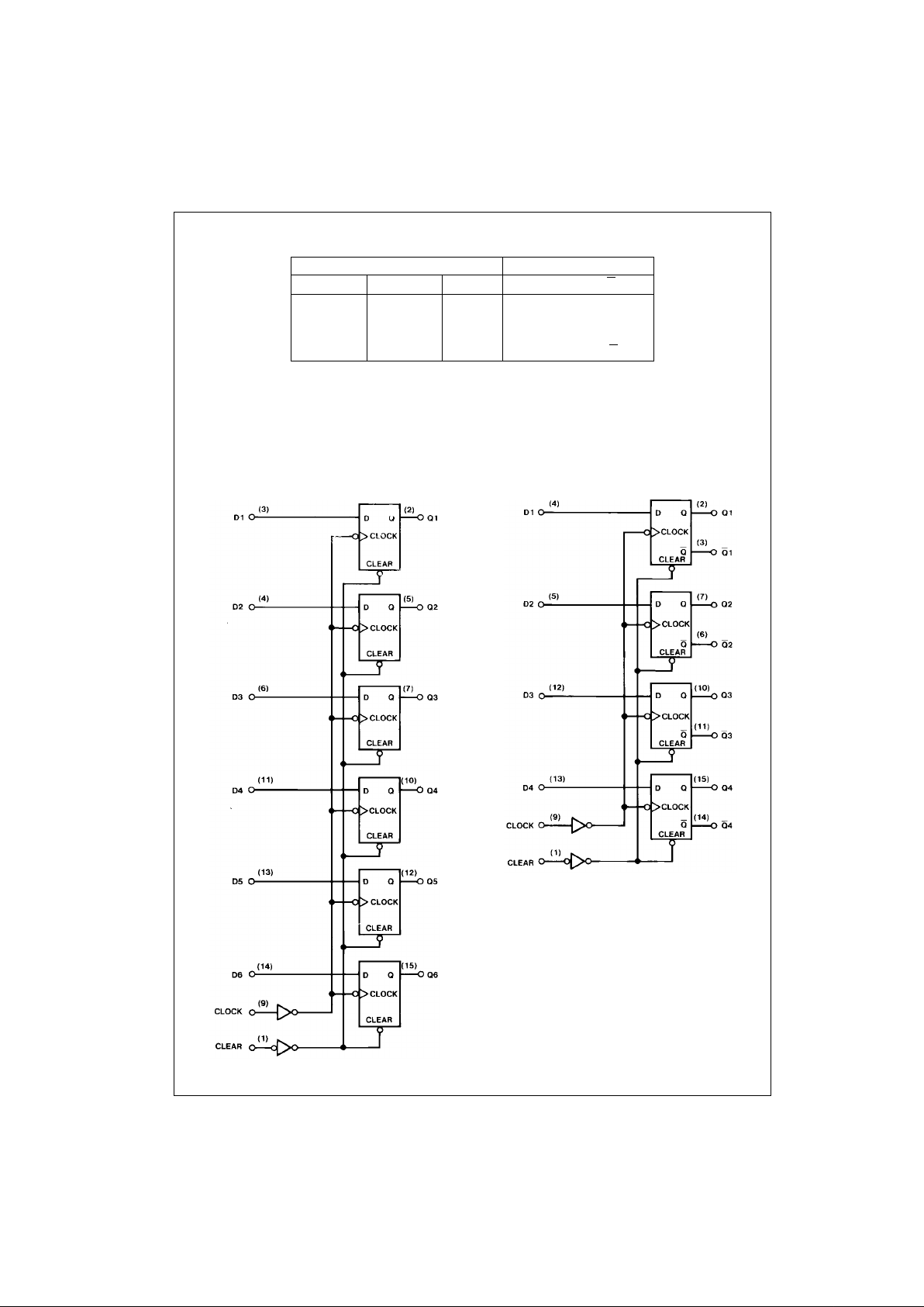
Function Table
(Each Flip-Flop)
H = HIGH Level (steady state)
L = LOW Level (steady state)
X = Don’t Care
↑ = Transition from LOW-to-HIGH lev el
Q
0
= The level of Q befo re t he indicated steady-state input conditions we re established.
† = DM74LS175 only
Logic Diagrams
DM74LS174 DM74LS175
Inputs Outputs
Clear Clock D Q Q
†
LXXLH
H ↑ HH L
H ↑ LL H
HLXQ
0
Q
0

3 www.fairchildsemi.com
DM74LS174 • DM74LS175
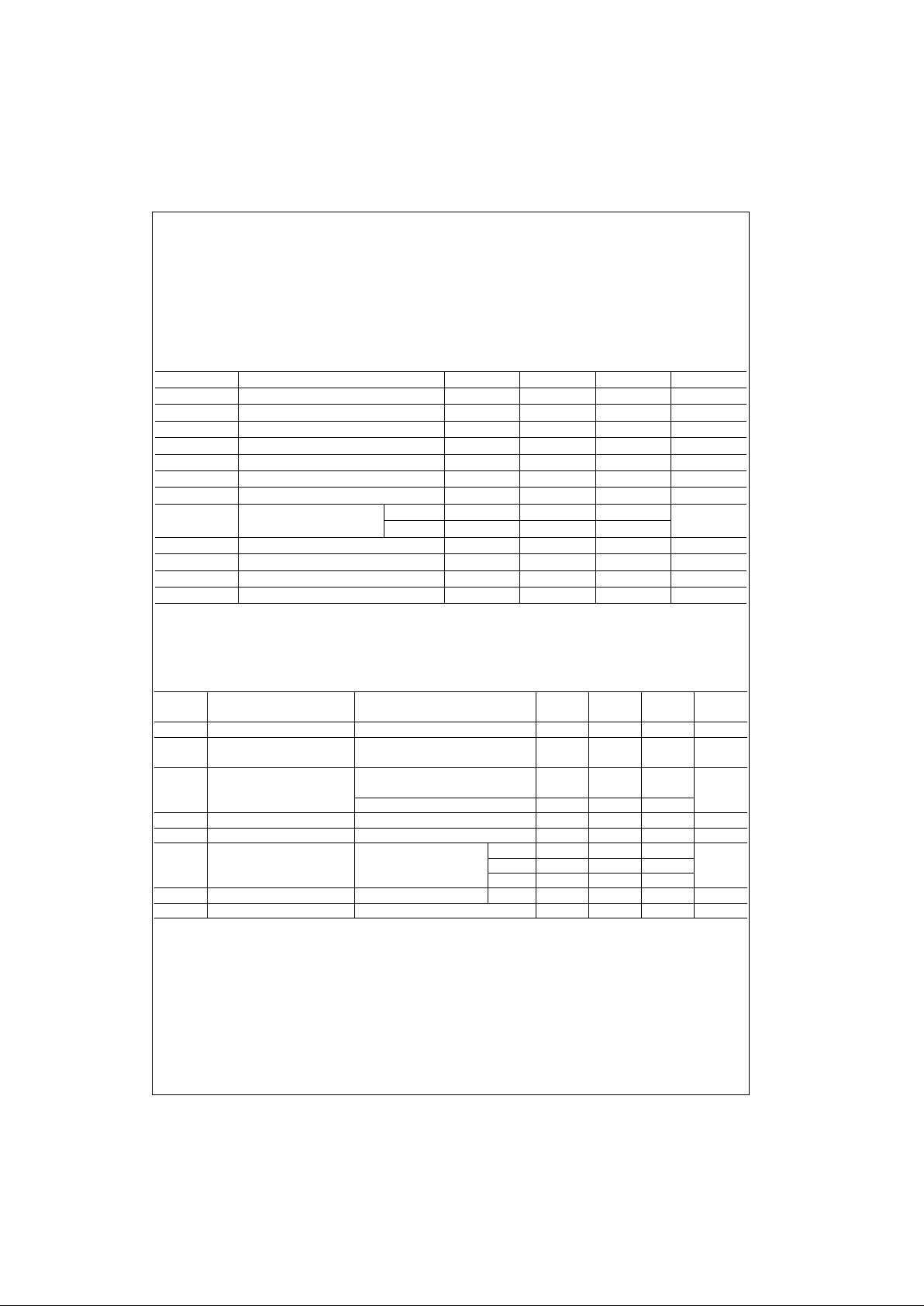
Absolute Maximum Ratings(Note 1)
Note 1: The “Absolute Maximum Ratings ” are those val ues beyond w hich
the safety of the device cannot be guaranteed. The device should not be
operated at these limits. The parametric values defined in the Electrical
Characteristics tables are not guaranteed at the absolute maximum ratings.
The “Recommend ed O peratin g Cond itions” t able w ill defin e the condition s
for actual device operation.
DM74LS174 Recommended Operating Conditions
Note 2: CL = 15 pF, RL = 2 kΩ, TA = 25°C and VCC = 5V.
Note 3: C
L
= 50 pF, RL = 2 kΩ, TA = 25°C and VCC = 5V.
Note 4: T
A
= 25°C and VCC = 5V.
DM74LS174 Electrical Characteristics
over recommended operating free air temperature range (unless otherwise noted)
Note 5: All typicals are at VCC = 5V, TA = 25°C.
Note 6: Not more than one output should be shorted at a time, and the duration should not exceed one second.
Note 7: With all output s O PEN and 4.5V applied t o all data and clear inputs, I
CC
is measured after a m om entary ground, then 4. 5V applied to the clock .
Supply Voltage 7V
Input Voltage 7V
Operating Free Air Temperature Range 0°C to +70°C
Storage Temperature Range −65°C to +150°C
Symbol Parameter Min Nom Max Units
V
CC
Supply Voltage 4.75 5 5.25 V
V
IH
HIGH Level Input Voltage 2 V
V
IL
LOW Level Input Voltage 0.8 V
I
OH
HIGH Level Output Current −0.4 mA
I
OL
LOW Level Output Current 8 mA
f
CLK
Clock Frequency (Note 2) 0 30 MHz
f
CLK
Clock Frequency (Note 3) 0 25 MHz
t
W
Pulse Width Clock 20
ns
(Note 4) Clear 20
t
SU
Data Setup Time (Note 4) 20 ns
t
H
Data Hold Time (Note 4) 0 ns
t
REL
Clear Release Time (Note 4) 25 ns
T
A
Free Air Operating Temperature 0 70 °C
Symbol Parameter Conditions Min
Typ
Max Units
(Note 5)
V
I
Input Clamp Voltage VCC = Min, II = −18 mA −1.5 V
V
OH
HIGH Level VCC = Min, IOH = Max
2.7 3.4 V
Output Voltage VIL = Max, VIH = Min
V
OL
LOW Level VCC = Min, IOL = Max
0.35 0.5
Output Voltage VIL = Max, VIH = Min V
IOL = 4 mA, VCC = Min 0.25 0.4
I
I
Input Current @ Max Input Voltage VCC = Max, VI = 7V 0.1 mA
I
IH
HIGH Level Input Current VCC = Max, VI = 2.7V 20 µA
I
IL
LOW Level VCC = Max Clock −0.4
Input Current VI = 0.4V Clear −0.4 mA
Data −0.36
I
OS
Short Circuit Output Current VCC = Max (Note 6) −20 −100 mA
I
CC
Supply Current VCC = Max (Note 7) 16 26 mA
 Loading...