Fairchild Semiconductor DM74LS169AN, DM74LS169AMX, DM74LS169AM, DM74LS169ACW Datasheet

© 2000 Fairchild Semiconductor Corporation DS006401 www.fairchildsemi.com
August 1986
Revised April 2000
DM74LS169A Synchronous 4-Bit Up/Down Binary Counter
DM74LS169A
Synchronous 4-Bit Up/Down Binary Counter
General Description
This synchronous pre settable counter f eatures an inter nal
carry look-ahead for cascading in high-speed counting
applications. Synchronou s operation is provided by ha ving
all flip-flops clocked simult aneously, so that the outputs all
change at the same time when so instr ucted by the coun tenable inputs and int ernal gating. This m ode of operation
helps eliminate the output counting spikes that are normally associated with asynchronous (ripple clock)
counters. A buffered clock i nput triggers the four ma sterslave flip-flops on the rising edge of the clock waveform.
This counter is fully programmable; that is, the outputs may
each be preset either HIG H or LOW. The load input circuitry allows loading with the carry-enable output of cascaded counters. As loading is synchr onous, setting up a
low level at the load inp ut disab l es the cou nte r a nd cau ses
the outputs to agre e with the data inputs after the next
clock pulse.
The carry look-ahead cir cuitry permits casca ding counters
for n-bit synchronous applications without additional gating.
Both count-enable inputs (P
and T) must be LOW to count.
The direction of the co unt is determ ined b y the leve l of t he
UP/DOWN input. When the input is HIGH, the counter
counts UP; when LOW, it counts DOWN. Input T
is fed for-
ward to enable the ca rry outputs. The carry output thus
enabled will produce a low-level output pulse with a duration approximately e qual to th e high portion o f the Q
A
out-
put when counting UP, and approximately equ al to the low
portion of the Q
A
output when counting DOWN. This low-
level overflow carry pulse can be used to en able successively cascaded stages . Transitions at the enable P
or T
inputs are allowed regardless of the level of the clock input.
All inputs are diode clamped to minimize transmission -line
effects, thereby simplifying system design.
This counter features a fully independent clock circuit.
Changes at control inputs ( enable P
, enable T, load, UP/
DOWN), which modify the ope rating mode, hav e no effect
until clocking occur s. The function o f the co unter ( whether
enabled, disabled, loading, or counting) will be dictated
solely by the conditions m eeting the sta ble setup and hold
times.
Features
■ Fully synchronous operation for counting and
programming.
■ Internal look-ahead for fast counting.
■ Carry out put for n-bi t cascading.
■ Fully independent clock circuit
Ordering Code:
Devices also availab le in Tape and Reel. Specify by appending th e s uffix let t er “X” to the ordering code.
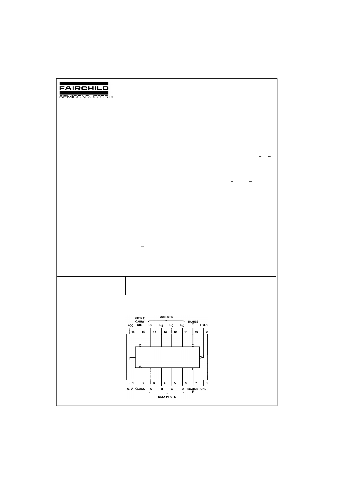
Connection Diagram
Order Number Package Number Package Description
DM74LS169AM M16A 16-Lead Small Outline Integrated Circuit (SOIC), JEDEC MS-012, 0.150 Narrow
DM74LS169AN N16E 16-Lead Plastic Dual-In-Line Package (PDIP), JEDEC MS-001, 0.300 Wide

www.fairchildsemi.com 2
DM74LS169A
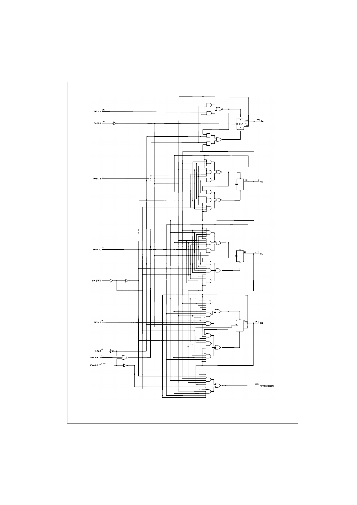
Logic Diagram

3 www.fairchildsemi.com
DM74LS169A
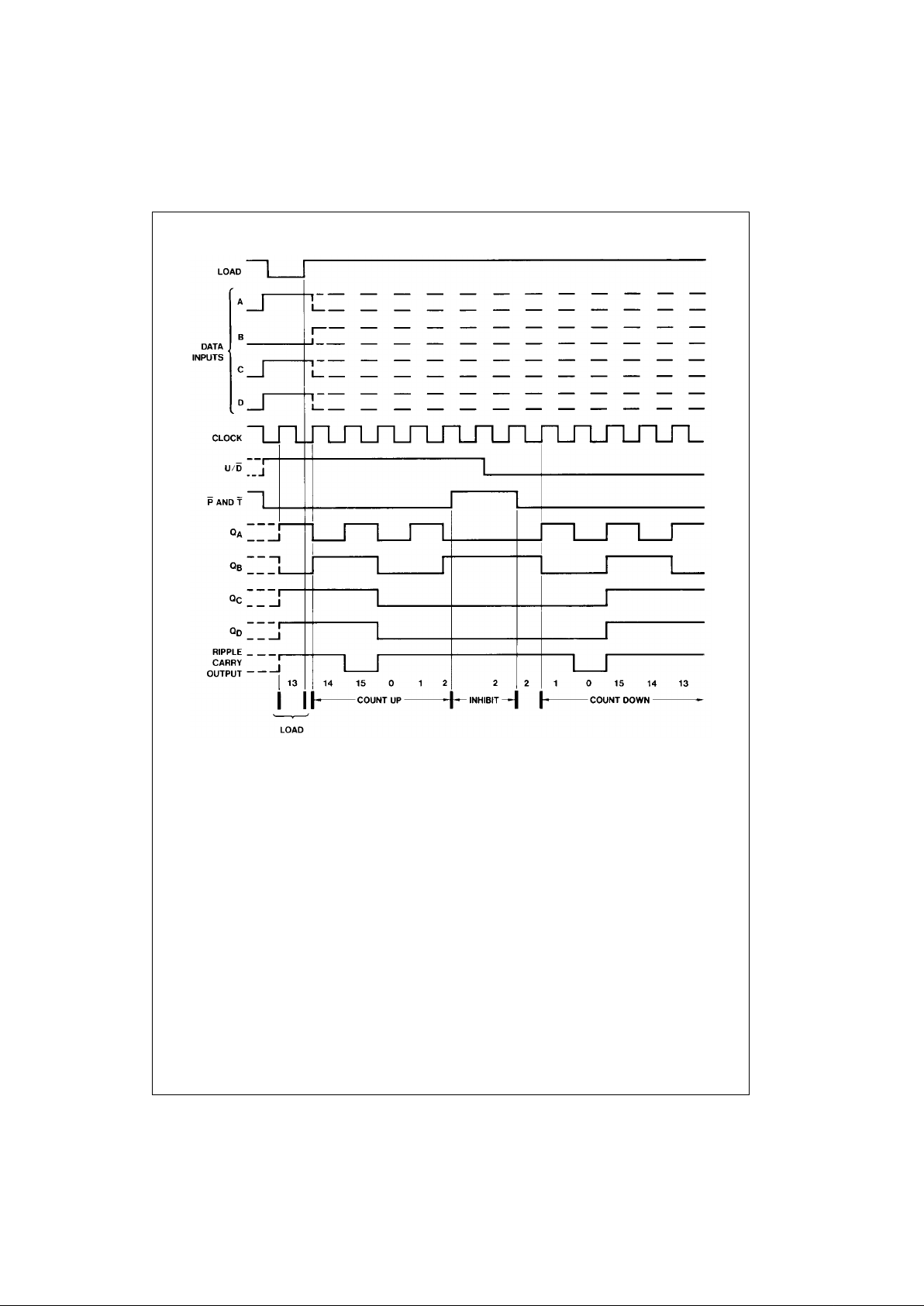
Timing Diagram
Typical Load, Count, and Inhibit Sequences
 Loading...