

Fairchild Semiconductor DM74LS166WM, DM74LS166N, DM74LS166MX, DM74LS166M, DM74LS166WMX Datasheet
© 2000 Fairchild Semiconductor Corporation DS006400 www.fairchildsemi.com
August 1986
Revised March 2000
DM74LS166 8-Bit Parallel-In/Serial-Out Shift Register
DM74LS166
8-Bit Parallel-In/Serial-Out Shift Register
General Description
These parallel-in or serial-in, serial-out shift registers feature gated clock inputs and an ov erriding clear input. All
inputs are buffered to l ower the d rive requirem ents to one
normalized load, and input clamping diodes minimize
switching transients to simplify system design. The load
mode is established by the shift/load input. When HIGH,
this input enables the serial data input and couples the
eight flip-flops for serial shifting with each clock pulse.
When LOW, the parallel (broadside) data inputs are
enabled and synchronou s load ing occurs on the next clock
pulse. During parallel loa ding, serial data flow i s inhibited.
Clocking is accomplished on the LOW-to-HIGH level edge
of the clock pulse through a two-input NOR gate, permitting
one input to be used as a clock-enable or clock-inhibit function. Holding either of the clock inpu ts HIGH inhibits clocking; holding either LOW e na bles t he other clock input. This
allows the system clock to be free running, and the register
can be stopped on c ommand with the other clock in put.
The clock-inhibit input shou ld be changed to the high level
only while the clock input is HIGH. A buffered, direct cl ear
input overrides all other inputs, including the clock, and
sets all flip-flops to zero.
Ordering Code:
Devices also availab le in Tape and Reel. Specify by appending th e s uffix let t er “X” to the ordering code.
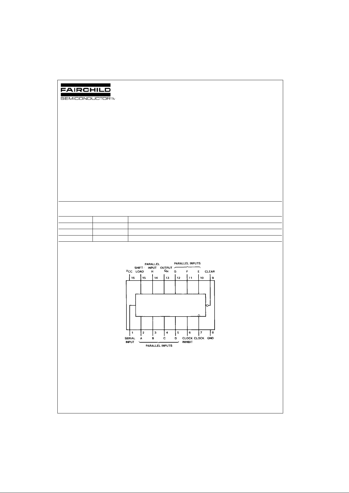
Connection Diagram
Order Number Package Number Package Description
DM74LS166M M16A 16-Lead Small Outline Integrated Circuit (SOIC), JED EC MS-012, 0.150 Narrow
DM74LS166WM M16B 16-Lead Small Outline Intergrated Circuit (SOIC), JEDEC MS-013, 0.300 Wide
DM74LS166N N16E 16-Lead Plastic Dual-In-Line Package (PDIP), JEDEC MS-001, 0.300 Wide
www.fairchildsemi.com 2
DM74LS166
Function Table
H = HIGH Level (steady state)
L = LOW Level (steady state)
X = Don’t Care (any input, including transitions)
↑ = Transition from LOW-to-HIGH lev el
a…h = The level of steady-state input at inputs A through H, respectively
Q
A0
, QB0, QH0 = The level of QA, QB, QH, respectively, before the indicated steady-state input co nditions were establis hed
Q
An
, QGn, = The level of QA, QG, respectively, before the most recent ↑ transition of the clock
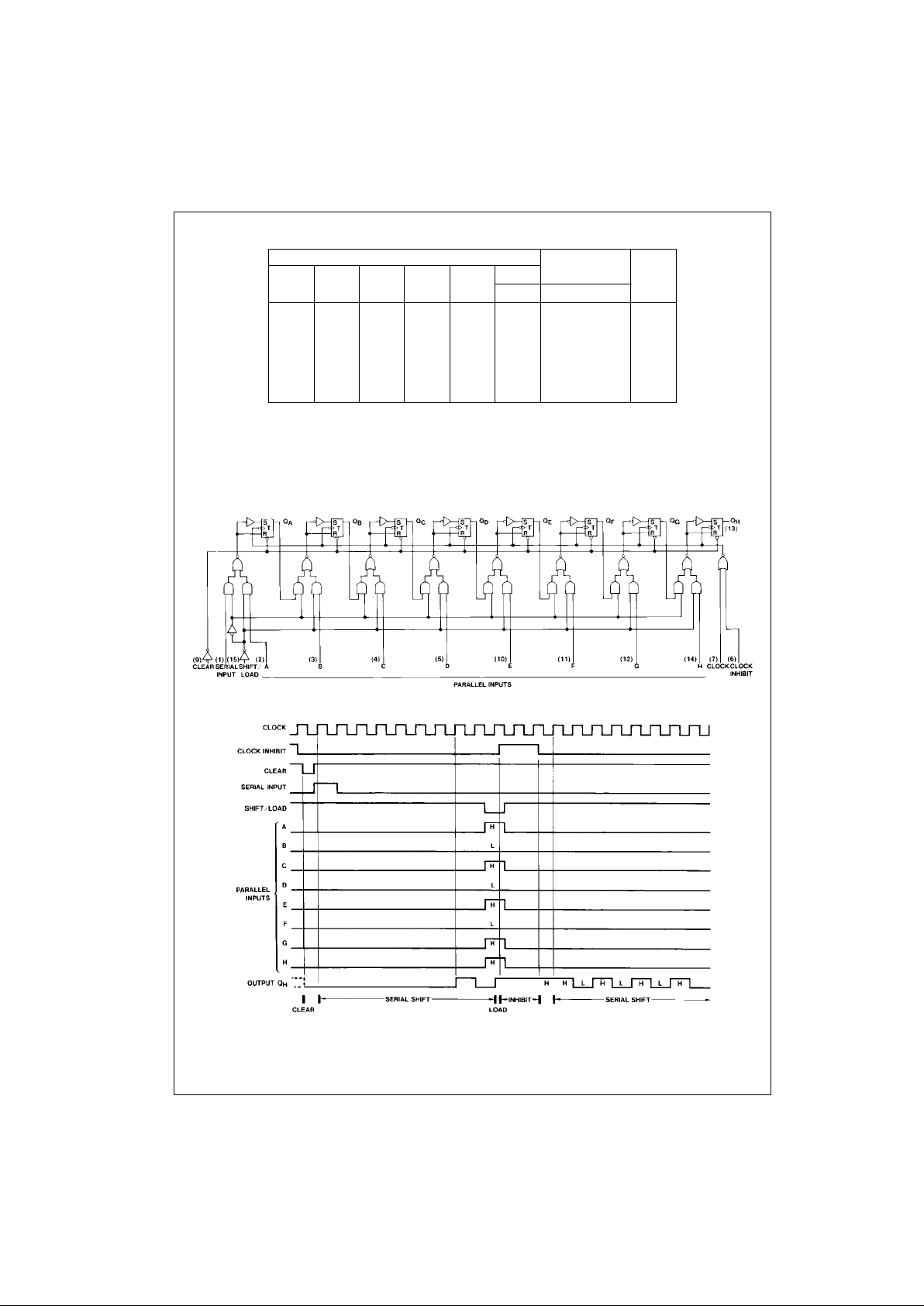
Logic Diagram
Timing Diagram
Typical Clear, Shift, Load, Inhibit and Shift Sequences
Inputs Internal Output
Clear
Shift/ Clock
Clock Serial
Parallel Outputs Q
H
Load Inhibit
A…H Q
A
Q
B
LXXXXXLLL
HXLLXXQ
A0
Q
B0
Q
H0
HLL↑ X a…habh
HHL ↑ HXHQ
An
Q
Gn
HHL ↑ LXLQAnQ
Gn
HXH↑ XXQA0Q
B0
Q
H0
 Loading...