Fairchild Semiconductor DM74LS165WMX, DM74LS165WM, DM74LS165N, DM74LS165MX, DM74LS165M Datasheet
...
© 2000 Fairchild Semiconductor Corporation DS006399 www.fairchildsemi.com
August 1986
Revised March 2000
DM74LS165 8-Bit Parallel In/Serial Output Shift Registers
DM74LS165
8-Bit Parallel In/Serial Output Shift Registers
General Description
This device is an 8-bit se rial sh ift regi ster wh ich shif ts data
in the direction of Q
A
toward QH when clocked. Parallel-in
access is made available by eight individual direct data
inputs, which are enabled by a low level at the shift/load
input. These register s also feature gat ed clock inputs and
complementary outputs from the eighth bit.
Clocking is accomplished through a 2-input NOR gate, permitting one input to be used as a clock-inhibit function.
Holding either of the clock inputs HIGH inhibits clocking,
and holding either clock input LOW with the load input
HIGH enables the other clock input. Th e clock-inhibit input
should be changed to the high level onl y while the clock
input is HIGH. Parallel loading is inhibited as lo ng as the
load input is HIGH. D ata at the parallel in puts are loaded
directly into the register on a HIGH-to-LOW transition of the
shift/load input, regardless of th e logic levels on the clock,
clock inhibit, or serial inputs.
Features
■ Complementary outputs
■ Direct overriding (data) inputs
■ Gated clock inputs
■ Parallel-to-serial data conversion
■ Typical frequency 35 MHz
■ Typical power dissipation 105 mW
Ordering Code:
Devices also availab le in Tape and Reel. Specify by appending th e s uffix let t er “X” to the ordering code.
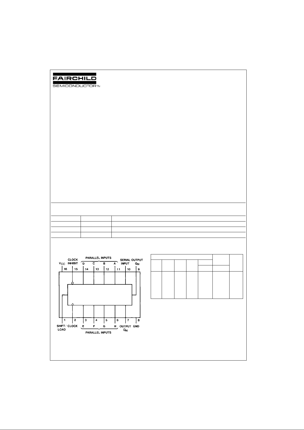
Connection Diagram Function Table
H = HIGH Level (steady state)
L = LOW Level (steady state)
X = Don't Care (any input, including transitions)
↑ = Transition from LOW-to-HIGH level
a...h = The level of steady-state input at inputs A through H, respectively.
Q
A0
, QB0, QH0 = The level of QA, QB, or QH, respectively, before the
indicated steady-s ta t e input conditions were es t ablished.
Q
An
, QGn = The level of QA or QG, respectively, before the most recent
↑ transition of the clock.
Order Number Package Number Package Description
DM74LS165M M16A 16-Lead Small Outline Integrated Circuit (SOIC), JEDEC MS-012, 0.150 Narrow
DM74LS165WM M16B 16-Lead Small Outline Intergrated Circuit (SOIC), JEDEC MS-013, 0.300 Wide
DM74LS165N N16E 16-Lead Plastic Dual-In-Line Package (PDIP), JEDEC MS-001, 0.300 Wide
Inputs Internal
Shift/ Clock Clock Serial Parallel Outputs Output
Load Inhibit A...H
Q
AQBQH
L X X X a...h a b h
HL LX XQ
A0QB0QH0
HL ↑ HXHQAnQ
Gn
HL ↑ LXLQAnQ
Gn
HHXX XQA0QB0Q
H0

www.fairchildsemi.com 2
DM74LS165
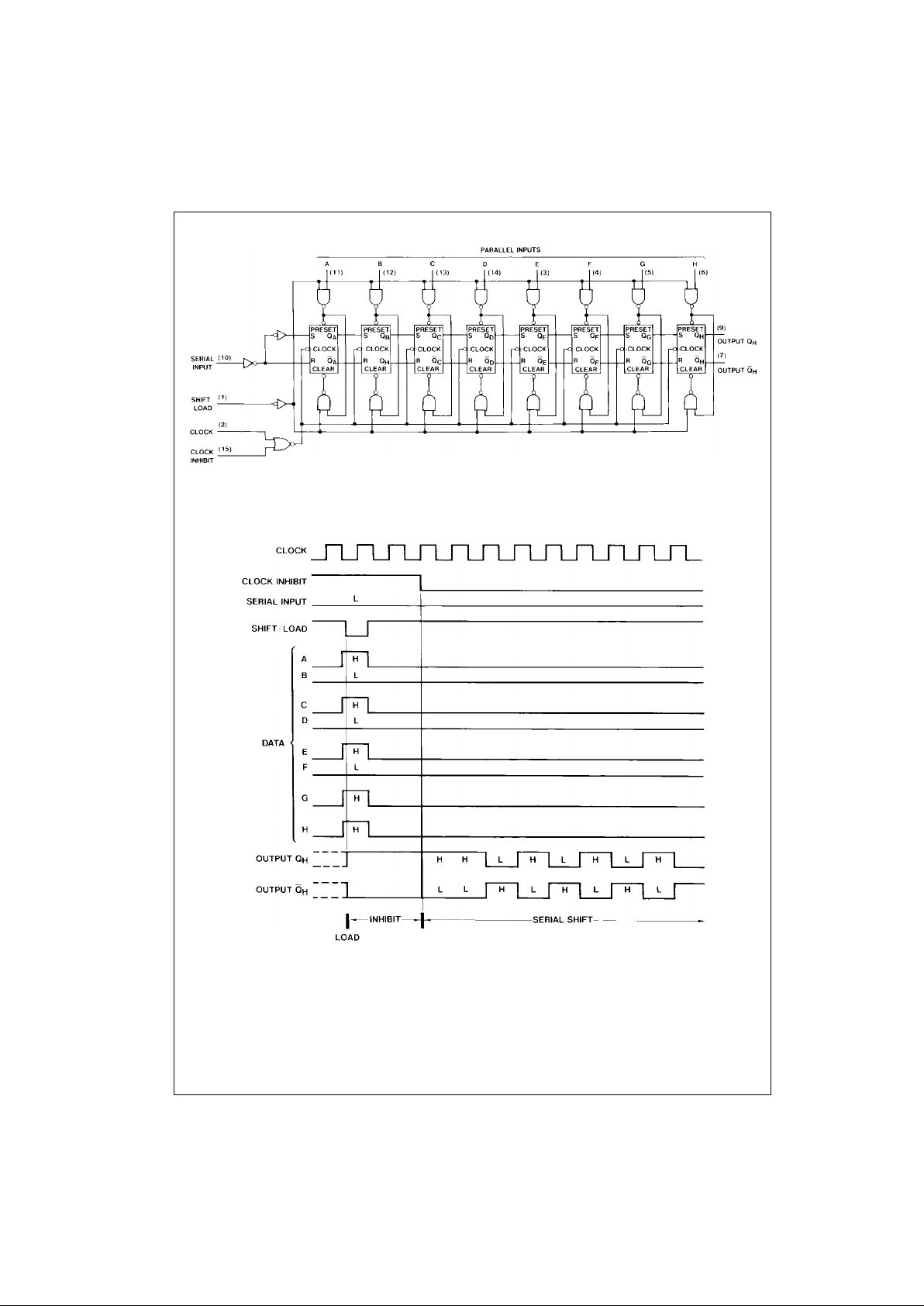
Logic Diagram
Timing Diagram
Typical Shift, Load, and Inhibit Sequences
 Loading...