Fairchild Semiconductor DM74LS164N, DM74LS164MX, DM74LS164M, DM74LS164CW Datasheet

© 2000 Fairchild Semiconductor Corporation DS006398 www.fairchildsemi.com
August 1986
Revised April 2000
DM74LS164 8-Bit Serial In/Parallel Out Shift Register
DM74LS164
8-Bit Serial In/Parallel Out Shift Register
General Description
These 8-bit shift registe rs feature gated serial inpu ts and
an asynchronous clear. A low logic level at either input
inhibits entry of the new data, and resets the first flip-flop to
the low level at t he next clock pulse , thus providing com plete control over incoming data. A high logic level on
either input enables the other input, which will then dete rmine the state of the first flip-flo p. Data at the serial inputs
may be changed while th e cloc k is HIG H or LOW, but only
information meeting th e setup and ho ld time require ments
will be entered. Clocking occurs on the LOW-to-HIGH level
transition of the clock input. All inputs are diode-clamped to
minimize transmission-line effects.
Features
■ Gated (enable/disable) serial inputs
■ Fully buffered clock and serial inputs
■ Asynchronous clear
■ Typical clock frequency 36 MHz
■ Typical power dissipation 80 mW
Ordering Code:
Devices also availab le in Tape and Reel. Specify by appending th e s uffix let t er “X” to the ordering code.
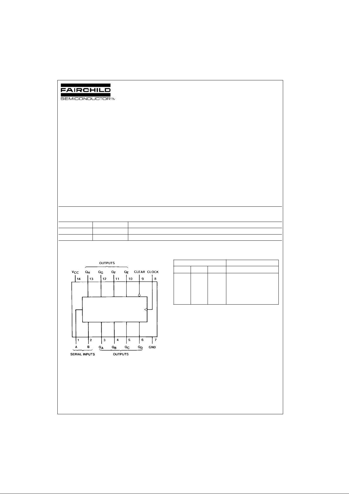
Connection Diagram Function Table
H = HIGH Level (steady state)
L = LOW Level (steady state)
X = Don't Care (any input, including transitions)
↑ = Transition from LOW-to-HIGH level
Q
A0
, QB0, QH0 = The level of QA, QB, or QH, respectively, before the
indicated steady-s t at e input conditions we re es t ablished.
Q
An
, QGn = The level of QA or QG before the most recent ↑ transition of the
clock; indicates a one-bit shift.
Order Number Package Number Package Description
DM74LS164M M14A 14-Lead Small Outline Integrated Circuit (SOIC), JEDEC MS-120, 0.150 Narrow
DM74LS164N N14A 14-Lead Plastic Dual-In-Line Package (PDIP), JEDEC MS-001, 0.300 Wide
Inputs Outputs
Clear Clock A B
Q
AQB
...
Q
H
LXXXLL...L
HLXXQ
A0QB0
... Q
H0
H ↑ HHHQAn... Q
Gn
H ↑ LX L QAn... Q
Gn
H ↑ XL L QAn... Q
Gn

www.fairchildsemi.com 2
DM74LS164
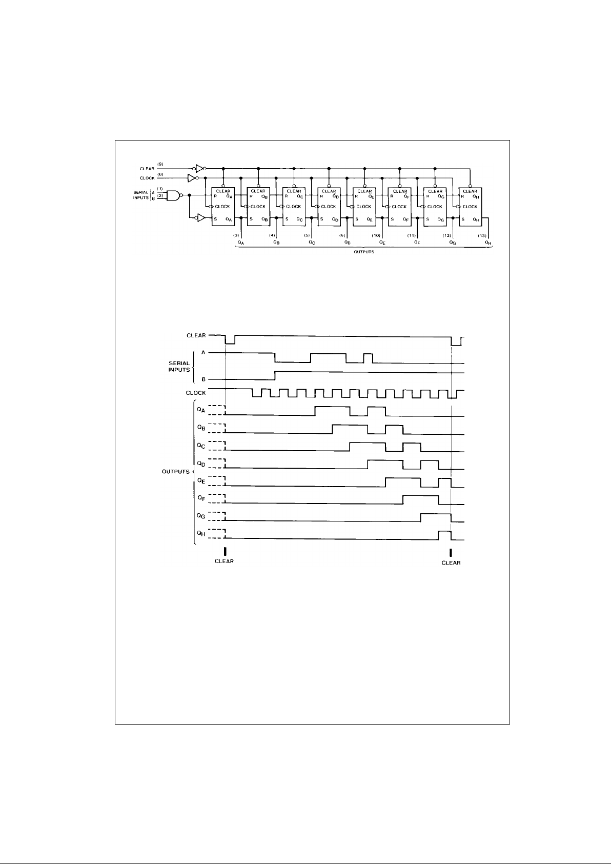
Logic Diagram
Timing Diagram
 Loading...