Fairchild Semiconductor CD4541BCN8, CD4541BCN, CD4541BCMX, CD4541BCM Datasheet

October 1987
Revised March 1999
CD4541BC Programmable Timer
© 1999 Fairchild Semiconductor Corporation DS006001.prf www.fairchildsemi.com
CD4541BC
Programmable Timer
General Description
The CD4541BC Program mable Timer is designed with a
16-stage binary counter, an integrated oscillator for use
with an external capac itor and two resi stors, output control
logic, and a special power-on reset circuit. The special features of the power-on rese t circuit are first, no additional
static power consumpt ion and second, the part functio ns
across the full voltage range (3V–15V ) whether power-on
reset is enabled or disabled.
Timing and the counter are in itialized by tur ning on po wer,
if the power-on reset is enabled. When the power is
already on, an external reset pulse will also initialize the
timing and counter. After either r eset is accomplished , the
oscillator frequency is determined by t he external RC network. The 16-stage counter divides the oscillator frequency
by any of 4 digitally controlled division ratios.
Features
■ Available division ratios 28, 210, 213, or 2
16
■ Increments on positive edge clock transitions
■ Built-in low power RC oscillator (±2% accuracy over
temperature rang e and ±10 % suppl y and ±3% over processing @ < 10 kHz)
■ Oscillator frequency range ≈ DC to 100 kHz
■ Oscillator may be bypassed if external clock is available
(apply external cloc k to pin 3)
■ Automatic reset initializes all counters when power turns
on
■ External master reset t otally independent of automatic
reset operation
■ Operates at 2
n
frequency divider or single transition
timer
■ Q/Q
select provides output logic level flexibility
■ Reset (auto or ma ster) disables oscillator du ring resetting to provide no active power dissipation
■ Clock conditioning circuit permits operation with very
slow clock rise and fall times
■ Wide supply voltage range—3.0V to 15V
■ High noise immunity—0.45 V
DD
(typ.)
■ 5V–10V–15V parameter ratings
■ Symmetrical output characteristics
■ Maximum input leaka ge 1 µA at 15V over full tempera-
ture range
■ High output drive (pin 8) min. one TTL load
Ordering Code:
Devices also availab le in Tape and Reel. Specify by appending th e s uffix let t er “X” to the ordering code.
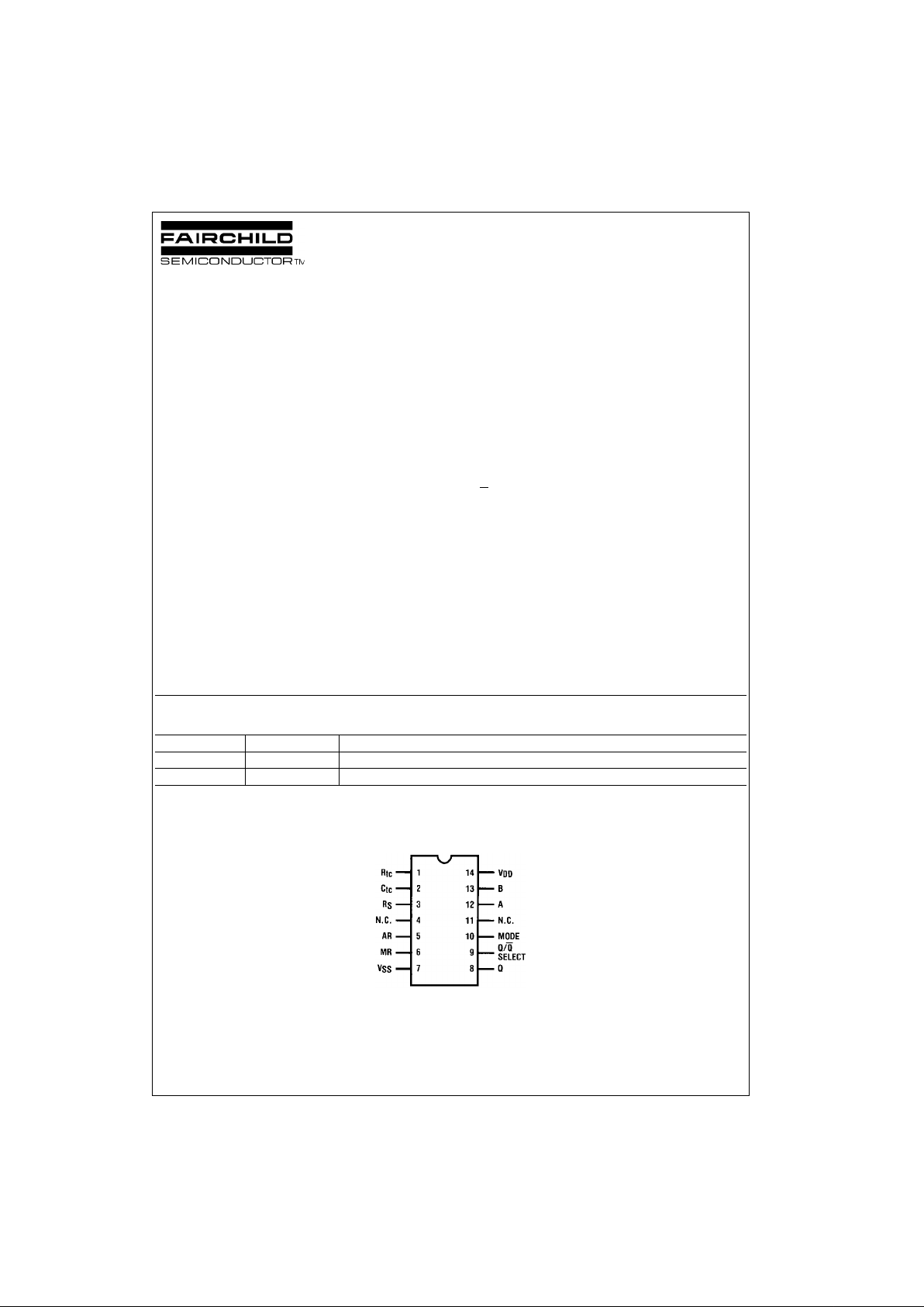
Connection Diagram
Pin Assignments for DIP and SOIC
N.C.—Not connected
Top View
Order Number Package Number Package Description
CD4541BCN N14A 14-Lead Plastic Dual-In-Line Package (PDIP), JEDEC MS-001, 0.300” Wide
CD4541BCM M14A 14-Lead Small Outline Integrated Circuit (SOIC), JEDEC MS-012, 0.150” Narrow

www.fairchildsemi.com 2
CD4541BC
Truth Table Division Ratio Table
Operating Characteristics
With Auto Reset pin set to a “0” the counte r circu it is initialized by turning on power. Or with power already on , the
counter circuit is reset when the Ma ster Re set pin is set to
a “1”. Both types of reset will result in synchronously resetting all counter stages independent of counter state.
The RC oscillator frequency is determined by the external
RC network, i.e.:
and R
S
≈ 2 Rtc where RS ≥ 10 kΩ
The time select inputs (A and B) provide a two-bit address
to output any one of f our counter sta ges (2
8
, 210, 213, and
2
16
). The 2n counts as shown in the Division Ratio Table
represent the Q output of the Nth stage of the counter.
When A is “1”, 2
16
is selected for both states of B.
However, when B is “0”, normal counting is interrupted and
the 9th counter stage receives its clock directly from the
oscillator (i.e., effectively outputting 2
8
).
The Q/Q
select output control pin provides for a choice of
output level. When the counter is in a r eset condition and
Q/Q
select pin is set to a “0” the Q ou tput is a “0”. Corre-
spondingly, when Q/Q
select pin is set to a “1” the Q output
is a “1”.
When the mode control pin is set to a “1”, the selected
count is continually transmitted to the output. But, with
mode pin “0” and after a reset conditi on the RS flip-flop
resets (see Logic Diagram), counting commences and after
2
n−1
counts the RS flip-flop sets which causes the output to
change state. Hence, af ter another 2
n−1
counts the output
will not change. Thus, a Master Reset pulse must be
applied or a chang e in the mode pin lev el is required to
reset the single cycle operation.
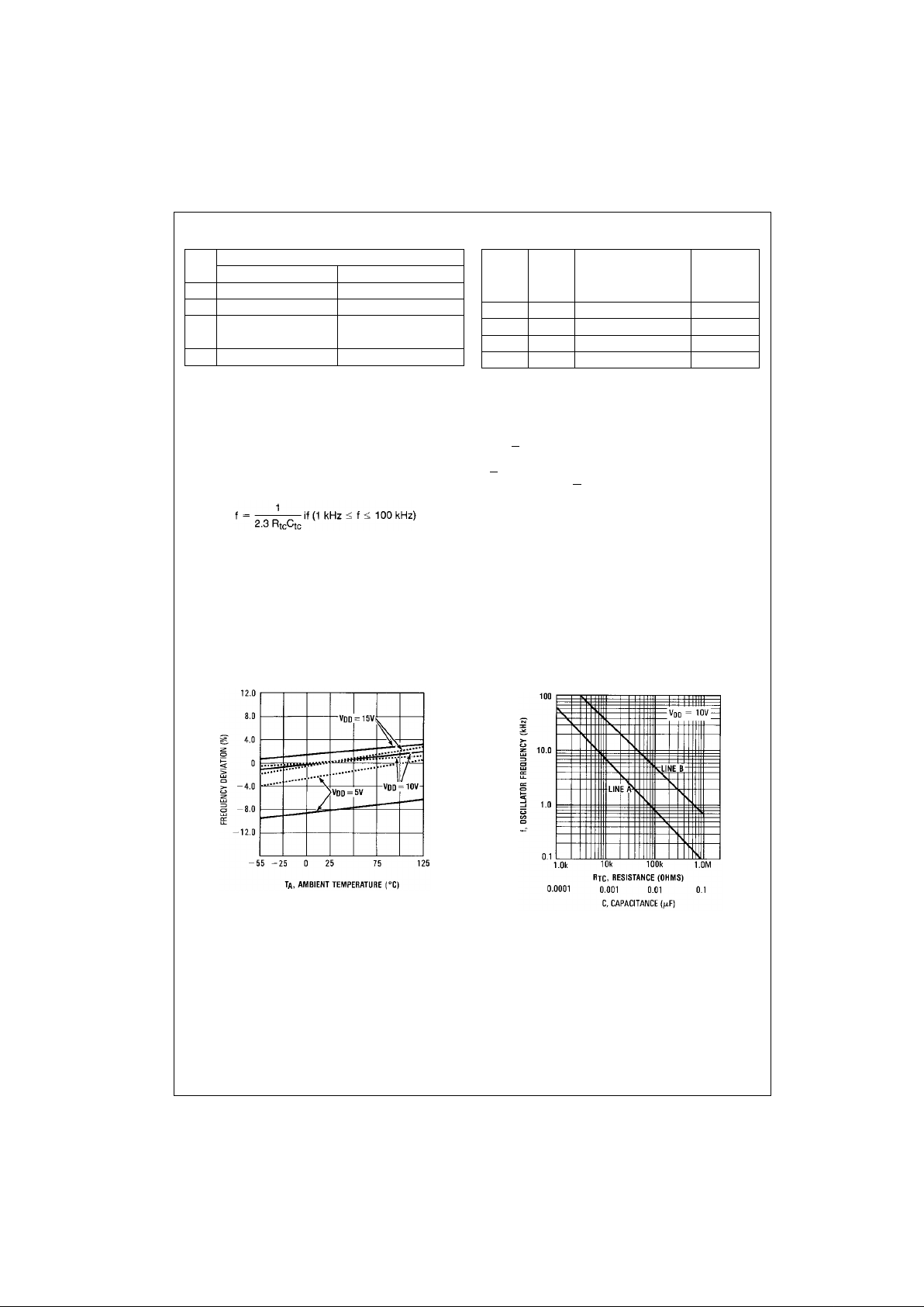
Typical RC Oscillator
Characteristics
Solid Line = RTC = 56 kΩ, RS = 1 kΩ and C = 1000 pF
f = 10.2 kHz @ V
DD
= 10V and TA = 25°
Dashed Line = R
TC
= 56 kΩ, RS = 120 kΩ and C = 1000 pF
f = 7.75 kHz @ V
DD
= 10V and TA = 25°
RC Oscillator Frequency as a
Function of R
TC
and C
Line A: f as a function of C and (RTC = 56 kΩ; RS = 120k
Line B: f as a function of R
TC
and (C = 100 pF; RS = 2 R
TC
Pin State
01
5 Auto Reset Operating Auto Reset Disabled
6 Timer Operational Master Reset On
9 Output Initially Low Output Initially High
after Reset after Reset
10 Single Cycle Mode Re cycle Mod e
Number of Count
A B Counter Stages
2
n
n
0 0 13 8192
0 1 10 1024
10 8 256
1 1 16 65536

3 www.fairchildsemi.com
CD4541BC
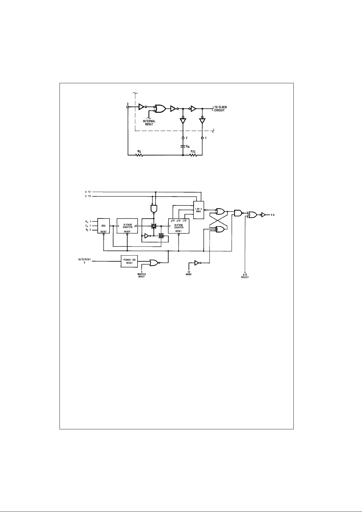
Oscillator Circuit Using RC Configuration
Logic Diagram
VDD = Pin 14
V
SS
= Pin 7
 Loading...