

Fairchild Semiconductor CD4099BCN, CD4099BCCW Datasheet
October 1987
Revised January 1999
CD4099BC 8-Bit Addressable Latch
© 1999 Fairchild Semiconductor Corporation DS005984.prf www.fairchildsemi.com
CD4099BC
8-Bit Addressable Latch
General Description
The CD4099BC is an 8 -bit addressable latch with three
address inputs (A0–A2), an active low enable input (E
),
active high clear input (CL), a data input (D), and eight outputs (Q0–Q7).
Data is en ter e d into a particul ar bi t in th e l a tch w h en th at b i t
is addressed by the address inputs an d the enable (E
) is
LOW. Data entry is inhibited when enable (E
) is HIGH.
When clear (CL) and e nable (E
) are HIGH, all outputs are
LOW. When clear (CL) is HIGH and enable (E
) is LOW, the
channel demultiplexing occurs. Th e bit that is addressed
has an active output which follows the data input while all
unaddressed bits are held LOW. When operating in the
addressable latch mode (E
= CL = LOW), changing more
than one bit of the address cou ld impo se a tra nsi en t wro ng
address. Therefore, this should only be done while in the
memory mode (E
= HIGH, CL = LOW).
Features
■ Wide supply voltage range: 3.0V to 15V
■ High noise immunity: 0.45 V
DD
(typ.)
■ Low power TTL: fan out of 2 driving 74L
compatibility: or 1 driving 74LS
■ Serial to parallel capability
■ Storage register capability
■ Random (addressable) data entry
■ Active high demultiplexing capability
■ Common active high clear
Ordering Code:
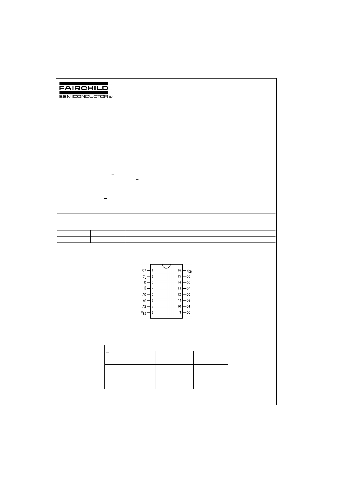
Connection Diagram
Pin Assignments for DIP
Top View
Truth Table
Order Number Package Number Package Description
CD4099BCN N16E 16-Lead Dual-In-Line Package (PDIP), JEDEC MS-001, 0.300” Wide
Mode Selection
E
CL Addressed Unaddressed Mode
Latch Latch
L L Follows Data Holds Previous Data Addressable Latch
H L Holds Previous Data Holds Previous Data Memory
L H Follows Data Reset to “0” Demultiplexer
H H Reset to “0” Reset to “0” Clear
www.fairchildsemi.com 2
CD4099BC
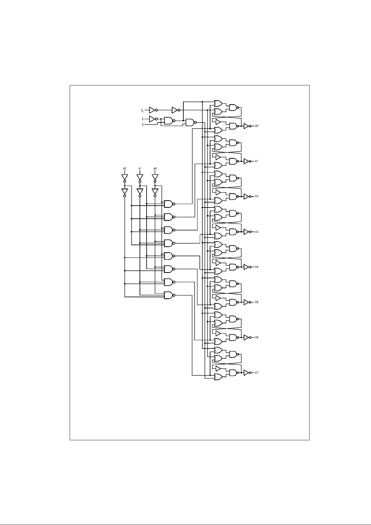
Logic Diagram
 Loading...