

Fairchild Semiconductor BSS64 Datasheet
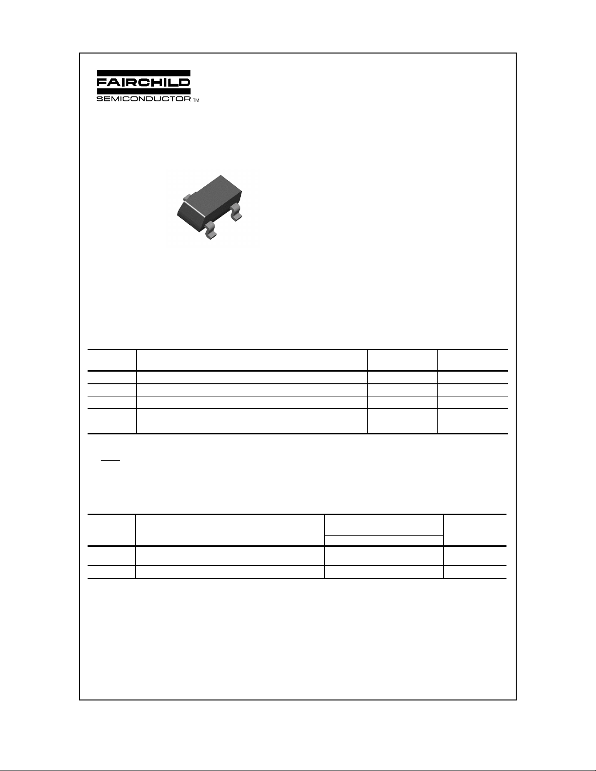
BSS64
C
BSS64
E
SOT-23
Mark: U3
B
NPN General Purpose Amplifier
This device is designed for general purpose high voltage amplifiers
and gas discharge display driving. Sourced from Process 16.
Absolute Maximum Ratings* TA = 25°C unless otherwise noted
Symbol Parameter Value Units
V
CEO
V
CBO
V
EBO
I
C
TJ, T
stg
*These ratings are limiting values above which the serviceability of any semiconductor device may be impaired.
NOTES:
1) These ratings are based on a maximum junction temperature of 150 degrees C.
2) These are steady state limits. The factory should be consulted on applications involving pulsed or low duty cycle operations.
Thermal Characteristics TA = 25°C unless otherwise noted
Collector-Emitter Voltage 80 V
Collector-Base Voltage 120 V
Emitter-Base Voltage 5.0 V
Collector Current - Continuous 200 mA
Operating and Stora ge Junction Temperature Range -55 to +150
°
C
Symbol Characteristic Max Units
*BSS64
P
D
R
θ
JA
Total Devi ce Dissipat ion
Derate above 25°C
Thermal Resistance , Junctio n to Ambient 357
350
2.8
*Device mounted on FR-4 PCB 40 mm X 40 mm X 1.5 mm.
1997 Fairchild Semiconductor Corporation
mW
mW/°C
C/W
°
NPN General Purpose Amplifier
µ
µ
(continued)
Electrical Characteristics TA = 25°C unless otherwise noted
Symbol Parameter Test Conditions Min Max Units
OFF CHARACTERISTICS
V
(BR)CEO
V
(BR)CBO
V
(BR)EBO
I
CBO
I
EBO
ON CHARACTERISTICS
h
FE
V
sat
CE(
V
sat
BE(
SMALL SIGNAL CHARACTERISTICS
f
T
C
ob
Collector-Emitter Breakdown Voltage IC = 4.0 mA, IB = 0 80 V
Collector-Base Breakdown Voltage
Emitter-Base Breakdown Voltage
I
= 100 µA, IE = 0
C
I
= 100 µA, IC = 0
E
120 V
5.0 V
Collector-Cutoff Current VCB = 90 V, IE = 0
V
= 90 V, IE = 0, TA = 150°C
CB
Emitte r-Cutoff Current VEB = 5.0 V, IC = 0 200 nA
DC Current Gain IC = 10 mA, VCE = 1.0 V 20
Collector-Emitter Saturation Voltage
)
Base-Emitter Saturation Voltage
)
Current Gain - Bandwidth Product IC = 4.0 mA, VCE = 10,
= 4.0 mA, IB = 400 µA
I
C
I
= 50 mA, IB = 15 mA
C
I
= 4.0 mA, IB = 400 µA
C
60 MHz
f = 35 MHz
Output Capacitance VCB = 10 V, f = 1.0 MHz 5.0 pF
0.1
50
0.15
0.2
1.2 V
A
A
V
V
BSS64
Spice Model
NPN (Is=2.511f Xti=3 Eg=1.11 V af=100 Bf=242.6 Ne=1.249 Ise=2.51 1f Ikf=.3458 Xtb=1.5 Br=3.197 Nc=2 Isc=0
Ikr=0 Rc=1 Cjc=4.883p Mjc=.3047 Vjc=.75 Fc=.5 Cje=18.79p Mje=.3416 Vje=.75 Tr=1.202n Tf=560p Itf=50m
Vtf=5 Xtf=8 Rb=10)
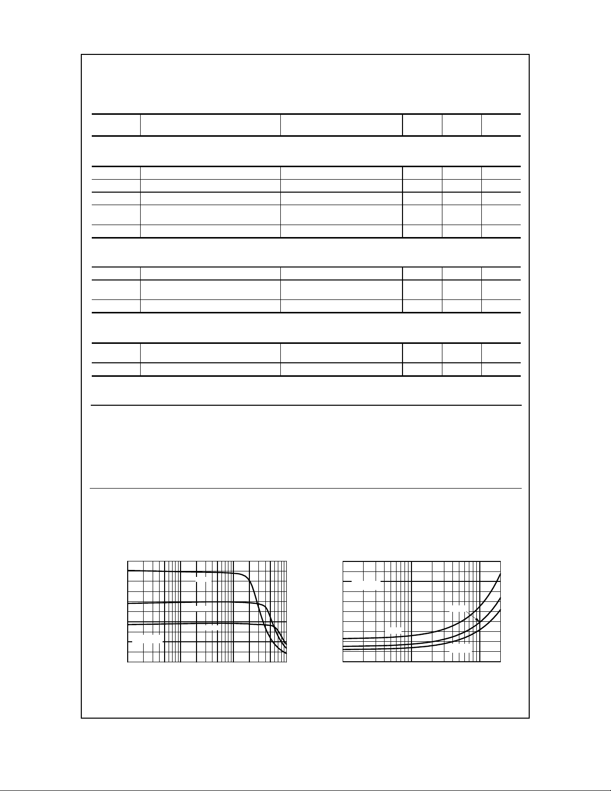
T ypical Characteristics
Typ ical Puls ed Current G ain
vs Collector Current
250
200
150
100
V = 5V
CE
50
0
FE
0.1 0.2 0.5 1 2 5 10 20 50 100
h - TYPICAL PULSED CURRENT GAIN
I - COLLECTOR CURRENT (mA)
C
125 °C
25 °C
- 40 °C
Coll ector -Emitt er Sa turatio n
Voltage vs Co llector Curre nt
0.5
0.4
β
= 10
0.3
0.2
0.1
0
110100200
CE SAT
V - COLLECTOR EMITTER VOLTAGE (V)
125 °C
I - COLLECTOR CURRE NT (mA)
C
25 °C
- 40 °C
3
 Loading...