Fairchild Semiconductor BSS63 Datasheet

BSS63
C
BSS63
E
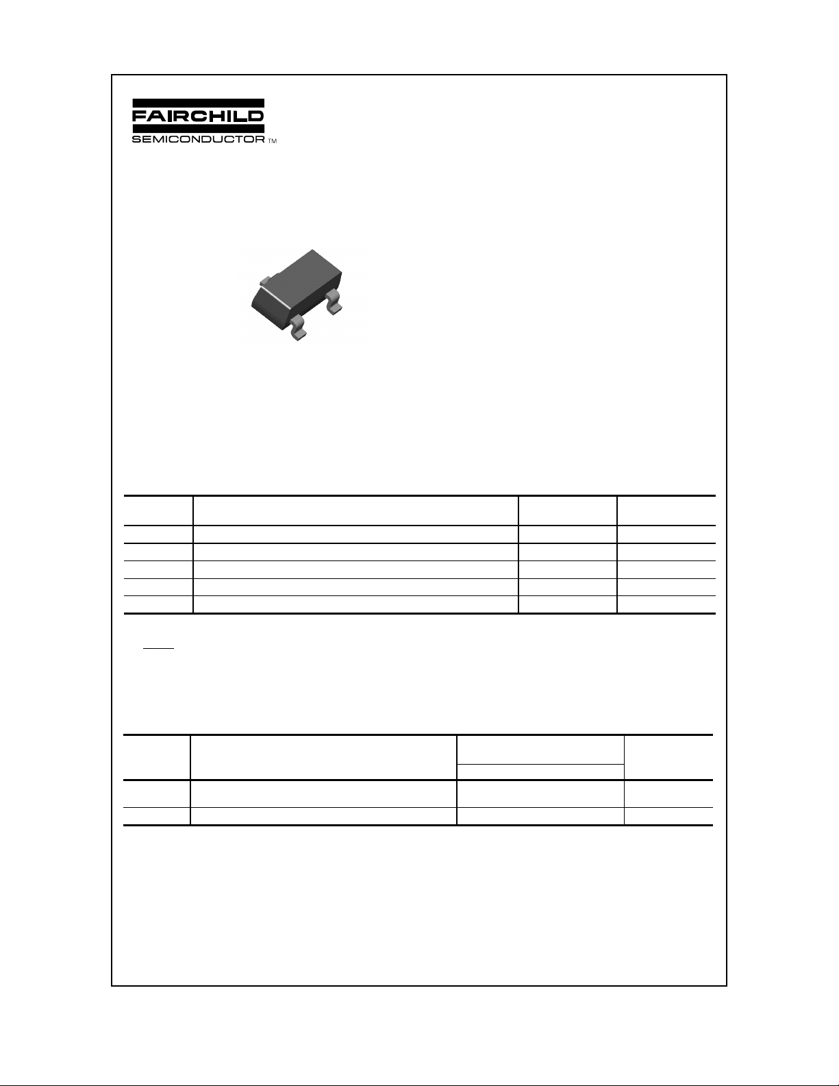
SOT-23
Mark: T3
B
PNP General Purpose Amplifier
This device is designed for general purpose amplifier and switch
applications requiring high voltages. Sourced from Process 74.
Absolute Maximum Ratings* TA = 25°C unless otherwise noted
Symbol Parameter Value Units
V
CEO
V
CBO
V
EBO
I
C
TJ, T
stg
*These ratings are limiting values above which the serviceability of any semiconductor device may be impaired.
NOTES:
1) These ratings are based on a maximum junction temperature of 150 degrees C.
2) These are steady state limits. The factory should be consulted on applications involving pulsed or low duty cycle operations.
3) All voltages (V) and currents (A) are negative polarity for PNP transistors.
Thermal Characteristics TA = 25°C unless otherwise noted
Collector-Emitter Voltage 100 V
Collector-Base Voltage 110 V
Emitter-Base Voltage 6.0 V
Collector Current - Continuous 200 mA
Operating and Stora ge Junction Temperature Range -55 to +150
°
C
3
Symbol Characteristic Max Units
*BSS63
P
D
R
θ
JA
Total Devi ce Dissipat ion
Derate above 25°C
Thermal Resistance , Junctio n to Ambient 357
350
2.8
*Device mounted on FR-4 PCB 40 mm X 40 mm X 1.5 mm.
1997 Fairchild Semiconductor Corporation
mW
mW/°C
C/W
°

µ
PNP General Purpose Amplifier
(continued)
BSS63
Electrical Characteristics
TA = 25°C unless otherwise noted
Symbol Parameter Test Conditions Min Max Units
OFF CHARACTERISTICS
V
(BR)CEO
V
(BR)CBO
V
(BR)EBO
I
CBO
I
EBO
Collector-Emitter Breakdown Voltage
Collector-Base Breakdown Voltage
Emitter-Base Breakdown Voltage
I
= 100 µA, IB = 0
C
= 10 µA, IE = 0
I
C
I
= 1.0 µA, IC = 0
E
Collector-Cutoff Current VCB = 90 V, IE = 0
V
= 90 V, IE = 0, TA = 150°C
CB
100 V
110 V
6.0 V
100
50
nA
Emitte r-Cutoff Current VEB = 6.0 V, IC = 0 200 nA
A
ON CHARACTERISTICS
h
FE
V
sat
CE(
V
sat
BE(
DC Current Gain IC = 10 mA, VCE = 1.0 V
I
= 25 mA, VCE = 1.0 V
Collector-Emitter Saturation Voltage IC = 25 mA, IB =2.5 mA 0.25 V
)
Base-Emitter Saturation Voltage IC = 25 mA, IB =2.5 mA 0.9 V
)
C
30
30
SMALL SIGNAL CHARACTERISTICS
f
T
NOTE: All voltages (V) and currents (A) are negative polarity for PNP transistors.
Current Gain - Bandwidth Product IC = 25 mA, VCE = 5.0,
f = 35 MHz
50 MHz
Spice Model
PNP (Is=21.48f Xti=3 Eg=1.11 Vaf=100 Bf=132.1 Ne=1.375 Ise=21.48f Ikf=.1848 Xtb=1.5 Br=3.661 Nc=2 Isc=0
PNP (Is=21.48f Xti=3 Eg=1.11 Vaf=100 Bf=132.1 Ne=1.375 Ise=21.48f Ikf=.1848 Xtb=1.5 Br=3.661 Nc=2 Isc=0
Ikr=0 Rc=1.6 Cjc=17.63p Mjc=.5312 Vjc=.75 Fc=.5 Cje=73.39p Mje=.3777 Vje=.75 Tr=1.476n Tf=641.9p Itf=0
Ikr=0 Rc=1.6 Cjc=17.63p Mjc=.5312 Vjc=.75 Fc=.5 Cje=73.39p Mje=.3777 Vje=.75 Tr=1.476n Tf=641.9p Itf=0
Vtf=0 Xtf=0 Rb=10)
Vtf=0 Xtf=0 Rb=10)
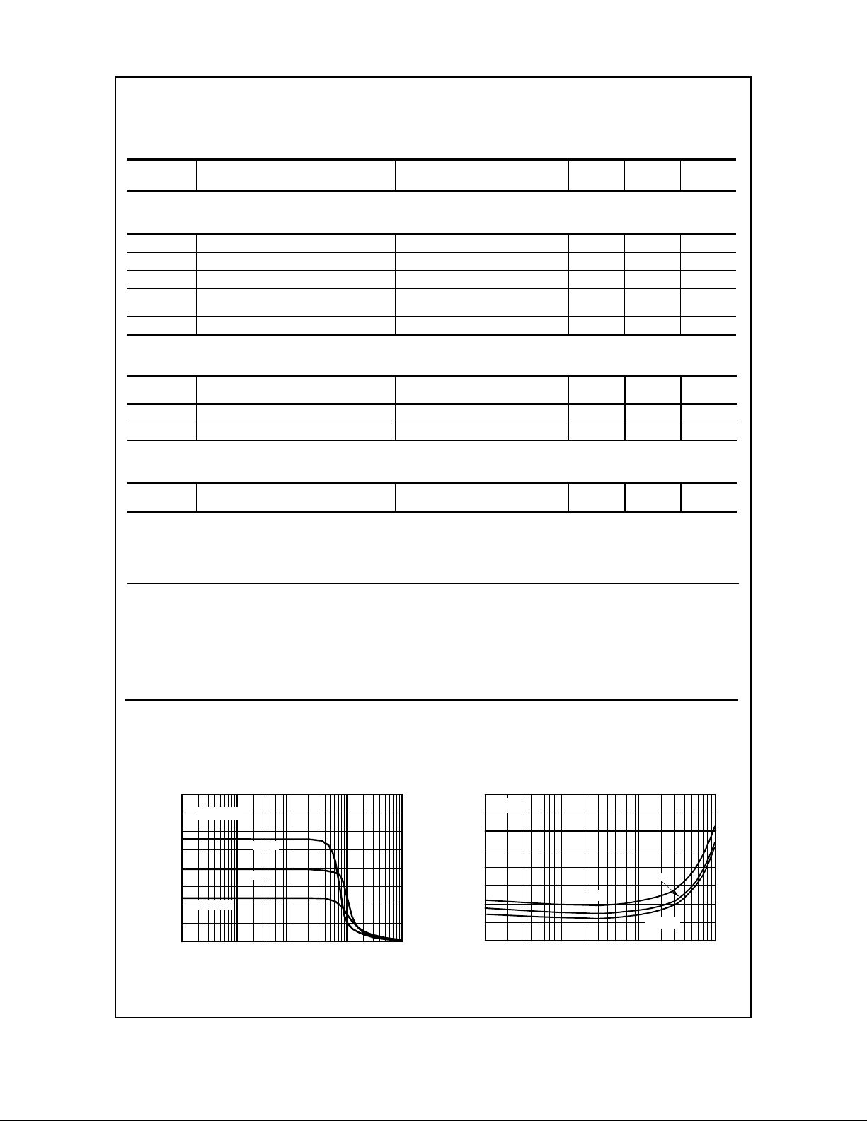
T ypical Characteristics
Typical Puls ed Current Gain
vs Collector Current
200
V = 5V
CE
150
100
- 40 °C
50
0
FE
0.0001 0.001 0.01 0.1 1
h - TYPICAL PULSED CUR RENT GAI N
125 °C
25 °C
I - COL L ECTOR CURRE NT (A)
C
Collecto r- Emi tter Saturation
V o lt age vs C o llec tor Cur rent
0.4
= 10
β
0.3
0.2
0.1
0
0.1 1 10 100
CESAT
V - COLLECTOR-EMITTER VOLTAGE (V)
I - COLLECTOR CURRENT (mA)
C
125 °C
25 °C
- 40 °C
 Loading...