

October 2013
FAN54015 — USB-Compliant Single-Cell Li-Ion Switching Charger with USB-OTG Boost Regulator
FAN54015
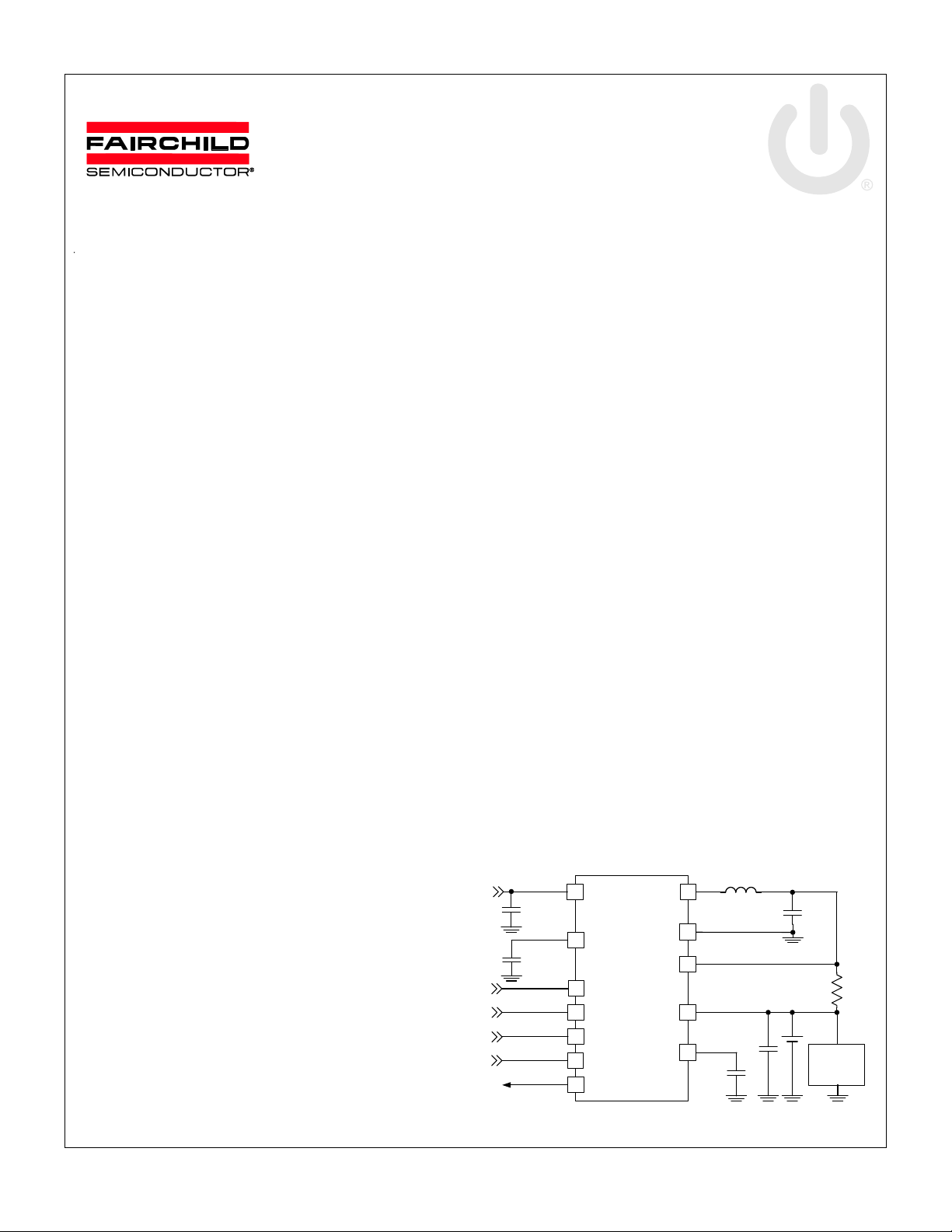
SW
PGND
C
OUT
L1
VBAT
+
Battery
CSIN
R
SENSE
68m
1H
C
BAT
SYSTEM
LOAD
0.1F
1F
4.7F
SDA
SCL
OTG/USB#
C
REG
1F
VREG
STAT
10F
DISABLE
C
BUS
C
MID
VBUS
PMID
All trademarks are the property of their respective owners.
FAN54015
USB-Compliant Single-Cell Li-Ion Switching Charger with
USB-OTG Boost Regulator
Features
Fully Integrated, High-Efficiency Charger for Single-Cell
Li-Ion and Li-Polymer Battery Packs
Faster Charging than Linear
Charge Voltage Accuracy: 0.5% at 25°C
1% from 0 to 125°C
5% Input Current Regulation Accuracy
5% Charge Current Regulation Accuracy
20 V Absolute Maximum Input Voltage
6 V Maximum Input Operating Voltage
1.45 A Maximum Charge Rate
Programmable through High-Speed I
(3.4 Mb/s) with Fast Mode Plus Compatibility
2
C Interface
– Input Current
– Fast-Charge / Termination Current
– Charger Voltage
– Termination Enable
3 MHz Synchronous Buck PWM Controller with Wide
Duty Cycle Range
Small Footprint 1 H External Inductor
Safety Timer with Reset Control
1.8 V Regulated Output from VBUS for Auxiliary Circuits
Dynamic Input Voltage Control
Low Reverse Leakage to Prevent Battery Drain to VBUS
5 V, 500 mA Boost Mode for USB OTG for 3.0 V to
4.5 V Battery Input
Available in a 1.96 x 1.87 mm, 20-bump, 0.4 mm Pitch
WLCSP Package
Description
The FAN54015 combines a highly integrated switch-mode
charger, to minimize single-cell Lithium-ion (Li-ion) charging
time from a USB power source, and a boost regulator to
power a USB peripheral from the battery.
The charging parameters and operating modes are
programmable through an I2C Interface that operates up to
3.4 Mbps. The charger and boost regulator circuits switch at
3 MHz to minimize the size of external passive components.
The FAN54015 provides battery charging in three phases:
conditioning, constant current and constant voltage.
To ensure USB compliance and minimize charging time, the
input current limit can be changed through the I2C by the
host processor. Charge termination is determined by a
programmable minimum current level. A safety timer with
reset control provides a safety backup for the I2C host.
Charge status is reported to the host through the I2C port.
The integrated circuit (IC) automatically restarts the charge
cycle when the battery falls below an internal threshold. If the
input source is removed, the IC enters a high-impedance
mode, preventing leakage from the battery to the input.
Charge current is reduced when the die temperature reaches
120°C, protecting the device and PCB from damage.
The FAN54015 can operate as a boost regulator on
command from the system. The boost regulator includes a
soft-start that limits inrush current from the battery and uses
the same external components used for charging the battery.
Applications
Cell Phones, Smart Phones, PDAs
Tablet, Portable Media Players
Gaming Device, Digital Cameras
© 2012 Fairchild Semiconductor Corporation www.fairchildsemi.com
FAN54015 • Rev. 1.0.2
Figure 1. Typical Application
FAN54015 — USB-Compliant Single-Cell Li-Ion Switching Charger with USB-OTG Boost Regulator
Part Number
Temperature
Range
Package
PN Bits:
IC_INFO[4:2]
Packing
Method
FAN54015UCX
-40 to 85°C
20-Bump, Wafer-Level Chip-Scale Package (WLCSP),
0.4 mm Pitch, Estimated Size: 1.96 x 1.87 mm
101
Tape and
Reel
FAN54015BUCX
(1)
Part Number
Slave Address
Automatic
Charge
Special
Charger
(2)
Safety
Limits
Battery Absent
Behavior
E2 Pin
VREG
(E3 Pin)
FAN54015UCX
1101010
Yes
Yes
Yes
ON
DISABLE
1.8 V
PWM
MODULATOR
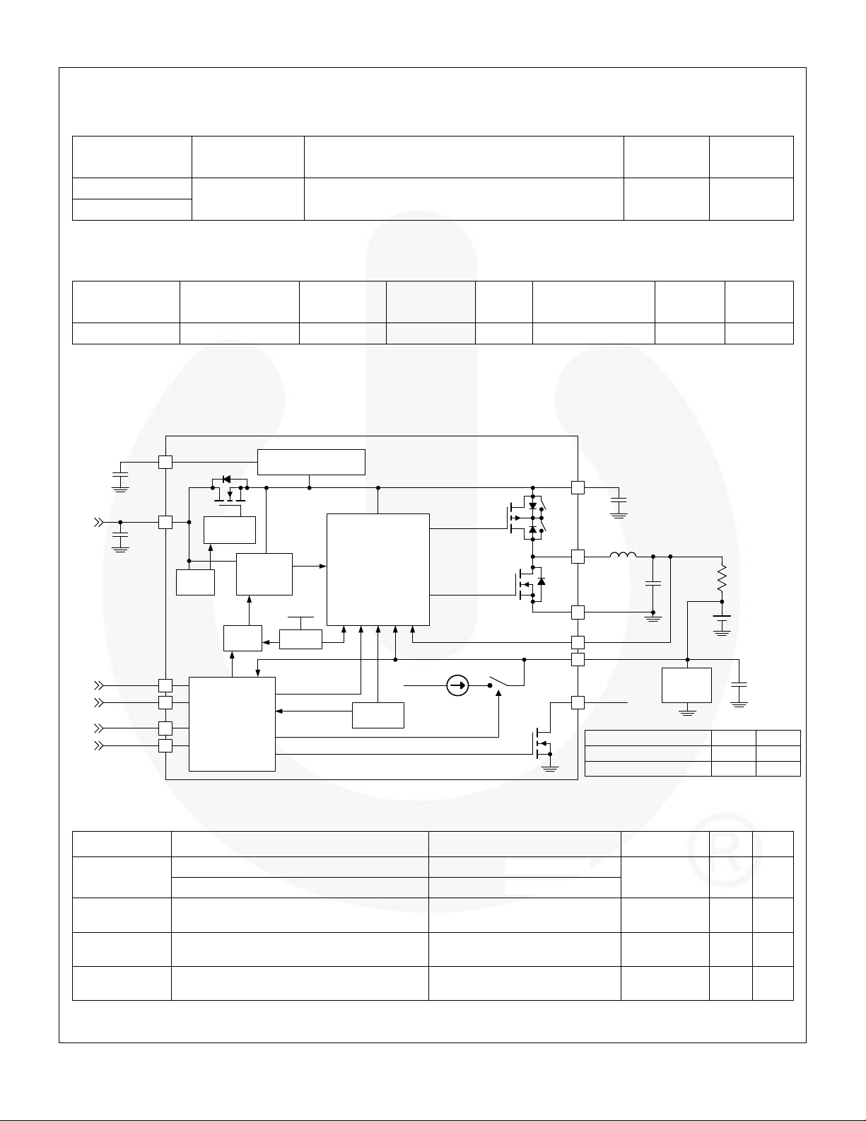
PMID
SW
PGND
PMID
L1
VBAT
C
MID
+
Battery
CSIN
1H
4.7F
C
BAT
SYSTEM
LOAD
VREF
SDA
SCL
OTG/USB#
VCC
VBUS
C
BUS
1F
STAT
I2C
INTERFACE
LOGIC
AND
CONTROL
PMID
OSC
30mA
C
OUT
0.1F
R
SENSE
Q3
CHARGE
PUMP
VBUS
OVP
I_IN
CONTROL
VREG
C
REG
1F
DAC
DISABLE
1.8V / PMID REG
Q2
Q1B
Q1A
Q1
Component
Description
Vendor
Parameter
Typ.
Unit
L1
1 H ±20%, 1.6 A, DCR=55 m, 2520
Murata: LQM2HPN1R0
L
1.0
H
1 H ±30%, 1.4 A, DCR=85 m, 2016
Murata: LQM2MPN1R0
C
BAT
10 F, 20%, 6.3 V, X5R, 0603
Murata: GRM188R60J106M
TDK: C1608X5R0J106M
C
10
F
C
MID
4.7 F, 10%, 6.3 V, X5R, 0603
Murata: GRM188R60J475K
TDK: C1608X5R0J475K
C
(3)
4.7
F
C
BUS
1.0 F, 10%, 25 V, X5R, 0603
Murata GRM188R61E105K
TDK:C1608X5R1E105M
C
1.0
F
PMID
Q1A
Q1B
Greater than V
BAT
ON
OFF
Less than V
BAT
OFF
ON
Ordering Information
Note:
1. FAN54015BUCX includes backside lamination.
Table 1. Feature Summary
Note:
2. A “special charger” is a current-limited charger that is not a USB compliant source.
Block Diagram
Table 2. Recommended External Components
© 2012 Fairchild Semiconductor Corporation www.fairchildsemi.com
FAN54015 • Rev. 1.0.2 2
Note:
3. A 6.3 V rating is sufficient for C
because PMID is protected from over-voltage surges on VBUS by Q3 (Figure 2).
MID
Figure 2. IC and System Block Diagram
FAN54015 — USB-Compliant Single-Cell Li-Ion Switching Charger with USB-OTG Boost Regulator
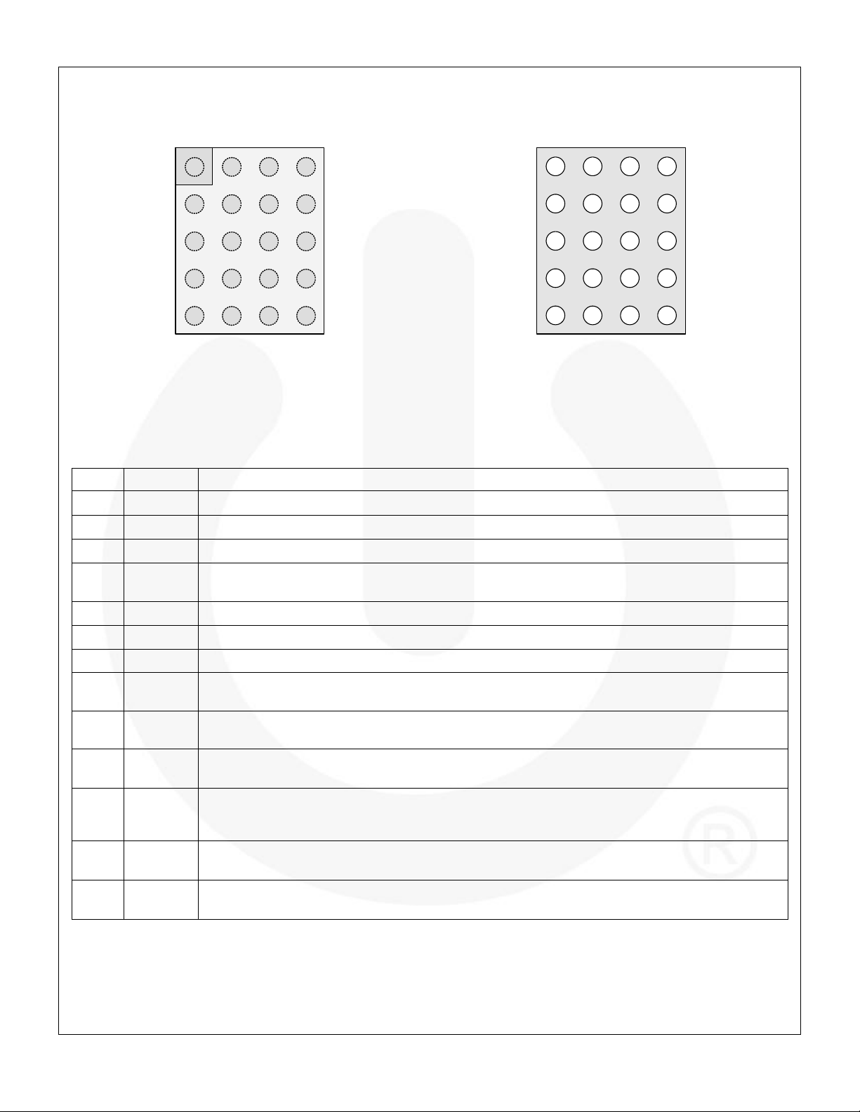
Top View
Bottom View
Figure 3. WLCSP-20 Pin Assignments
Pin #
Name
Description
A1, A2
VBUS
Charger Input Voltage and USB-OTG output voltage. Bypass with a 1 F capacitor to PGND.
A3
NC
No Connect. No external connection is made between this pin and the IC’s internal circuitry.
A4
SCL
I2C Interface Serial Clock. This pin should not be left floating.
B1-B3
PMID
Power Input Voltage. Power input to the charger regulator, bypass point for the input current sense,
and high-voltage input switch. Bypass with a minimum of 4.7 F, 6.3 V capacitor to PGND.
B4
SDA
I2C Interface Serial Data. This pin should not be left floating.
C1-C3
SW
Switching Node. Connect to output inductor.
C4
STAT
Status. Open-drain output indicating charge status. The IC pulls this pin LOW when charging.
D1-D3
PGND
Power Ground. Power return for gate drive and power transistors. The connection from this pin to the
bottom of C
MID
should be as short as possible.
D4
OTG
On-The-Go. Enables boost regulator in conjunction with OTG_EN and OTG_PL bits (see Table 16). On
VBUS Power-On Reset (POR), this pin sets the input current limit for t
15MIN
charging.
E1
CSIN
Current-Sense Input. Connect to the sense resistor in series with the battery. The IC uses this node to
sense current into the battery. Bypass this pin with a 0.1 F capacitor to PGND.
E2
DISABLE
Charge Disable. If this pin is HIGH, charging is disabled. When LOW, charging is controlled by the
I2C registers. When this pin is HIGH, the 15-minute timer is reset. This pin does not affect the
32-second timer.
E3
VREG
Regulator Output. Connect to a 1 F capacitor to PGND. This pin can supply up to 2mA of DC load
current. The output voltage is PMID, which is limited to 1.8 V.
E4
VBAT
Battery Voltage. Connect to the positive (+) terminal of the battery pack. Bypass with a 0.1 F
capacitor to PGND if the battery is connected through long leads.
C1
B1
A1 A2
C3
B3
A3
C2
D1 D3D2
B2
C4
B4
A4
D4
E1 E3E2 E4
C1
B1
A1
C3
B3
A3 A2
C2
D1D3 D2
B2
C4
B4
A4
D4
E1E3 E2E4
Pin Configuration
Pin Definitions
© 2012 Fairchild Semiconductor Corporation www.fairchildsemi.com
FAN54015 • Rev. 1.0.2 3
FAN54015 — USB-Compliant Single-Cell Li-Ion Switching Charger with USB-OTG Boost Regulator
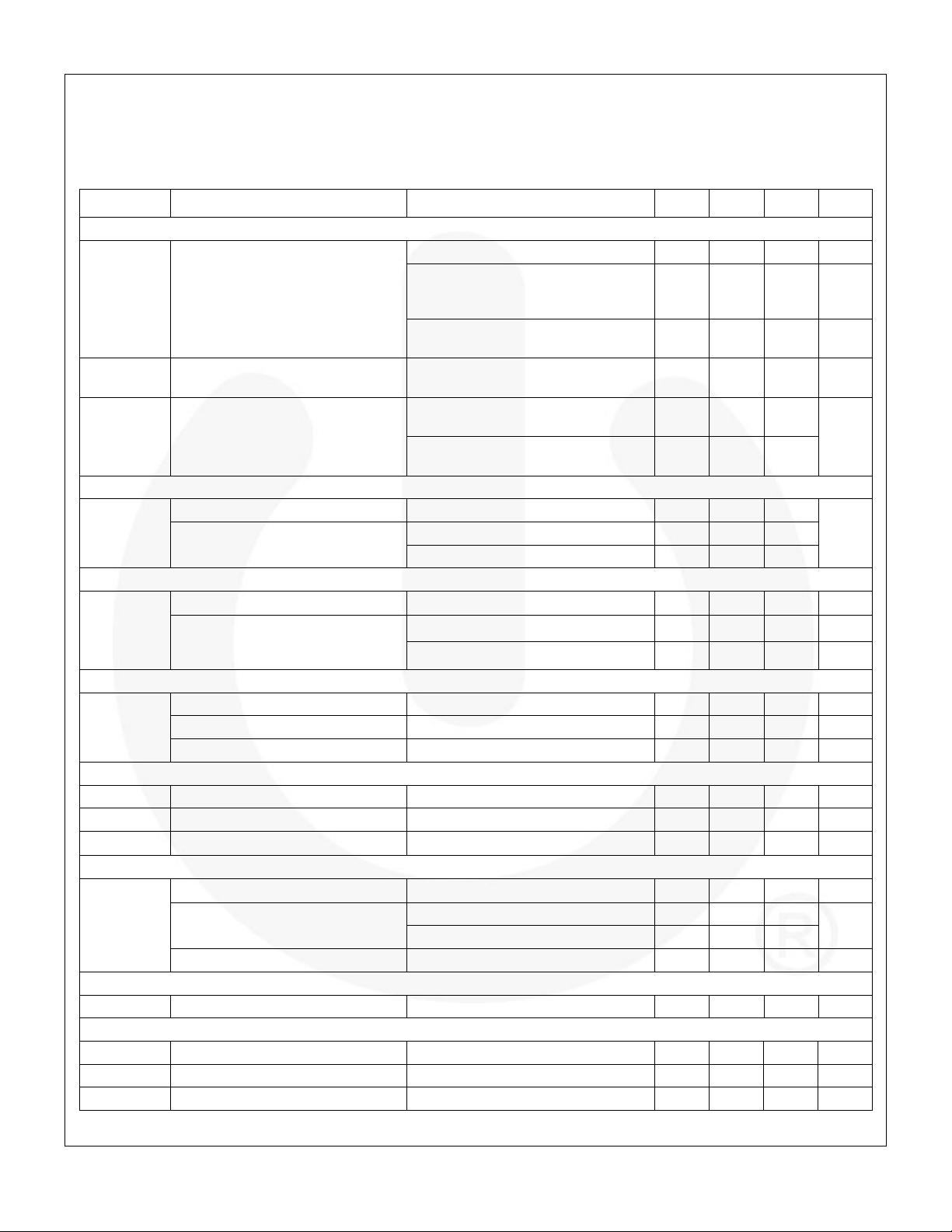
Symbol
Parameter
Min.
Max.
Unit
V
BUS
VBUS Voltage
Continuous
–1.4
20.0
V
Pulsed, 100 ms Maximum Non-Repetitive
–2.0
V
STAT
STAT Voltage
–0.3
16.0
V
VI
PMID Voltage
7.0
V
SW, CSIN, VBAT, DISABLE Voltage
–0.3
7.0
VO
Voltage on Other Pins
–0.3
6.5
(4)
V
dt
dV
BUS
Maximum V
BUS
Slope above 5.5 V when Boost or Charger are Active
4
V/s
ESD
Electrostatic Discharge
Protection Level
Human Body Model per JESD22-A114
2000
V
Charged Device Model per JESD22-C101
500
TJ
Junction Temperature
–40
+150
°C
T
STG
Storage Temperature
–65
+150
°C
TL
Lead Soldering Temperature, 10 Seconds
+260
°C
Symbol
Parameter
Min.
Max.
Unit
V
BUS
Supply Voltage
4 6 V
V
BAT(MAX)
Maximum Battery Voltage when Boost enabled
4.5
V
dt
dV
BUS
Negative VBUS Slew Rate during VBUS Short Circuit,
C
MID
< 4.7 F (see VBUS Short While Charging)
TA < 60°C
4
V/s
TA > 60°C
2 TA
Ambient Temperature
–30
+85
°C
TJ
Junction Temperature (see Thermal Regulation and Protection section)
–30
+120
°C
Symbol
Parameter
Typical
Unit
JA
Junction-to-Ambient Thermal Resistance
60
°C/W
JB
Junction-to-PCB Thermal Resistance
20
°C/W
Absolute Maximum Ratings
Stresses exceeding the absolute maximum ratings may damage the device. The device may not function or be operable above
the recommended operating conditions and stressing the parts to these levels is not recommended. In addition, extended
exposure to stresses above the recommended operating conditions may affect device reliability. The absolute maximum
ratings are stress ratings only.
Note:
4. Lesser of 6.5 V or VI + 0.3 V.
Recommended Operating Conditions
The Recommended Operating Conditions table defines the conditions for actual device operation. Recommended operating
conditions are specified to ensure optimal performance to the datasheet specifications. Fairchild does not recommend
exceeding them or designing to absolute maximum ratings.
Thermal Properties
Junction-to-ambient thermal resistance is a function of application and board layout. This data is measured with four-layer
2s2p boards in accordance to JEDEC standard JESD51. Special attention must be paid not to exceed junction temperature
T
at a given ambient temperature TA. For measured data, see Table 11.
J(max)
© 2012 Fairchild Semiconductor Corporation www.fairchildsemi.com
FAN54015 • Rev. 1.0.2 4
FAN54015 — USB-Compliant Single-Cell Li-Ion Switching Charger with USB-OTG Boost Regulator
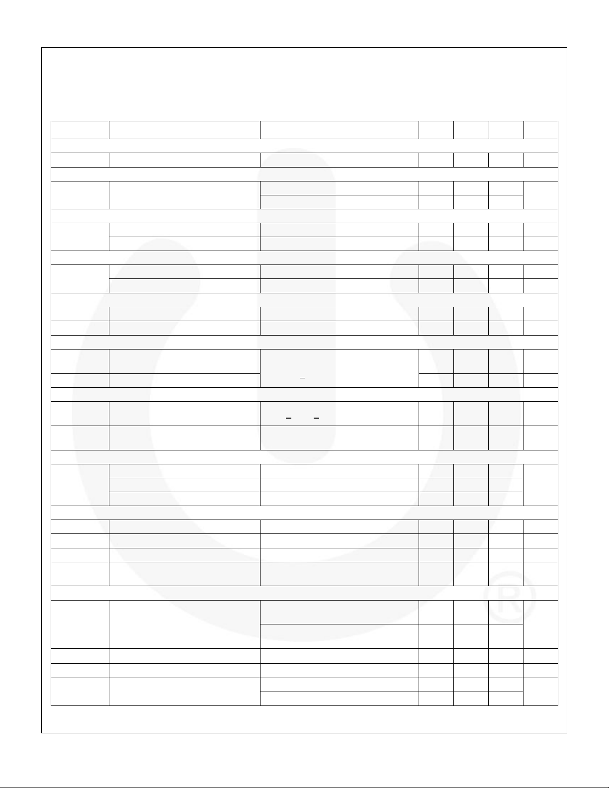
Electrical Specifications
Unless otherwise specified: according to the circuit of Figure 1; recommended operating temperature range for TJ and TA;
V
BUS
=5.0 V; HZ_MODE; OPA_MODE=0; (Charge Mode); SCL, SDA, OTG=0 or 1.8 V; and typical values are for TJ=25°C.
Symbol
Parameter
Conditions
Min.
Typ.
Max.
Unit
Power Supplies
I
VBUS
VBUS Current
V
BUS
> V
BUS(min)
, PWM Switching
10 mA
V
BUS
> V
BUS(min)
; PWM Enabled,
Not Switching (Battery OVP
Condition); I_IN Setting=100 mA
2.5 mA
0°C < TJ < 85°C, HZ_MODE=1
V
BAT
< V
LOWV
, 32S Mode
63
90
A
I
LKG
VBAT to VBUS Leakage Current
0°C < TJ < 85°C, HZ_MODE=1,
V
BAT
=4.2 V, V
BUS
=0 V
0.2
5.0
A
I
BAT
Battery Discharge Current in HighImpedance Mode
0°C < TJ < 85°C, HZ_MODE=1,
V
BAT
=4.2 V
20
A
DISABLE=1, 0°C < TJ < 85°C,
V
BAT
=4.2 V
10
Charger Voltage Regulation
V
OREG
Charge Voltage Range
3.5 4.4
V
Charge Voltage Accuracy
TA=25°C
–0.5%
+0.5%
TJ=0 to 125°C
–1%
+1%
Charging Current Regulation
I
OCHRG
Output Charge Current Range
V
LOWV
< V
BAT
< V
OREG
, R
SENSE
=68 m
550
1450
mA
Charge Current Accuracy Across
R
SENSE
20 mV ≤ V
IREG
≤ 40 mV
92
97
102
%
V
IREG
> 40 mV
94
97
100
%
Weak Battery Detection
V
LOWV
Weak Battery Threshold Range
3.4 3.7
V
Weak Battery Threshold Accuracy
–5 +5
%
Weak Battery Deglitch Time
Rising Voltage
30 ms
Logic Levels: DISABLE, SDA, SCL, OTG
VIH
High-Level Input Voltage
1.05 V VIL
Low-Level Input Voltage
0.4
V
IIN
Input Bias Current
Input Tied to GND or VIN
0.01
1.00
A
Charge Termination Detection
I
(TERM)
Termination Current Range
V
BAT
> V
OREG
– V
RCH
, R
SENSE
=68 m
50 400
mA
Termination Current Accuracy
[V
CSIN
– V
BAT
] from 3 mV to 20 mV
–25 +25
%
[V
CSIN
– V
BAT
] from 20 mV to 40 mV
–5 +5
Termination Current Deglitch Time
2 mV Overdrive
30 ms
1.8V Linear Regulator
V
REG
1.8V Regulator Output
I
REG
from 0 to 2 mA
1.7
1.8
1.9
V
Input Power Source Detection
V
IN(MIN)1
VBUS Input Voltage Rising
To Initiate and Pass VBUS Validation
4.29
4.42
V
V
IN(MIN)2
Minimum VBUS During Charge
During Charging
3.71
3.94
V
t
VBUS_VALID
VBUS Validation Time
30 ms
Continued on the following page…
© 2012 Fairchild Semiconductor Corporation www.fairchildsemi.com
FAN54015 • Rev. 1.0.2 5
FAN54015 — USB-Compliant Single-Cell Li-Ion Switching Charger with USB-OTG Boost Regulator
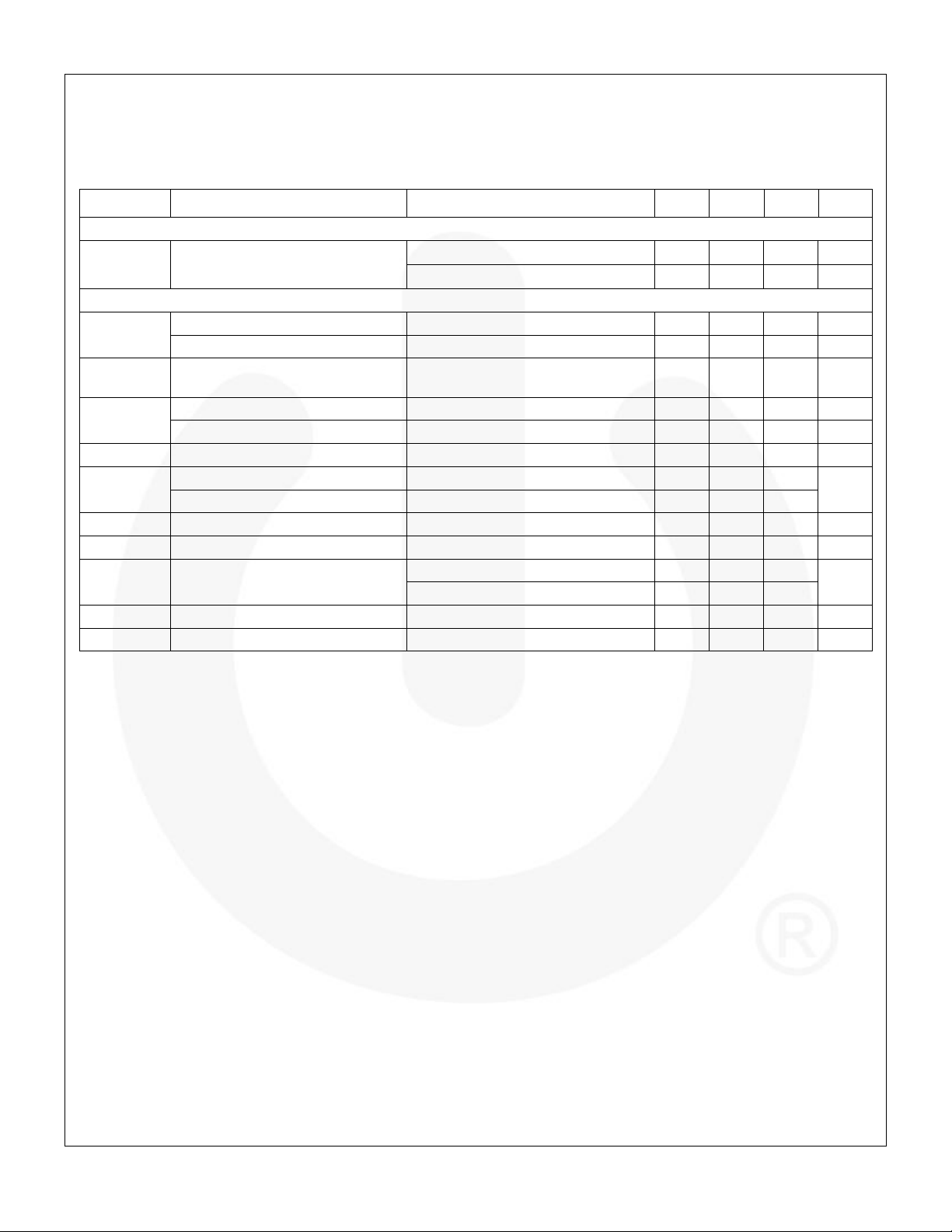
Electrical Specifications
Unless otherwise specified: according to the circuit of Figure 1; recommended operating temperature range for TJ and TA;
V
BUS
=5.0 V; HZ_MODE; OPA_MODE=0; (Charge Mode); SCL, SDA, OTG=0 or 1.8 V; and typical values are for TJ=25°C.
Symbol
Parameter
Conditions
Min.
Typ.
Max.
Unit
Special Charger (V
BUS
)
VSP
Special Charger Setpoint Accuracy
–3 +3
%
Input Current Limit
I
INLIM
Input Current Limit Threshold
IIN Set to 100 mA
88
93
98
mA
IIN Set to 500 mA
450
475
500
V
REF
Bias Generator
V
REF
Bias Regulator Voltage
V
BUS
> V
IN(MIN)
or V
BAT
> V
BAT(MIN)
6.5
V
Short-Circuit Current Limit
20 mA
Battery Recharge Threshold
V
RCH
Recharge Threshold
Below V
(OREG)
100
120
150
mV
Deglitch Time
V
BAT
Falling Below V
RCH
Threshold
130 ms
STAT Output
V
STAT(OL)
STAT Output Low
I
STAT
=10 mA
0.4
V
I
STAT(OH)
STAT High Leakage Current
V
STAT
=5 V
1
A
Battery Detection
I
DETECT
Battery Detection Current before
Charge Done (Sink Current)
(5)
Begins after Termination Detected
and V
BAT
< V
OREG
–V
RCH
–0.80 mA
t
DETECT
Battery Detection Time
262 ms
Sleep Comparator
V
SLP
Sleep-Mode Entry Threshold,
V
BUS
– V
BAT
2.3 V < V
BAT
< V
OREG
, V
BUS
Falling
0
0.04
0.10 V t
SLP_EXIT
Deglitch Time for VBUS Rising
Above V
BAT
by V
SLP
Rising Voltage
30 ms
Power Switches (see Figure 2)
R
DS(ON)
Q3 On Resistance (VBUS to PMID)
I
IN(LIMIT)
=500 mA
180
250
mΩ
Q1 On Resistance (PMID to SW)
130
225
Q2 On Resistance (SW to GND)
150
225
Charger PWM Modulator
fSW
Oscillator Frequency
2.7
3.0
3.3
MHz
D
MAX
Maximum Duty Cycle
100
%
D
MIN
Minimum Duty Cycle
0 %
I
SYNC
Synchronous to Non-Synchronous
Current Cut-Off Threshold
(6)
Low-Side MOSFET (Q2) Cycle-byCycle Current Limit
140 mA
Boost Mode Operation (OPA_MODE=1, HZ_MODE=0)
V
BOOST
Boost Output Voltage at VBUS
2.5 V < V
BAT
< 4.5 V, I
LOAD
from 0 to
200 mA
4.80
5.07
5.17
V
3.0 V < V
BAT
< 4.5 V, I
LOAD
from 0 to
500 mA
4.77
5.07
5.17
I
BAT(BOOST)
Boost Mode Quiescent Current
PFM Mode, V
BAT
=3.6 V, I
OUT
=0
140
300
A
I
LIMPK(BST)
Q2 Peak Current Limit
1272
1590
1908
mA
UVLO
BST
Minimum Battery Voltage for Boost
Operation
While Boost Active
2.42
V
To Start Boost Regulator
2.58
2.70
Continued on the following page…
© 2012 Fairchild Semiconductor Corporation www.fairchildsemi.com
FAN54015 • Rev. 1.0.2 6
FAN54015 — USB-Compliant Single-Cell Li-Ion Switching Charger with USB-OTG Boost Regulator
Electrical Specifications
Unless otherwise specified: according to the circuit of Figure 1; recommended operating temperature range for TJ and TA;
V
BUS
=5.0 V; HZ_MODE; OPA_MODE=0; (Charge Mode); SCL, SDA, OTG=0 or 1.8 V; and typical values are for TJ=25°C.
Symbol
Parameter
Conditions
Min.
Typ.
Max.
Unit
VBUS Load Resistance
R
VBUS
VBUS to PGND Resistance
Normal Operation
1500
k
Charger Validation
100
Protection and Timers
VBUS
OVP
VBUS Over-Voltage Shutdown
V
BUS
Rising
6.09
6.29
6.49
V
Hysteresis
V
BUS
Falling
100 mV
I
LIMPK(CHG)
Q1 Cycle-by-Cycle Peak Current
Limit
Charge Mode
2.3
A
V
SHORT
Battery Short-Circuit Threshold
V
BAT
Rising
1.95
2.00
2.05
V
Hysteresis
V
BAT
Falling
100 mV
I
SHORT
Linear Charging Current
V
BAT
< V
SHORT
20
30
40
mA
T
SHUTDWN
Thermal Shutdown Threshold
(7)
TJ Rising
145
°C
Hysteresis
(7)
TJ Falling
10
TCF
Thermal Regulation Threshold
(7)
Charge Current Reduction Begins
120 °C
t
INT
Detection Interval
2.1 s
t
32S
32-Second Timer
(8)
Charger Enabled
20.5
25.2
28.0
s
Charger Disabled
18.0
25.2
34.0
t
15MIN
15-Minute Timer
15-Minute Mode
12.0
13.5
15.0
min
∆tLF
Low-Frequency Timer Accuracy
Charger Inactive
–25 25
%
Notes:
5. Negative current is current flowing from the battery to VBUS (discharging the battery).
6. Q2 always turns on for 60 ns, then turns off if current is below I
SYNC
.
7. Guaranteed by design; not tested in production.
8. This tolerance (%) applies to all timers on the IC, including soft-start and deglitching timers.
© 2012 Fairchild Semiconductor Corporation www.fairchildsemi.com
FAN54015 • Rev. 1.0.2 7
FAN54015 — USB-Compliant Single-Cell Li-Ion Switching Charger with USB-OTG Boost Regulator
I2C Timing Specifications
Guaranteed by design.
Symbol
Parameter
Conditions
Min.
Typ.
Max.
Unit
f
SCL
SCL Clock Frequency
Standard Mode
100
kHz
Fast Mode
400
High-Speed Mode, CB < 100 pF
3400
High-Speed Mode, CB < 400 pF
1700
t
BUF
Bus-Free Time between STOP
and START Conditions
Standard Mode
4.7
s
Fast Mode
1.3
t
HD;STA
START or Repeated START
Hold Time
Standard Mode
4
s
Fast Mode
600 ns
High-Speed Mode
160 ns
t
LOW
SCL LOW Period
Standard Mode
4.7
s
Fast Mode
1.3
s
High-Speed Mode, CB < 100 pF
160 ns
High-Speed Mode, CB < 400 pF
320 ns
t
HIGH
SCL HIGH Period
Standard Mode
4
s
Fast Mode
600 ns
High-Speed Mode, CB < 100 pF
60 ns
High-Speed Mode, CB < 400 pF
120 ns
t
SU;STA
Repeated START Setup Time
Standard Mode
4.7
s
Fast Mode
600 ns
High-Speed Mode
160 ns
t
SU;DAT
Data Setup Time
Standard Mode
250
ns
Fast Mode
100
High-Speed Mode
10
t
HD;DAT
Data Hold Time
Standard Mode
0 3.45
s
Fast Mode
0 900
ns
High-Speed Mode, CB < 100 pF
0 70
ns
High-Speed Mode, CB < 400 pF
0 150
ns
t
RCL
SCL Rise Time
Standard Mode
20+0.1CB
1000
ns
Fast Mode
20+0.1CB
300
High-Speed Mode, CB < 100 pF
10
80
High-Speed Mode, CB < 400 pF
20
160
t
FCL
SCL Fall Time
Standard Mode
20+0.1CB
300
ns
Fast Mode
20+0.1CB
300
High-Speed Mode, CB < 100 pF
10
40
High-Speed Mode, CB < 400 pF
20
80
t
RDA
t
RCL1
SDA Rise Time
Rise Time of SCL after a
Repeated START Condition
and after ACK Bit
Standard Mode
20+0.1CB
1000
ns
Fast Mode
20+0.1CB
300
High-Speed Mode, CB < 100 pF
10
80
High-Speed Mode, CB < 400 pF
20
160
Continued on the following page…
© 2012 Fairchild Semiconductor Corporation www.fairchildsemi.com
FAN54015 • Rev. 1.0.2 8
FAN54015 — USB-Compliant Single-Cell Li-Ion Switching Charger with USB-OTG Boost Regulator
I2C Timing Specifications
Guaranteed by design.
Symbol
Parameter
Conditions
Min.
Typ.
Max.
Unit
t
FDA
SDA Fall Time
Standard Mode
20+0.1CB
300
ns
Fast Mode
20+0.1CB
300
High-Speed Mode, CB < 100 pF
10
80
High-Speed Mode, CB < 400 pF
20
160
t
SU;STO
Stop Condition Setup Time
Standard Mode
4
s
Fast Mode
600 ns
High-Speed Mode
160 ns
CB
Capacitive Load for SDA, SCL
400
pF
START
REPEATED
START
SCL
SDA
t
F
t
HD;STA
t
LOW
t
R
t
HD;DAT
t
HIGH
T
SU;DAT
t
SU;STA
t
HD;STO
t
BUF
START STOP
t
HD;STA
REPEATED
START
SCLH
SDAH
t
FDA
t
LOW
t
RCL1
t
HD;DAT
t
HIGH
t
SU;STO
REPEATED
START
t
RDA
t
FCL
t
SU;DAT
t
RCL
STOP
= MCS Current Source Pull-up
= RP Resistor Pull-up
note A
Note A: First rising edge of SCLH after Repeated Start and after each ACK bit.
t
HD;STA
t
SU;STA
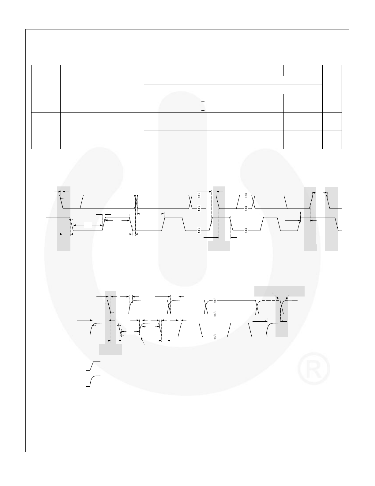
Timing Diagrams
Figure 4. I2C Interface Timing for Fast and Slow Modes
© 2012 Fairchild Semiconductor Corporation www.fairchildsemi.com
FAN54015 • Rev. 1.0.2 9
Figure 5. I2C Interface Timing for High-Speed Mode
FAN54015 — USB-Compliant Single-Cell Li-Ion Switching Charger with USB-OTG Boost Regulator
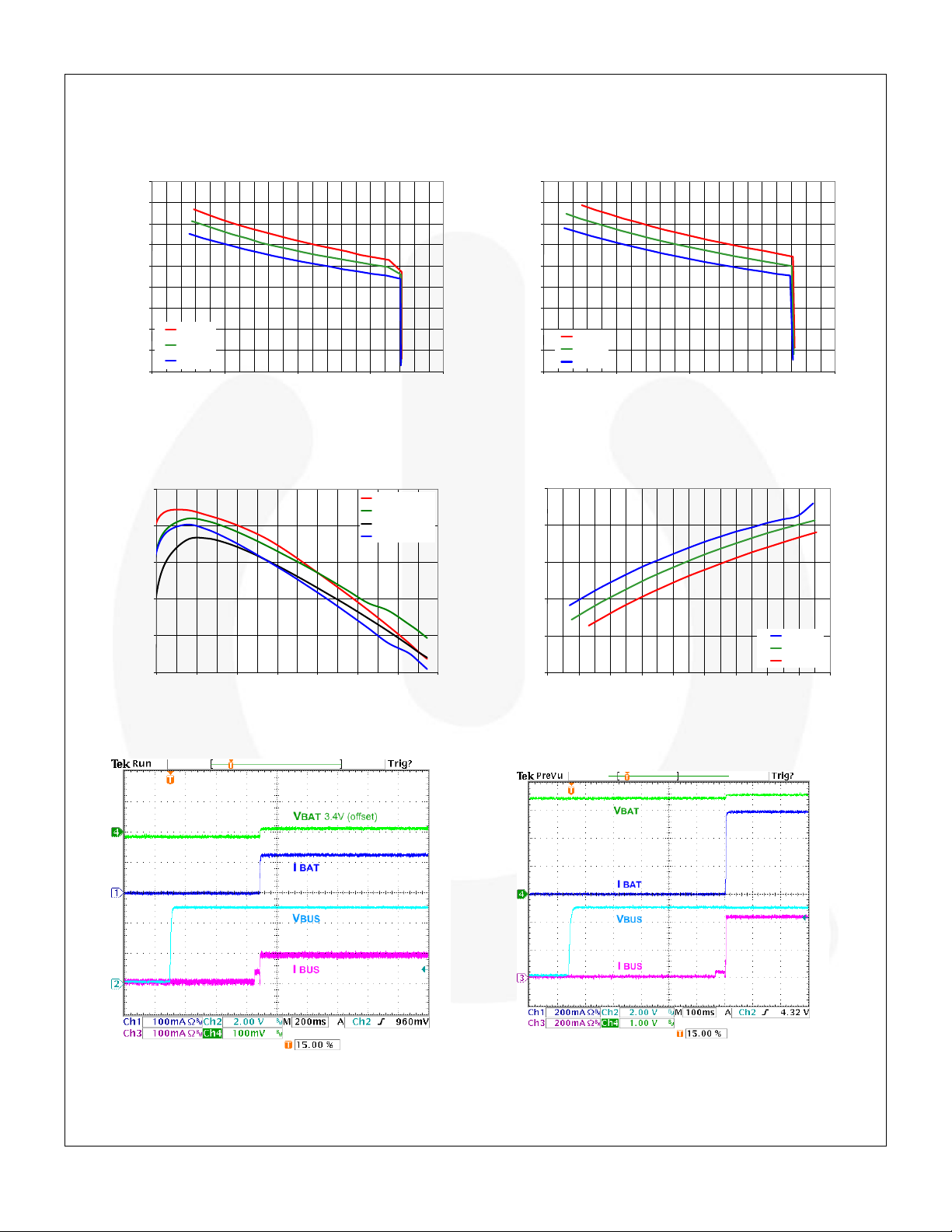
Charge Mode Typical Characteristics
Unless otherwise specified, circuit of Figure 1, V
OREG
=4.2 V, V
BUS
=5.0 V, and TA=25°C.
Figure 6. Battery Charge Current vs. V
BUS
with
I
INLIM
=100 mA
Figure 7. Battery Charge Current vs. V
BUS
with
I
INLIM
=500 mA
Figure 8. Charger Efficiency, No I
INLIM
, I
OCHARGE
=1450 mA
Figure 9. Charger Efficiency vs. V
BUS
, I
INLIM
=500 mA
Figure 10. Auto-Charge Startup at VBUS Plug-in,
I
INLIM
=100 mA, OTG=1, V
BAT
=3.4 V
Figure 11. Auto-Charge Startup at VBUS Plug-in,
I
INLIM
=500 mA, OTG=1, V
BAT
=3.4 V
-
20
40
60
80
100
120
140
160
180
2.5 3 3.5 4 4.5
Battery Charge Current (mA)
Battery Voltage, VBAT (V)
5.5VBUS
5.0VBUS
4.5VBUS
-
100
200
300
400
500
600
700
800
900
2.5 3 3.5 4 4.5
Battery Charge Current (mA)
Battery Voltage, VBAT (V)
5.5VBUS
5.0VBUS
4.5VBUS
82%
85%
88%
91%
94%
97%
100 300 500 700 900 1100 1300 1500
Efficiency
Battery Charge Current (mA)
4.20VBAT, 4.5VBUS
4.20VBAT, 5.0VBUS
3.54VBAT, 5.0VBUS
3.54VBAT, 4.5VBUS
84%
86%
88%
90%
92%
94%
2.5 2.7 2.9 3.1 3.3 3.5 3.7 3.9 4.1 4.3
Efficiency
Battery Voltage, VBAT (V)
4.5VBUS
5.0VBUS
5.5VBUS
© 2012 Fairchild Semiconductor Corporation www.fairchildsemi.com
FAN54015 • Rev. 1.0.2 10
FAN54015 — USB-Compliant Single-Cell Li-Ion Switching Charger with USB-OTG Boost Regulator
Charge Mode Typical Characteristics
Unless otherwise specified, circuit of Figure 1, V
OREG
=4.2 V, V
BUS
=5.0 V, and TA=25°C.
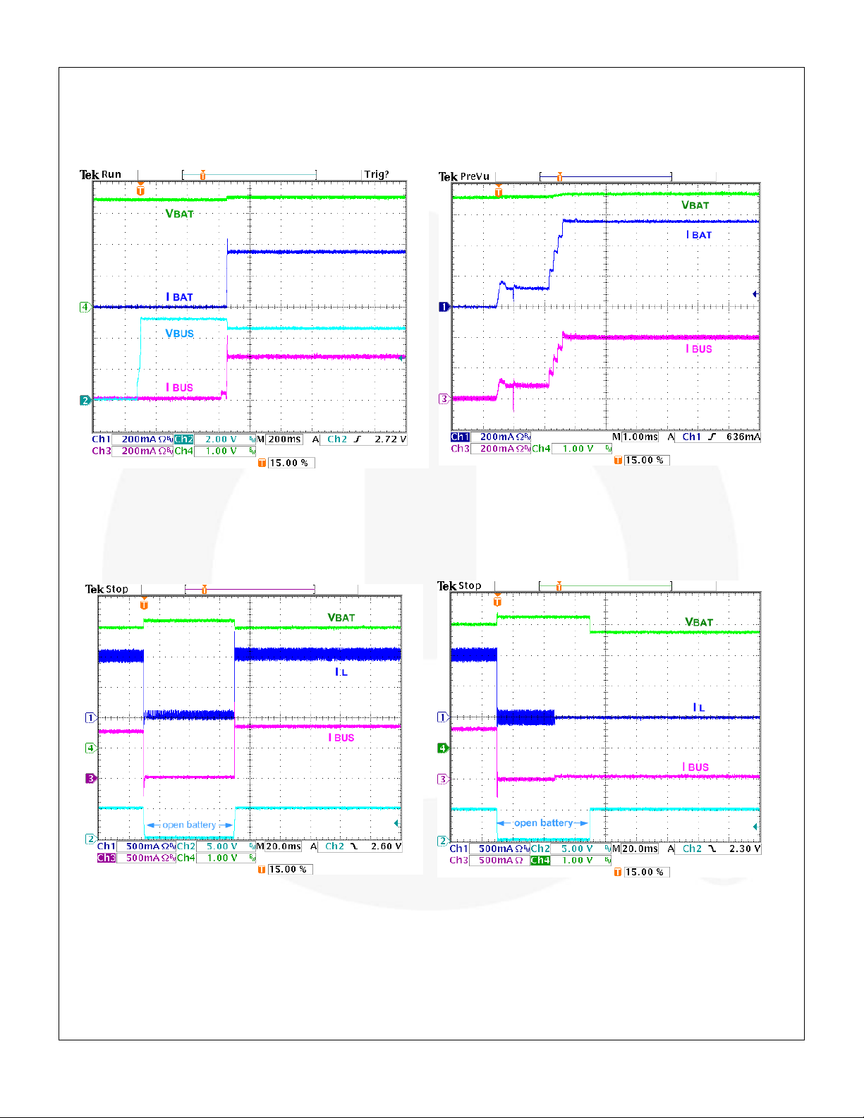
Figure 12. AutoCharge Startup with 300mA Limited
Charger / Adaptor, I
INLIM
=500 mA, OTG=1, V
BAT
=3.4 V
Figure 13. Charger Startup with HZ_MODE Bit Reset,
I
INLIM
=500 mA, I
OCHARGE
=1050 mA, OREG=4.2 V, V
BAT
=3.6 V
Figure 14. Battery Removal / Insertion During Charging,
V
BAT
=3.9 V, I
OCHARGE
=1050 mA, No I
INLIM,
TE=0
Figure 15. Battery Removal / Insertion During Charging,
V
BAT
=3.9 V, I
OCHARGE
=1050 mA, No I
INLIM,
TE=1
© 2012 Fairchild Semiconductor Corporation www.fairchildsemi.com
FAN54015 • Rev. 1.0.2 11

FAN54015 — USB-Compliant Single-Cell Li-Ion Switching Charger with USB-OTG Boost Regulator
Charge Mode Typical Characteristics
Unless otherwise specified, circuit of Figure 1, V
OREG
=4.2 V, V
BUS
=5.0 V, and TA=25°C.
Figure 16. VBUS Current in High-Impedance Mode
with Battery Open
Figure 17. V
REG
1.8 V Output Regulation
Figure 18. No Battery, V
BUS
at Power Up
0
50
100
150
200
4.0 4.5 5.0 5.5 6.0
High-Z Mode Current (A)
Input Voltage, VBUS (V)
-30C
+25C
+85C
1.77
1.78
1.79
1.80
1.81
1.82
0 1 2 3 4 5
VREG (V)
1.8V Regulator Load Current (mA)
-10C, 5.0VBUS
+25C, 5.0VBUS
+85C, 5.0VBUS
© 2012 Fairchild Semiconductor Corporation www.fairchildsemi.com
FAN54015 • Rev. 1.0.2 12

FAN54015 — USB-Compliant Single-Cell Li-Ion Switching Charger with USB-OTG Boost Regulator
Boost Mode Typical Characteristics
Unless otherwise specified, using circuit of Figure 1, V
BAT
=3.6 V, TA=25°C.
Figure 19. Efficiency vs. V
BAT
Figure 20. Efficiency Over Temperature
Figure 21. Output Regulation vs. V
BAT
Figure 22. Output Regulation Over Temperature
Figure 23. Quiescent Current
Figure 24. High-Impedance Mode Battery Current
75
80
85
90
95
100
0 100 200 300 400 500
Efficiency (%)
VBUS Load Current (mA)
3.0 VBAT
3.6 VBAT
4.2 VBAT
75
80
85
90
95
100
0 100 200 300 400 500
Efficiency (%)
VBUS Load Current (mA)
-10C, 3.6VBAT
+25C, 3.6VBAT
+85C, 3.6VBAT
4.80
4.85
4.90
4.95
5.00
5.05
5.10
0 100 200 300 400 500
VBUS (V)
VBUS Load Current (mA)
3.0 VBAT
3.6 VBAT
4.2 VBAT
4.80
4.85
4.90
4.95
5.00
5.05
5.10
0 100 200 300 400 500
VBUS (V)
VBUS Load Current (mA)
-10C, 3.6VBAT
+25C, 3.6VBAT
+85C, 3.6VBAT
50
100
150
200
250
2 2.5 3 3.5 4 4.5 5
Quiescent Current (µA)
Battery Voltage, VBAT (V)
-30C
+25C
+85C
0
5
10
15
20
2 2.5 3 3.5 4 4.5 5
High-Z Mode Current (µA)
Battery Voltage, VBAT (V)
-30C
+25C
+85C
© 2012 Fairchild Semiconductor Corporation www.fairchildsemi.com
FAN54015 • Rev. 1.0.2 13

FAN54015 — USB-Compliant Single-Cell Li-Ion Switching Charger with USB-OTG Boost Regulator
Boost Mode Typical Characteristics
Unless otherwise specified, using circuit of Figure 1, V
BAT
=3.6 V, TA=25°C.
Figure 25. Boost PWM Waveform
Figure 26. Boost PFM Waveform
Figure 27. Output Ripple vs. V
BAT
Figure 28. Output Ripple vs. Temperature
0
5
10
15
20
25
30
0 100 200 300 400 500
VBUS Ripple (mVpp)
VBUS Load Current (mA)
2.7 VBAT
3.6 VBAT
4.2 VBAT
4.5 VBAT
0
5
10
15
20
25
30
0 100 200 300 400 500
VBUS Ripple (mVpp)
VBUS Load Current (mA)
-30C, 3.6VBAT
+25C, 3.6VBAT
+85C, 3.6VBAT
© 2012 Fairchild Semiconductor Corporation www.fairchildsemi.com
FAN54015 • Rev. 1.0.2 14

FAN54015 — USB-Compliant Single-Cell Li-Ion Switching Charger with USB-OTG Boost Regulator
Boost Mode Typical Characteristics
Unless otherwise specified, using circuit of Figure 1, V
BAT
=3.6 V, TA=25°C.
Figure 29. Startup, 3.6 V
BAT
, 44 Load, Additional 10 µF,
X5R Across V
BUS
Figure 30. V
BUS
Fault Response, 3.6 V
BAT
Figure 31. Load Transient, 5-155-5 mA, tR=tF=100 ns
Figure 32. Load Transient, 5-255-5 mA, tR=tF=100 ns
IBAT
I
L
V
BUS
© 2012 Fairchild Semiconductor Corporation www.fairchildsemi.com
FAN54015 • Rev. 1.0.2 15

FAN54015 — USB-Compliant Single-Cell Li-Ion Switching Charger with USB-OTG Boost Regulator
V
OREG
V
BAT
I
SHORT
I
CHARGE
PRE-
CHARGE
CONSTANT CURRENT
(CC)
CONSTANT
VOLTAGE (CV)
V
SHORT
I
TERM
I
SHORT
V
SHORT
V
OREG
V
OREG
I
SHORT
I
C
H
A
R
G
E
PRE-
CHARGE
CURRENT REGULATION
VOLTAGE
REGULATION
V
SHORT
I
TERM
V
B
A
T
Circuit Description / Overview
When charging batteries with a current-limited input source,
such as USB, a switching charger’s high efficiency over a
wide range of output voltages minimizes charging time.
FAN54015 combines a highly integrated synchronous buck
regulator for charging with a synchronous boost regulator,
which can supply 5 V to USB On-The-Go (OTG) peripherals.
The regulator employs synchronous rectification for both the
charger and boost regulators to maintain high efficiency over
a wide range of battery voltages and charge states.
The FAN54015 has three operating modes:
1. Charge Mode:
Charges a single-cell Li-ion or Li-polymer battery.
2. Boost Mode:
Provides 5 V power to USB-OTG with an integrated
synchronous rectification boost regulator using the
battery as input.
3. High-Impedance Mode:
Both the boost and charging circuits are OFF in this
mode. Current flow from VBUS to the battery or from the
battery to VBUS is blocked in this mode. This mode
consumes very little current from VBUS or the battery.
Note: Default settings are denoted by bold typeface.
The FAN54015 is designed to work with a current-limited
input source at VBUS. During the current regulation phase
of charging, I
or the programmed charging current
INLIM
limits the amount of current available to charge the battery
and power the system. The effect of I
INLIM
on I
CHARGE
can be
seen in Figure 34.
Figure 33. Charge Curve, I
Not Limited by I
CHARGE
INLIM
Charge Mode
In Charge Mode, FAN54015 employs four regulation loops:
1. Input Current: Limits the amount of current drawn from
VBUS. This current is sensed internally and can be
programmed through the I2C interface.
2. Charging Current: Limits the maximum charging current.
This current is sensed using an external R
3. Charge Voltage: The regulator is restricted from
exceeding this voltage. As the internal battery voltage
rises, the battery’s internal impedance and R
in conjunction with the charge voltage regulation to
decrease the amount of current flowing to the battery.
Battery charging is completed when the voltage across
R
drops below the I
SENSE
4. Temperature: If the IC’s junction temperature reaches
120°C, charge current is reduced until the IC’s
temperature stabilizes at 120°C.
5. An additional loop limits the amount of drop on VBUS to
a programmable voltage (VSP) to accommodate “special
chargers” that limit current to a lower current than might
be available from a “normal” USB wall charger.
Battery Charging Curve
If the battery voltage is below V
pre-charges the battery until V
charging circuit is then started and the battery is charged
with a constant current if sufficient input power is available.
The current slew rate is limited to prevent overshoot.
threshold.
TERM
SHORT
reaches V
BAT
, a linear current source
SHORT
resistor.
SENSE
SENSE
. The PWM
work
Figure 34. Charge Curve, I
INLIM
Limits I
CHARGE
Assuming that V
is programmed to the cell’s fully
OREG
charged “float” voltage, the current that the battery accepts
with the PWM regulator limiting its output (sensed at VBAT)
to V
declines, and the charger enters the voltage
OREG
regulation phase of charging. When the current declines to
the programmed I
value, the charge cycle is complete.
TERM
Charge current termination can be disabled by resetting the
TE bit (REG1[3]).
The charger output or “float” voltage can be programmed by
the OREG bits from 3.5 V to 4.44 V in 2 0mV increments, as
shown in Table 3.
© 2012 Fairchild Semiconductor Corporation www.fairchildsemi.com
FAN54015 • Rev. 1.0.2 16

FAN54015 — USB-Compliant Single-Cell Li-Ion Switching Charger with USB-OTG Boost Regulator
Decimal
Hex
VOREG
Decimal
Hex
VOREG
0
00
3.50 32
20
4.14
1
01
3.52 33
21
4.16
2
02
3.54
34
22
4.18
3
03
3.56 35
23
4.20
4
04
3.58 36
24
4.22
5
05
3.60 37
25
4.24
6
06
3.62 38
26
4.26
7
07
3.64 39
27
4.28
8
08
3.66 40
28
4.30
9
09
3.68 41
29
4.32
10
0A
3.70 42
2A
4.34
11
0B
3.72 43
2B
4.36
12
0C
3.74 44
2C
4.38
13
0D
3.76 45
2D
4.40
14
0E
3.78 46
2E
4.42
15
0F
3.80 47
2F
4.44
16
10
3.82 48
30
4.44
17
11
3.84 49
31
4.44
18
12
3.86 50
32
4.44
19
13
3.88 51
33
4.44
20
14
3.90 52
34
4.44
21
15
3.92 53
35
4.44
22
16
3.94 54
36
4.44
23
17
3.96 55
37
4.44
24
18
3.98 56
38
4.44
25
19
4.00 57
39
4.44
26
1A
4.02 58
3A
4.44
27
1B
4.04 59
3B
4.44
28
1C
4.06 60
3C
4.44
29
1D
4.08 61
3D
4.44
30
1E
4.10 62
3E
4.44
Parameter
Name
Register
Output Voltage Regulation
V
OREG
REG2[7:2]
Battery Charging Current Limit
I
OCHRG
REG4[6:4]
Input Current Limit
I
INLIM
REG1[7:6]
Charge Termination Limit
I
TERM
REG4[2:0]
Weak Battery Voltage
V
LOWV
REG1[5:4]
DEC
BIN
HEX
V
RSENSE
(mV)
I
OCHARGE
(mA)
68 m
100 m
0
000
00
37.4
550
374
1
001
01
44.2
650
442 2 010
02
51.0
750
510
3
011
03
57.8
850
578
4
100
04
71.4
1050
714
5
101
05
78.2
1150
782
6
110
06
91.8
1350
918
7
111
07
98.6
1450
986
I
TERM
V
RSENSE
(mV)
I
TERM
(mA)
68 m
100 m
0
3.3
49
33
1
6.6
97
66
2
9.9
146
99 3 13.2
194
132 4 16.5
243
165 5 19.8
291
198 6 23.1
340
231 7 26.4
388
264
CE
Table 3. OREG Bits (OREG[7:2]) vs. Charger V
(V
) Float Voltage
OREG
OUT
A new charge cycle begins when one of the following occurs:
The battery voltage falls below V
OREG
- V
RCH
VBUS Power on Reset (POR) clears and the battery
voltage is below the weak battery threshold (V
LOWV
).
or HZ_MODE is reset through I2C write to
CONTROL1 (R1) register.
Charge Current Limit (I
Table 5. I
of I
OCHARGE
OCHARGE
Bits and R
(REG4 [6:4]) Current as Function
SENSE
OCHARGE
Resistor Values
)
Termination Current Limit
Current charge termination is enabled when TE (REG1[3])=1.
Typical termination current values are given in Table 6.
Table 6. I
(REG4[2:0]) and R
Current as Function of I
TERM
Resistor Values
SENSE
TERM
Bits
The following charging parameters can be programmed by
the host through I2C:
Table 4. Programmable Charging Parameters
© 2012 Fairchild Semiconductor Corporation www.fairchildsemi.com
FAN54015 • Rev. 1.0.2 17
When the charge current falls below I
, PWM charging
TERM
stops and the STAT bits change to READY (00) for about
500 ms while the IC determines whether the battery and
charging source are still connected. STAT then changes to
CHARGE DONE (10), provided the battery and charger are
still connected.

FAN54015 — USB-Compliant Single-Cell Li-Ion Switching Charger with USB-OTG Boost Regulator
I
INLIM
REG1[7:6]
Input Current Limit
00
100 mA
01
500 mA
10
800 mA
11
No limit
CE
PWM Controller in Charge Mode
The IC uses a current-mode PWM controller to regulate the
output voltage and battery charge currents. The synchronous
rectifier (Q2) has a current limit that which off the FET when
the current is negative by more than 140mA peak. This
prevents current flow from the battery.
Safety Timer
Section references Figure 39.
At the beginning of charging, the IC starts a 15-minute timer
(t
). When this times out, charging is terminated. Writing
15MIN
to any register through I2C stops and resets the t
which in turn starts a 32-second timer (t
TMR_RST bit (REG0[7]) resets the t
timer. If the t
32S
). Setting the
32S
times out; charging is terminated, the registers are set to
their default values, and charging resumes using the default
values with the t
timer running.
15MIN
Normal charging is controlled by the host with the t
running to ensure that the host is alive. Charging with the
t
timer running is used for charging that is unattended by
15MIN
the host. If the t
timer expires; the IC turns off the
15MIN
charger, sets the bit, and indicates a timer fault (110) on
the FAULT bits (REG0[2:0]). This sequence prevents
overcharge if the host fails to reset the t
V
POR / Non-Compliant Charger Rejection
BUS
When the IC detects that V
has risen above V
BUS
32S
timer.
15MIN
32S
timer,
timer
32S
timer
IN(MIN)1
USB-Friendly Boot Sequence
At VBUS POR, when the battery voltage is above the weak
battery threshold (V
its I2C register settings. If V
), the IC operates in accordance with
LOWV
BAT
< V
, the IC sets all
LOWV
registers to their default values and enables the charger
using an input current limit controlled by the OTG pin
(100mA if OTG is LOW and 500 mA if OTG is HIGH). This
feature can revive a battery whose voltage is too low to
ensure reliable host operation. Charging continues in the
absence of host communication even after the battery has
reached V
charger remains active until t
, whose default value is 3.54 V, and the
OREG
times out. Once the host
15MIN
processor begins writing to the IC, charging parameters are
set by the host, which must continually reset the t
32S
continue charging using the programmed charging
parameters. If t
.times out, the register defaults are loaded,
32S
the FAULT bits are set to 110, STAT is pulsed HIGH, and
charging continues with default charge parameters.
Input Current Limiting
To minimize charging time without overloading VBUS current
limitations, the IC’s input current limit can be programmed by
the I
Table 7. Input Current Limit
bits (REG1[7:6]).
INLIM
timer to
(4.4 V), the IC applies a 100 load from VBUS to GND. To
clear the VBUS POR (Power-On-Reset) and begin charging,
VBUS must remain above V
t
VBUS_VALID
(30 ms) before the IC initiates charging. The
VBUS validation sequence always occurs before charging is
initiated or re-initiated (for example, after a VBUS OVP fault
or a V
t
VBUS_VALID
recharge initiation).
RCH
ensures that unfiltered 50 / 60 Hz chargers and
and below VBUS
IN(MIN)1
OVP
for
The OTG pin establishes the input current limit when t
running.
15MIN
is
other non-compliant chargers are rejected.
© 2012 Fairchild Semiconductor Corporation www.fairchildsemi.com
FAN54015 • Rev. 1.0.2 18

FAN54015 — USB-Compliant Single-Cell Li-Ion Switching Charger with USB-OTG Boost Regulator
VBUS POR
V
BAT
> V
LOWV
YES
Charge
Configuration
State
T15Min Timer?
NO
NO
YES
NO
Reset all registers
Start T
15MIN
NO
YES
HZ State
YES
Charge State
NO
YES
HZ State
NO
YES
T32Sec
Armed?
NO
YES
T32Sec
Armed?
HZ, CE# or
DISABLE Pin
set?
CE
HZ, CE# or
DISABLE Pin
set?
CE
HZ, CE# or
DISABLE Pin
set?
CE
Flow Charts
Figure 35. Charger VBUS POR
© 2012 Fairchild Semiconductor Corporation www.fairchildsemi.com
FAN54015 • Rev. 1.0.2 19

FAN54015 — USB-Compliant Single-Cell Li-Ion Switching Charger with USB-OTG Boost Regulator
CHARGE STATE
YES
YES
Disable Charging
Indicate
VBUS Fault
NO
T
15MIN
Timeout?
NO
Enable I
SHORT
,
Reset Safety reg
Indicate Charging
PWM Charging
Indicate Charging
NO
YES
VBUS OK?
YES
Indicate timer fault
Set CE
HIGHZ mode
Indicate Charge
Complete
NO
V
BAT
< V
OREG–VRCH
NO
YES
VBUS OK?
Charge
Configuration
State
YES
NO
Disable Charging
Indicate
VBUS Fault
NO
YES
T
15MIN
Timeout?
NO
I
OUT
< I
TERM
Termination enabled
V
BAT
> V
OREG–VRCH
V
BAT
< V
SHORT
YES
Battery Removed
Reset charge
parameters
V
BAT
< V
OREG–VRCH
Reset Safety reg
Delay t
INT
Stop Charging
Enable IDET for T
DETECT
Flow Charts (Continued)
Figure 36. Charge Mode
© 2012 Fairchild Semiconductor Corporation www.fairchildsemi.com
FAN54015 • Rev. 1.0.2 20

FAN54015 — USB-Compliant Single-Cell Li-Ion Switching Charger with USB-OTG Boost Regulator
Charge
Configuration
State
T32Sec
ARMED AND
CE# = 0?
Charge State
YES
NO
VBAT < VOREG
for 262ms?
NO
YES
NO
YES
START T15Min
Has T15Min
and CE# = 0
CE
CE
Stop T32Sec
HZ State
NO
Charge State
VBAT > VLOWV?
YES
YES
RUN
T32Sec
Reset T15min
if running
DISABLE
PIN
HIGH
LOW
LOW
HIGH
NO
HZ or CE# set?
CE
DISABLE
PIN
Flow Charts (Continued)
Figure 37. Charge Configuration
© 2012 Fairchild Semiconductor Corporation www.fairchildsemi.com
FAN54015 • Rev. 1.0.2 21
Figure 38. HZ-State

FAN54015 — USB-Compliant Single-Cell Li-Ion Switching Charger with USB-OTG Boost Regulator
Charge Start
Start T
15MIN
T
15MIN
Active?
Reset Registers
YES
NO
Start T
32SEC
Stop T
15MIN
I2C Write
received?
YES
T
15MIN
Expired?
NO
Continue
Charging
T
32SEC
Expired?
YES
NO
NO
YES
Timer Fault :
Set CE
CE
Flow Charts (Continued)
Figure 39. Timer Flow Chart
© 2012 Fairchild Semiconductor Corporation www.fairchildsemi.com
FAN54015 • Rev. 1.0.2 22

FAN54015 — USB-Compliant Single-Cell Li-Ion Switching Charger with USB-OTG Boost Regulator
SP (REG5[2:0])
DEC
BIN
HEX
VSP
0
000
00
4.213
1
001
01
4.293
2
010
02
4.373
3
011
03
4.453
4
100
04
4.533
5
101
05
4.613
6
110
06
4.693
7
111
07
4.773
ISAFE (REG6[6:4])
DEC
BIN
HEX
V
RSENSE
(mV)
I
SAFE
(mA)
68 m
100 m
0
000
00
37.4
550
374
1
001
01
44.2
650
442
2
010
02
51.0
750
510
3
011
03
57.8
850
578
4
100
04
71.4
1050
714
5
101
05
78.2
1150
782
6
110
06
91.8
1350
918
7
111
07
98.6
1450
986
VSAFE (REG6[3:0])
DEC
BIN
HEX
Max. OREG
(REG2[7:2])
VOREG
Max.
0
0000
00
100011
4.20
1
0001
01
100100
4.22
2
0010
02
100101
4.24
3
0011
03
100110
4.26
4
0100
04
100111
4.28
5
0101
05
101000
4.30
6
0110
06
101001
4.32
7
0111
07
101010
4.34
8
1000
08
101011
4.36
9
1001
09
101100
4.38
10
1010
0A
101101
4.40
11
1011
0B
101110
4.42
12
1100
0C
101111
4.44
13
1101
0D
110000
4.44
14
1110
0E
110001
4.44
15
1111
0F
110010
4.44
Special Charger
The FAN54015 has additional functionality to limit input
current in case a current-limited “special charger” is
supplying VBUS. These slowly increase the charging current
Table 9. I
Bits (REG6[6:4])
SAFE
(I
OCHARGE
Limit) as Function of ISAFE
until either:
I
INLIM
or I
OCHARGE
is reached
or
V
If V
BUS
BUS=VSP
.
collapses to VSP when the current is ramping up, the
FAN54015 charge with an input current that keeps
V
BUS=VSP
. When the VSP control loop is limiting the charge
current, the SP bit (REG5[4]) is set.
Table 8. VSP as Function of SP Bits (REG5[2:0])
Safety Settings
FAN54015 contain a SAFETY register (REG6) that prevents
the values in OREG (REG2[7:2]) and IOCHARGE
(REG4[6:4]) from exceeding the values of the VSAFE and
ISAFE values.
After V
with its default value and may be written only before any
other register is written. The entire desired Safety register
value should be written twice to ensure the register bits are
set. After writing to any other register, the SAFETY register
is locked until V
The ISAFE (REG6[6:4]) and VSAFE (REG6[3:0]) registers
establish values that limit the maximum values of I
and V
write a value higher than VSAFE or ISAFE to OREG or
IOCHARGE, respectively; the VSAFE, ISAFE value appears
as the OREG, IOCHARGE register value, respectively.
exceeds V
BAT
falls below V
BAT
used by the control logic. If the host attempts to
OREG
, the SAFETY register is loaded
SHORT
.
SHORT
OCHARGE
Table 10. V
SAFE
(V
Limit) as Function of VSAFE
OREG
Bits (REG6[3:0])
Thermal Regulation and Protection
When the IC’s junction temperature reaches T
120°C), the charger reduces its output current to 550 mA to
prevent overheating. If the temperature increases beyond
T
SHUTDOWN
to 101, and STAT is pulsed HIGH. In Suspend Mode, all
timers stop and the state of the IC’s logic is preserved.
Charging resumes at programmed current after the die
cools to about 120°C.
; charging is suspended, the FAULT bits are set
(about
CF
© 2012 Fairchild Semiconductor Corporation www.fairchildsemi.com
FAN54015 • Rev. 1.0.2 23

FAN54015 — USB-Compliant Single-Cell Li-Ion Switching Charger with USB-OTG Boost Regulator
Power (W)
JA
0.504
54°C/W
0.844
50°C/W
1.506
46°C/W
EN_STAT
Charge State
STAT Pin
0 X OPEN
X
Normal Conditions
OPEN
1
Charging
LOW
X
Fault (Charging or Boost)
128s Pulse,
then OPEN
Additional JA data points, measured using the FAN54015
evaluation board, are given in Table 11 (measured with
TA=25°C). Note that as power dissipation increases, the
effective JA decreases due to the larger difference between
the die temperature and ambient.
Battery Detection During Charging
The IC can detect the presence, absence, or removal of a
battery if the termination bit (TE) is set. During normal
charging, once V
is close to V
BAT
and the termination
OREG
charge current is detected, the IC terminates charging and
sets the STAT bits to 10. It then turns on a discharge current,
Table 11. Evaluation Board Measured JA
I
DETECT
, for t
DETECT
. If V
is still above V
BAT
OREG
– V
RCH
, the
battery is present and the IC sets the FAULT bits to 000. If
V
is below V
BAT
OREG
– V
, the battery is absent and the IC:
RCH
1. Sets the registers to their default values.
2. Sets the FAULT bits to 111.
Charge Mode Input Supply Protection
Sleep Mode
When V
V
IN(MIN),
draining into VBUS. During Sleep Mode, reverse current is
falls below V
BUS
BAT
+ V
, and V
SLP
is above
BUS
the IC enters Sleep Mode to prevent the battery from
3. Resumes charging with default values after t
Battery Short-Circuit Protection
If the battery voltage is below the short-circuit threshold
(V
); a linear current source, I
SHORT
V
BAT
> V
SHORT
.
SHORT
, supplies V
System Operation with No Battery
INT
.
until
BAT
disabled by body switching Q1.
The FAN54015 continues charging after VBUS POR with the
Input Supply Low-Voltage Detection
The IC continuously monitors VBUS during charging. If V
falls below V
IN(MIN)
, the IC:
BUS
1. Terminates charging
2. Pulses the STAT pin, sets the STAT bits to 11, and sets
the FAULT bits to 011.
If V
recovers above the V
BUS
t
(about two seconds), the charging process is repeated.
INT
rising threshold after time
IN(MIN)
This function prevents the USB power bus from collapsing or
oscillating when the IC is connected to a suspended USB
port or a low-current-capable OTG device.
Input Over-Voltage Detection
When the V
exceeds VBUS
BUS
, the IC:
OVP
1. Turns off Q3
2. Suspends charging
3. Sets the FAULT bits to 001, sets the STAT bits to 11,
and pulses the STAT pin.
When V
cleared and charging resumes after V
falls about 150 mV below VBUS
BUS
, the fault is
OVP
is revalidated (see
BUS
VBUS POR / Non-Compliant Charger Rejection).
VBUS Short While Charging
If VBUS is shorted with a very low impedance while the IC is
charging with I
=100 mA, the IC may not meet
INLIMIT
datasheet specifications until power is removed. To trigger
this condition, V
must be driven from 5 V to GND with a
BUS
high slew rate. Achieving this slew rate requires a 0 short
to the USB cable less than 10cm from the connector.
Charge Mode Battery Detection & Protection
VBAT Over-Voltage Protection
The OREG voltage regulation loop prevents V
BAT
from
default parameters, regulating the V
the host processor issues commands or the 15-minute timer
line to 3.54 V until
BAT
expires. In this way, the FAN54015 can start the system
without a battery.
The FAN54015 soft-start function can interfere with the
system supply with battery absent. The soft-start activates
whenever V
OREG
, I
INLIM
, or I
OCHARGE
are set from a lower to
higher value. During soft-start, the IIN limit drops to 100 mA
for about 1ms unless I
is set to 11 (no limit). This could
INLIM
cause the system processor to fail to start. To avoid this
behavior, use the following sequence.
1. Set the OTG pin HIGH. When VBUS is plugged in, I
is set to 500 mA until the system processor powers up
and can set parameters through I2C.
2. Program the Safety Register.
3. Set I
to 11 (no limit).
INLIM
4. Set OREG to the desired value (typically 4.18).
5. Reset the IO_LEVEL bit, then set IOCHARGE.
6. Set I
to 500mA if a USB source is connected.
INLIM
During the initial system startup, while the charger IC is
being programmed, the system current is limited to 500mA
for 1ms during steps 4 and 5. This is the value of the softstart ICHARGE current used when I
is set to No Limit.
INLIM
If the system is powered up without a battery present, the
CV bit should be set. When a battery is inserted, the CV bit
is cleared.
Charger Status / Fault Status
The STAT pin indicates the operating condition of the IC and
provides a fault indicator for interrupt driven systems.
Table 12. STAT Pin Function
INLIM
overshooting the OREG voltage by more than 50 mV when
the battery is removed. When the PWM charger runs with no
battery, the TE bit is not set and a battery is inserted that is
charged to a voltage higher than V
; PWM pulses stop. If
OREG
no further pulses occur for 30 ms, the IC sets the FAULT bits
to 100, sets the STAT bits to 11, and pulses the STAT pin.
© 2012 Fairchild Semiconductor Corporation www.fairchildsemi.com
FAN54015 • Rev. 1.0.2 24

FAN54015 — USB-Compliant Single-Cell Li-Ion Switching Charger with USB-OTG Boost Regulator
Fault Bit
Fault Description
B2
B1
B0
0 0 0
Normal (No Fault)
0 0 1
VBUS OVP
0 1 0
Sleep Mode
0 1 1
Poor Input Source
1 0 0
Battery OVP
1 0 1
Thermal Shutdown
1 1 0
Timer Fault
1 1 1
No Battery
Charging
DISABLE Pin
HZ_MODE
ENABLE
0 0 0
DISABLE
X 1 X
DISABLE
X X 1
DISABLE
1 X X
HZ_MODE
OPA_MODE
FAULT
Operation Mode
0 0 0
Charge 0 X
1
Charge Configure
0 1 0
Boost 1 X
X
High Impedance
OTG_EN
OTG
Pin
HZ_
MODE
OPA_
MODE
BOOST
1 X X Enabled
X X 0 1 Enabled
X X
0
Disabled
0 X 1 X Disabled
1 1 1 Disabled
0 0 0 Disabled
CECECE
CE
CE
CE
ACTIVE
ACTIVE
ACTIVE
ACTIVE
The FAULT bits (R0[2:0]) indicate the type of fault in Charge
Mode (see Table 13).
Table 15. Operation Mode Control
Table 13. Fault Status Bits During Charge Mode
The IC resets the OPA_MODE bit whenever the boost is
deactivated, whether due to a fault or being disabled by
setting the HZ_MODE bit.
Boost Mode
Boost Mode can be enabled if the IC is in 32-Second Mode
with the OTG pin and OPA_MODE bits as indicated in Table
16. The OTG pin ACTIVE state is 1 if OTG_PL=1 and 0
when OTG_PL=0.
Charge Mode Control Bits
Setting either HZ_MODE or through I2C disables the
charger and puts the IC into High-Impedance Mode and
resets t
t
32S
(except SAFETY) reset, which enables t
versions with the 15-minute timer.
When t
enters High-Impedance Mode. If was set by t
overflow, a new charge cycle can only be initiated through
I2C or VBUS POR.
Setting the RESET bit clears all registers. If HZ_MODE or
also cleared, but the t
remains in High-Impedance Mode.
Table 14. DISABLE Pin and Bit Functionality
32S
. If V
BAT
< V
while in High-Impedance Mode,
LOWV
begins running and, when it overflows, all registers
charging on
15MIN
overflows, the IC sets the bit and the IC
15MIN
15MIN
bits were set when the RESET bit is set, these bits are
timer is not started, and the IC
32S
If boost is active using the OTG pin, Boost Mode is initiated
even if the HZ_MODE=1. The HZ_MODE bit overrides the
OPA_MODE bit.
Table 16. Enabling Boost
To remain in Boost Mode, the TMR_RST must be set by the
host before the t
Mode; the IC resets all registers, pulses the STAT pin, sets
the FAULT bits to 110, and resets the BOOST bit. VBUS
POR or reading R0 clears the fault condition.
timer times out. If t
32S
times out in Boost
32S
Raising the DISABLE pin stops t
does not reset it. If the DISABLE pin is raised during t
charging, the t
Operational Mode Control
OPA_MODE (REG1[0]) and the HZ_MODE (REG1[1]) bits in
conjunction with the FAULT state define the operational
mode of the charger.
© 2012 Fairchild Semiconductor Corporation www.fairchildsemi.com
FAN54015 • Rev. 1.0.2 25
timer is reset.
15MIN
from advancing, but
32S
15MIN
Boost PWM Control
The IC uses a minimum on-time and computed minimum offtime to regulate VBUS. The regulator achieves excellent
transient response by employing current-mode modulation.
This technique causes the regulator to exhibit a load line.
During PWM Mode, the output voltage drops slightly as the
input current rises. With a constant V
constant output resistance.
The “droop” caused by the output resistance when a load is
applied allows the regulator to respond smoothly to load
transients with no undershoot from the load line. This can be
seen in Figure 31 and Figure 40.
, this appears as a
BAT

FAN54015 — USB-Compliant Single-Cell Li-Ion Switching Charger with USB-OTG Boost Regulator
LOADOUTOUT
IR07.5V
EQ. 1
V018.52.026.007.5V
OUT
EQ. 1A
V005.52.0327.007.5V
OUT
EQ. 1B
Mode
Description
Invoked When
LIN
Linear Startup
V
BAT
> V
BUS
SS
Boost Soft-Start
V
BUS
< V
BST
BST
Boost Operating Mode
V
BAT
> UVLO
BST
and
SS Completed
Fault Bit
Fault Description
B2
B1
B0
0 0 0
Normal (no fault)
0 0 1
V
BUS
> VBUS
OVP
0 1 0
V
BUS
fails to achieve the voltage required to
advance to the next state during soft-start
or sustained (>50 s) current limit during the
BST state.
0 1 1
V
BAT
< UVLO
BST
1 0 0
N/A: This code does not appear.
1 0 1
Thermal shutdown
1 1 0
Timer fault; all registers reset.
1 1 1
N/A: This code does not appear.
200
225
250
275
300
325
350
2.0 2.5 3.0 3.5 4.0 4.5 5.0
Battery Voltage, VBAT (V)
Output Resistance (m
W
)
OUT
IN
V
V
SS State
When PMID > V
switching with a reduced peak current limit of about 50% of
its normal current limit. The output slews up until V
within 5% of its setpoint; at which time, the regulation loop is
closed and the current limit is set to 100%.
If the output fails to achieve 95% of its setpoint (V
128 s, the current limit is increased to 100%. If the output
fails to achieve 95% of its setpoint after this second 384s
period, a fault state is initiated.
– 400 mV, the boost regulator begins
BAT
BST
is
BUS
) within
BST State
This is the normal operating mode of the regulator. The
Figure 40. Output Resistance (R
OUT
)
V
as a function of I
BUS
can be computed when the
LOAD
regulator is in PWM Mode (continuous conduction) as:
At V
=3.3 V, and I
BAT
=200 mA, V
LOAD
would drop to:
BUS
regulator uses a minimum t
scheme. The minimum t
OFF
keeps the regulator’s switching frequency reasonably
constant in CCM. t
ON(MIN)
higher value if the inductor current reached 0 before t
in the prior cycle.
To ensure the VBUS does not pump significantly above the
regulation point, the boost switch remains off as long as
FB > V
REF
.
-minimum tON modulation
OFF
is proportional to , which
is proportional to V
and is a
BAT
OFF(MIN)
At V
=2.7 V, and I
BAT
=200 mA, V
LOAD
would drop to:
BUS
PFM Mode
If V
> VREF
BUS
(nominally 5.07 V) when the minimum
BOOST
off-time has ended, the regulator enters PFM Mode. Boost
pulses are inhibited until V
< VREF
BUS
. The minimum
BOOST
on-time is increased to enable the output to pump up
sufficiently with each PFM boost pulse. Therefore the
regulator behaves like a constant on-time regulator, with the
bottom of its output voltage ripple at 5.07 V in PFM Mode.
Table 17. Boost PWM Operating States
Startup
When the boost regulator is shut down, current flow is
prevented from V
V
BUS
to V
BAT
.
BAT
to V
, as well as reverse flow from
BUS
Boost Faults
If a BOOST fault occurs:
1. The STAT pin pulses.
2. OPA_MODE bit is reset.
3. The power stage is in High-Impedance Mode.
4. The FAULT bits (REG0[2:0]) are set per Table 18.
Restart After Boost Faults
If boost was enabled with the OPA_MODE bit and
OTG_EN=0, Boost Mode can only be enabled through
subsequent I2C commands since OPA_MODE is reset on
boost faults. If OTG_EN=1 and the OTG pin is still ACTIVE
(see Table 16), the boost restarts after a 5.2 ms delay, as
shown in Figure 41. If the fault condition persists, restart is
attempted every 5ms until the fault clears or an I2C
command disables the boost.
Table 18. Fault Bits During Boost Mode
LIN State
When EN rises, if V
attempts to bring PMID within 400 mV of V
internal 450 mA current source from VBAT (LIN State). If
PMID has not achieved V
FAULT state is initiated.
© 2012 Fairchild Semiconductor Corporation www.fairchildsemi.com
FAN54015 • Rev. 1.0.2 26
BAT
> UVLO
BAT
, the regulator first
BST
using an
BAT
– 400 mV after 560 s, a

FAN54015 — USB-Compliant Single-Cell Li-Ion Switching Charger with USB-OTG Boost Regulator
BIT#
NAME
STATE
Active When
0
1
MONITOR Address 10H
7
ITERM_CMP
V
CSIN
– V
BAT
< V
ITERM
V
CSIN
– V
BAT
> V
ITERM
Charging with TE=1
V
CSIN
– V
BAT
< 1 mV
V
CSIN
– V
BAT
> 1mV
Charging with TE=0
6
VBAT_CMP
V
BAT
< V
SHORT
V
BAT
> V
SHORT
Charging
V
BAT
< V
LOWV
V
BAT
> V
LOWV
High-Impedance Mode
V
BAT
< UVLO
BST
V
BAT
> UVLO
BST
Boosting
5
LINCHG
Linear Charging Not Enabled
Linear Charging Enabled
Charging
4
T_120
TJ < 120°C
TJ > 120°C
3
ICHG
Charging Current Controlled by
I
CHARGE
Control Loop
Charging Current Not Controlled by
I
CHARGE
Control Loop
Charging
2
IBUS
I
BUS
Limiting Charging Current
Charge Current Not Limited by I
BUS
Charging
1
VBUS_VALID
V
BUS
Not Valid
V
BUS
is Valid
V
BUS
> V
BAT
0
CV
Constant Current Charging
Constant Voltage Charging
Charging
450mA
VBUS
BATTERY
CURRENT
0
560
BOOST
0
64
5200
can supply up to 2 mA. This circuit, which is powered from
PMID, is enabled only when PMID > V
current from the battery. During boost, V
off when the HZ_MODE bit (REG1[1])=1.
and does not drain
BAT
is off. It is also
REG
Monitor Register (Reg10H)
Additional status monitoring bits enable the host processor
Figure 41. Boost Response Attempting to Start into V
BUS
Short Circuit (Times in s)
VREG Pin
The 1.8 V regulated output on this pin can be disabled
through I2C by setting the DIS_VREG bit (REG5[6]). VREG
Table 19. MONITOR Register Bit Definitions
to have more visibility into the status of the IC. The monitor
bits are real-time status indicators and are not internally
debounced or otherwise time qualified.
The state of the MONITOR register bits listed in HighImpedance Mode is only valid when V
is valid.
BUS
© 2012 Fairchild Semiconductor Corporation www.fairchildsemi.com
FAN54015 • Rev. 1.0.2 27

FAN54015 — USB-Compliant Single-Cell Li-Ion Switching Charger with USB-OTG Boost Regulator
Part Type
7 6 5 4 3 2 1
0
FAN54015
1 1 0 1 0 1 0
Symbol
Definition
S
START, see Figure 43
A
ACK. The slave drives SDA to 0 to acknowledge
the preceding packet.
NACK. The slave sends a 1 to NACK the
preceding packet.
R
Repeated START, see Figure 45
P
STOP, see Figure 44. Figure 44
WR/
SCL
T
SU
T
H
SDA
Data change allowed
SCL
T
HD;STA
SDA
Slave Address
MS Bit
SCL
SDA
Slave Releases Master Drives
ACK(0) or
NACK(1)
t
HD;STO
SCL
SDA
ACK(0) or
NACK(1)
Slave Releases
SLADDR
MS Bit
t
HD;STA
t
SU;STA
Master Drives Bus
Slave Drives Bus
A
I2C Interface
The FAN54015’s serial interface is compatible with
Standard, Fast, Fast Plus, and High-Speed Mode I2C-Bus®
specifications. The SCL line is an input and the SDA line is a
bi-directional open-drain output; it can only pull down the bus
when active. The SDA line only pulls LOW during data reads
and signaling ACK. All data is shifted in MSB (bit 7) first.
Slave Address
Table 20. I2C Slave Address Byte
In hex notation, the slave address assumes a 0 LSB. The
hex slave address for the FAN54015 is D4H and is D6H for
all other parts in the family.
Bus Timing
As shown in Figure 42, data is normally transferred when
SCL is LOW. Data is clocked in on the rising edge of SCL.
Typically, data transitions shortly at or after the falling edge
of SCL to allow ample time for the data to set up before the
next SCL rising edge.
During a read from the FAN54015 (Figure 46, Figure 47), the
master issues a Repeated Start after sending the register
address and before resending the slave address. The
Repeated Start is a 1-to-0 transition on SDA while SCL is
HIGH, as shown in Figure 45.
High-Speed (HS) Mode
The protocols for High-Speed (HS), Low-Speed (LS), and
Fast-Speed (FS) Modes are identical except the bus speed for
HS Mode is 3.4 MHz. HS Mode is entered when the bus
master sends the HS master code 00001XXX after a start
condition. The master code is sent in Fast or Fast Plus Mode
(less than 1 MHz clock); slaves do not ACK this transmission.
The master then generates a repeated start condition
(Figure 45) that causes all slaves on the bus to switch to HS
Mode. The master then sends I2C packets, as described
above, using the HS Mode clock rate and timing.
The bus remains in HS Mode until a stop bit (Figure 44) is
sent by the master. While in HS Mode, packets are
separated by repeated start conditions (Figure 45).
Figure 42. Data Transfer Timing
Each bus transaction begins and ends with SDA and SCL
HIGH. A transaction begins with a START condition, which is
defined as SDA transitioning from 1 to 0 with SCL HIGH, as
shown in Figure 43.
Figure 43. Start Bit
A transaction ends with a STOP condition, which is defined
as SDA transitioning from 0 to 1 with SCL HIGH, as shown
in Figure 44.
Figure 44. Stop Bit
Figure 45. Repeated Start Timing
Read and Write Transactions
The figures below outline the sequences for data read and
write. Bus control is signified by the shading of the packet,
defined as and .
All addresses and data are MSB first.
Table 21. Bit Definitions for Figure 46, Figure 47,
and Figure 48
© 2012 Fairchild Semiconductor Corporation www.fairchildsemi.com
FAN54015 • Rev. 1.0.2 28

FAN54015 — USB-Compliant Single-Cell Li-Ion Switching Charger with USB-OTG Boost Regulator
Register
Address Bits
Name
REG#
7 6 5 4 3 2 1
0
CONTROL0
0
0 0 0 0 0 0 0
0
CONTROL1
1
0 0 0 0 0 0 0
1
OREG
2
0 0 0 0 0 0 1
0
IC_INFO
03
or
3BH
0 0 0 0 0 0 1
1
IBAT
4
0 0 0 0 0 1 0
0
SP_CHARGER
5
0 0 0 0 0 1 0
1
SAFETY
6
0 0 0 0 0 1 1
0
MONITOR
10h
0 0 0 0 1 0 1
0
Table 23. Register Bit Definitions
This table defines the operation of each register bit for all IC versions. Default values are in bold text.
Bit
Name
Value
Type
Description
CONTROL0
Register Address: 00
Default Value=X1XX 0XXX
7
TMR_RST
OTG
1
W
Writing a 1 resets the t
32S
timer; writing a 0 has no effect
R
Returns the OTG pin level (1=HIGH)
6
EN_STAT
0
R/W
Prevents STAT pin from going LOW during charging; STAT pin still pulses to
enunciate faults
1
Enables STAT pin LOW when IC is charging
5:4
STAT
00
R
Ready
01
Charge in progress
10
Charge done
11
Fault
3
BOOST
0
R
IC is not in Boost Mode
1
IC is in Boost Mode
2:0
FAULT
R
Fault status bits: for Charge Mode, see Table 13; for Boost Mode, see Table 18
Continued on the following page…
S Slave Address A Reg Addr A A P0
7 bits 8 bits 8 bits
Data
0 0 0
S Slave Address A Reg Addr A0
7 bits 8 bits
R Slave Address
7 bits
1 A Data A
8 bits
0 0 0 1
P
Figure 46. Write Transaction
Figure 47. Read Transaction
Register Descriptions
The nine FAN54015 user-accessible registers are defined in Table 22.
Table 22. I2C Register Address
© 2012 Fairchild Semiconductor Corporation www.fairchildsemi.com
FAN54015 • Rev. 1.0.2 29

FAN54015 — USB-Compliant Single-Cell Li-Ion Switching Charger with USB-OTG Boost Regulator
Table 23. Register Bit Definitions (Continued)
Bit
Name
Value
Type
Description
CONTROL1
Register Address: 01
Default Value=0011 0000 (30h)
7:6
I
INLIM
R/W
Input current limit, see Table 7
5:4
V
LOWV
00
R/W
3.4V
Weak battery voltage threshold
01
3.5V
10
3.6V
11
3.7V
3
TE
0
R/W
Disable charge current termination
1
Enable charge current termination
2
0
R/W
Charger enabled
1
Charger disabled
1
HZ_MODE
0
R/W
Not High-Impedance Mode
See Table 16
1
High-Impedance Mode
0
OPA_MODE
0
R/W
Charge Mode
1
Boost Mode
OREG
Register Address: 02
Default Value=0000 1010 (0Ah)
7:2
OREG
R/W
Charger output “float” voltage; programmable from 3.5 to 4.44V in 20mV
increments; defaults to 000010 (3.54V), see Table 3
1
OTG_PL
0
R/W
OTG pin active LOW
1
OTG pin active HIGH
0
OTG_EN
0
R/W
Disables OTG pin
1
Enables OTG pin
IC_INFO
Register Address: 03
Default Value=10010100 (94h)
7:5
Vendor Code
100
R
Identifies Fairchild Semiconductor as the IC supplier
4:2
PN
R
Part number bits, see the Ordering Info on page 2
1:0
REV
00
R
IC Revision, revision 1.X, where X is the decimal of these three bits
IBAT
Register Address: 04
Default Value=1000 1001 (89h)
7
RESET
1
W
Writing a 1 resets charge parameters, except the Safety register (Reg6), to their
defaults: writing a 0 has no effect; read returns 1
6:4
IOCHARGE
Table 5
R/W
Programs the maximum charge current, see Table 5
3
Reserved
1
R
Unused
2:0
ITERM
Table 6
R/W
Sets the current used for charging termination, see Table 6
Continued on the following page…
CE
© 2012 Fairchild Semiconductor Corporation www.fairchildsemi.com
FAN54015 • Rev. 1.0.2 30

FAN54015 — USB-Compliant Single-Cell Li-Ion Switching Charger with USB-OTG Boost Regulator
Table 23. Register Bit Definitions (Continued)
SP_CHARGER
Register Address: 05
Default Value=001X X100
7
Reserved
0
R
Unused
6
DIS_VREG
0
R/W
1.8V regulator is ON
1
1.8V regulator is OFF
5
IO_LEVEL
0
R/W
Output current is controlled by IOCHARGE bits
1
Voltage across R
SENSE
for output current control is set to 34mV (500mA for
R
SENSE
=68m and 340mA for 100m)
4
SP
0
R
Special charger is not active (V
BUS
is able to stay above VSP)
1
Special charger has been detected and V
BUS
is being regulated to VSP
3
EN_LEVEL
0
R
DISABLE pin is LOW
1
DISABLE pin is HIGH
2:0
VSP
Table 8
R/W
Special charger input regulation voltage, see Table 8
SAFETY
Register Address: 06
Default Value=0100 0000 (40h)
7
Reserved
0
R
Bit disabled and always returns 0 when read back
6:4
ISAFE
Table 9
R/W
Sets the maximum I
OCHARGE
value used by the control circuit, see Table 9
3:0
VSAFE
Table 10
R/W
Sets the maximum V
OREG
used by the control circuit, see Table 10
MONITOR
Register Address: 10h (16)
See Table 19
7
ITERM_CMP
See
Table 19
R
ITERM comparator output, 1 when VRSENSE > ITERM reference
6
VBAT_CMP
R
Output of VBAT comparator
5
LINCHG
R
30mA linear charger ON
4
T_120
R
Thermal regulation comparator; when=1 and T_145=0, the charge current is limited
to 22.1 mV across R
SENSE
3
ICHG
R
0 indicates the ICHARGE loop is controlling the battery charge current
2
IBUS
R
0 indicates the IBUS (input current) loop is controlling the battery charge current
1
VBUS_VALID
R
1 indicates VBUS has passed validation and is capable of charging
0
CV
R
1 indicates the constant-voltage loop (OREG) is controlling the charger and all
current limiting loops have released
© 2012 Fairchild Semiconductor Corporation www.fairchildsemi.com
FAN54015 • Rev. 1.0.2 31

FAN54015 — USB-Compliant Single-Cell Li-Ion Switching Charger with USB-OTG Boost Regulator
PCB Layout Recommendations
Bypass capacitors should be placed as close to the IC as
possible. In particular, the total loop length for CMID should
be minimized to reduce overshoot and ringing on the SW,
PMID, and VBUS pins. All power and ground pins must be
routed to their bypass capacitors, using top copper whenever
possible. Copper area connecting to the IC should be
maximized to improve thermal performance if possible.
Figure 48. PCB Layout Recommendations
© 2012 Fairchild Semiconductor Corporation www.fairchildsemi.com
FAN54015 • Rev. 1.0.2 32

FAN54015 — USB-Compliant Single-Cell Li-Ion Switching Charger with USB-OTG Boost Regulator
Product
D E X
Y
FAN54015UCX
1.960 +0.030 mm
1.870 +0.030 mm
0.335 mm
0.180 mm
FAN54015BUCX
1.960 +0.030 mm
1.870 +0.030 mm
0.335 mm
0.180 mm
BOTTOM VIEW
SIDE VIEWS
TOP VIEW
BALL A1
INDEX AREA
1
2
3
4
A
B
C
D
E
SEATING PLANE
20X
A1
C
0.005 C A B
F
Ø0.260±0.02
E
D
B
A
0.625
0.547
0.06 C
0.05
C
E
D
F
0.378±0.018
0.208±0.021
NOTES:
A. NO JEDEC REGISTRATION APPLIES.
B. DIMENSIONS ARE IN MILLIMETERS.
C. DIMENSIONS AND TOLERANCE
PER ASMEY14.5M, 1994.
D. DATUM C IS DEFINED BY THE SPHERICAL
CROWNS OF THE BALLS.
E. PACKAGE NOMINAL HEIGHT IS 586 MICRONS
±39 MICRONS (547-625 MICRONS).
F. FOR DIMENSIONS D, E, X, AND Y SEE
PRODUCT DATASHEET.
G. DRAWING FILNAME: MKT-UC020AArev3.
0.03
C
2X
0.03 C
2X
0.40
1.20
0.40
1.60
(Y) ±0.018
(X) ±0.018
RECOMMENDED LAND PATTERN
(NSMD TYPE)
Ø0.215
Cu Pad
Ø0.315 Solder
Mask Opening
0.40
1.20
0.40
1.60
A1
Ø0.20
Cu Pad
Ø0.30 Solder
Mask Opening
0.40
1.20
option 1 option 2
Physical Dimensions
Product-Specific Dimensions
Package drawings are provided as a service to customers considering Fairchild components. Drawings may change in any manner without
notice. Please note the revision and/or date on the drawing and contact a Fairchild Semiconductor representative to verify or obtain the most
recent revision. Package specifications do not expand the terms of Fairchild’s worldwide terms and conditions, specifically the warranty
therein, which covers Fairchild products.
Always visit Fairchild Semiconductor’s online packaging area for the most recent package drawings:
http://www.fairchildsemi.com/dwg/UC/UC020AA.pdf.
© 2012 Fairchild Semiconductor Corporation www.fairchildsemi.com
FAN54015 • Rev. 1.0.2 33
Figure 49. 20-Ball WLCSP, 4X5 Array, 0.4 mm Pitch, 250 µm Ball

FAN54015 — USB-Compliant Single-Cell Li-Ion Switching Charger with USB-OTG Boost Regulator
© 2012 Fairchild Semiconductor Corporation www.fairchildsemi.com
FAN54015 • Rev. 1.0.2 34

 Loading...