

Page 1
FAN7021
CMOS Power Amplifier
www.fairchildsemi.com
Features
• Continuous Average Power is 1.0W (8Ω)
• Low THD: Under 0.2% (5V)
• Do not Need Output Coupling Capacitor or Bootstrap
Capacitor
• Low Shutdown Current: 0.01µA
• Shutdown: High Active
• Built in Reduction Circuit for Popping noise
• Built in TSD Circuit
Typical Applications
• Cellular Phone
• Portable Computer
•Audio Systems
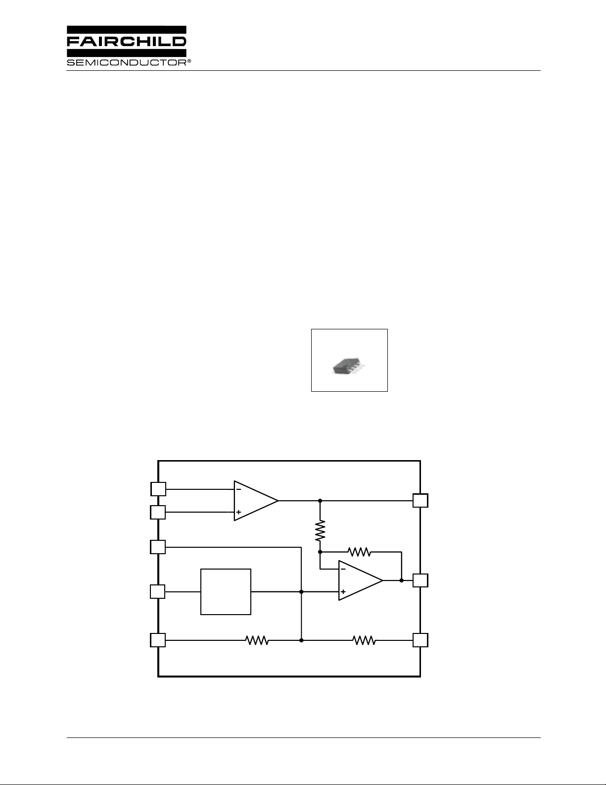
Internal Block Diagram
Description
The FAN7021 is a bridge connected audio power amplifier
capable of delivering 1W of continuous average power to an
8Ω load with less than 0.2%(THD) from a 5V power supply.
The FAN7021 require few external components and operate
on low supply voltage from 2.0V to 5.5V. Since the
FAN7021 does not require output coupling capacitor,
bootstrap capacitors, or snubber networks, it is ideally suited
for low power portable systems that requ i re minimum
volume and weight. The FAN7021 feqtures an externally
controlled, low power consumption shutdown mode (0.01
uA,typ). Additional FAN7021 features include thermal
shutdown protection, unity gain stability, and external gain
set.
8-SOP-225
1
IN-
IN+
BP
SD
VDD
©2002 Fairchild Semiconductor Corporation
4
3
2
1
6
Bias
100kΩ
20kΩ
20kΩ
100kΩ
5
8
7
O1
V
V
O2
GND
Rev. 1.0.1
Page 2
FAN7021
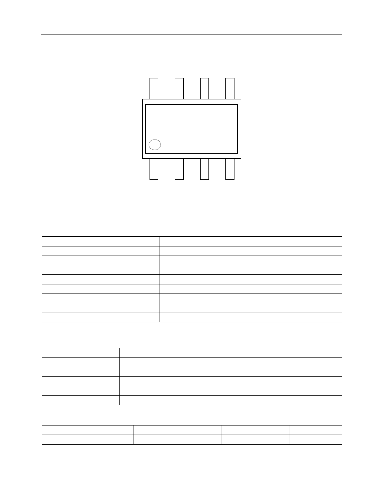
Pin Assignments
V
O2
GND V
DD
V
O1
8 7 6 5
FAN7021
1 2 3 4
SD BP IN+ IN-
Pin Definitions
Pin Number Pin Name Pin Function Description
1 SD Shutdown
2 BP Bypass
3 IN+ Input +
4IN− Input −
5V
6V
O1
DD
7 GND Ground
8V
O2
Power AMP Output 1
Supply Voltage
Power AMP Output 2
Absolute Maximum Ratings (Ta = 25°°°°C)
Parameter Symbol Value Unit Remark
Maximum Supply Voltage V
Power Dissipation P
Operating Temperature T
Storage Temperature T
Thermal Resistance θ
DD
D
OPR
STG
JA
6.0 V Maximum Supply Voltage
-W -
−40 ~ +85 °C Operating Temperature
−65 ~ +150 °C Storage Temperature
180 °C/W Thermal Resistance
Recommended Operating Conditions (Ta = 25°°°°C)
Parameter Symbol Min. Typ. Max. Unit
Operating Supply Voltage V
2
DD
2.0 - 5.5 V
Page 3
FAN7021
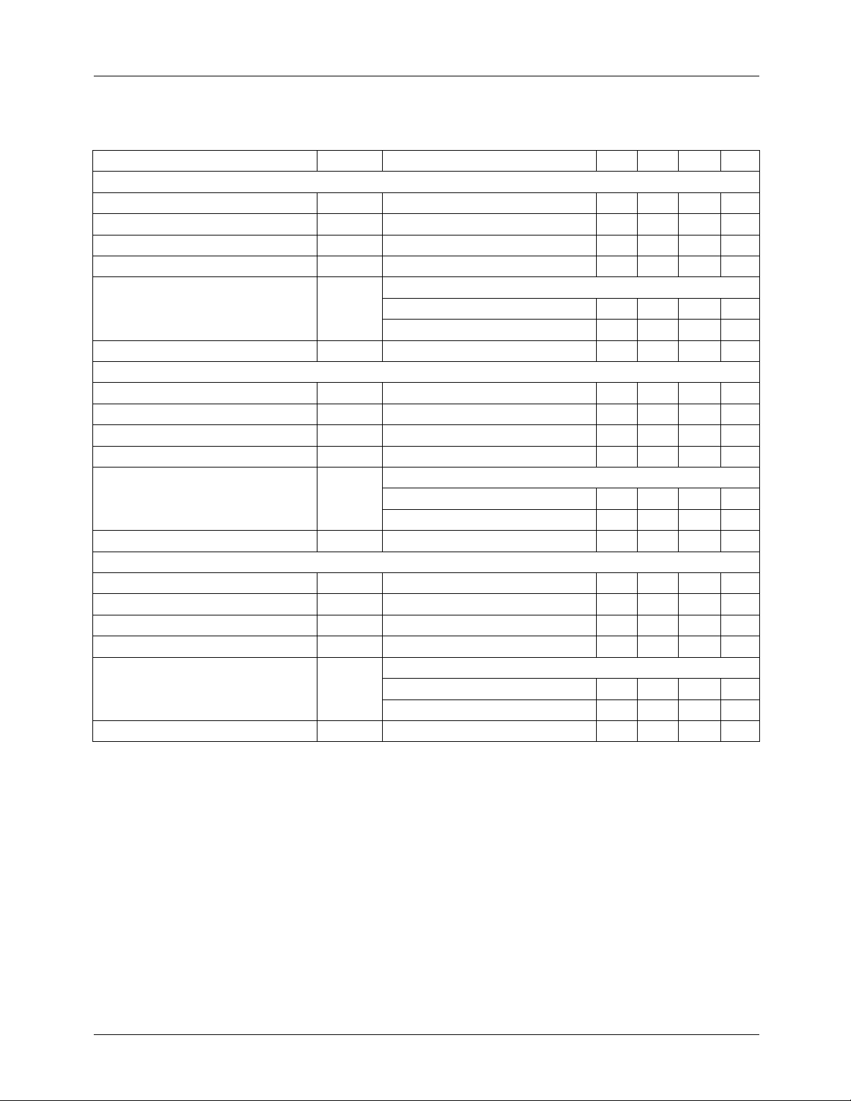
Electrical Characteristics
(RL = 8Ω
, Ta = 25°C,
Parameter Symbol Conditions Min. Typ. Max. Unit
V
= 5.0V, UNLESS OTHERWISE SPECIFIED
DD
Quiescent Power Supply Current I
Shutdown Current I
Output Offset Voltage V
Output Power P
Total Harmonic Distortion+noise THD+N
Power Supply Rejection Ratio PSRR V
= 3.3V, UNLESS OTHERWISE SPECIFIED
V
DD
Quiescent Power Supply Current I
Shutdown Current I
Output Offset Voltage V
Output Power P
Total Harmonic Distortion+noise THD+N
Power Supply Rejection Ratio PSRR V
= 2.6V, UNLESS OTHERWISE SPECIFIED
V
DD
Quiescent Power Supply Current I
Shutdown Current I
Output Offset Voltage V
Output Power P
Total Harmonic Distortion+Noise THD+N
Power Supply Rejection Ratio PSRR V
Unless otherwise specified)
DD
SD
OS
O
DD
SD
OS
O
DD
SD
OS
O
VIN=0V,IO=0A - 4.0 7.0 mA
VSD=V
DD
- 0.01 2.0 µA
VIN=0V - 5 50 mV
THD=0.2% (Max.);f=1KHz - 1 - W
=0.25Wrms,AVD=2
P
O
f=1KHz - 0.1 - %
f=20KHz - 0.4 - %
=4.9V to 5.1V - 65 - dB
DD
VIN=0V,IO=0A - 3.0 - mA
VSD=V
DD
-0.01- µA
VIN=0V - 5 - mV
THD=1% (Max.);f=1KHz - 0.5 - W
=0.25Wrms,AVD=2
P
O
f=1KHz - 0.15 - %
f=20KHz - 0.45 - %
=3.2V to 3.4V - 65 - dB
DD
VIN=0V,IO=0A - 2.5 - mA
VSD=V
DD
-0.01- µA
VIN=0V - 5 - mV
THD=0.3% (Max.);f=1KHz - 0.25 - W
=0.25Wrms,AVD=2
P
O
f=1KHz - 0.25 - %
f=20KHz - 0.5 - %
=2.5V to 2.7V - 65 - dB
DD
3
Page 4
FAN7021
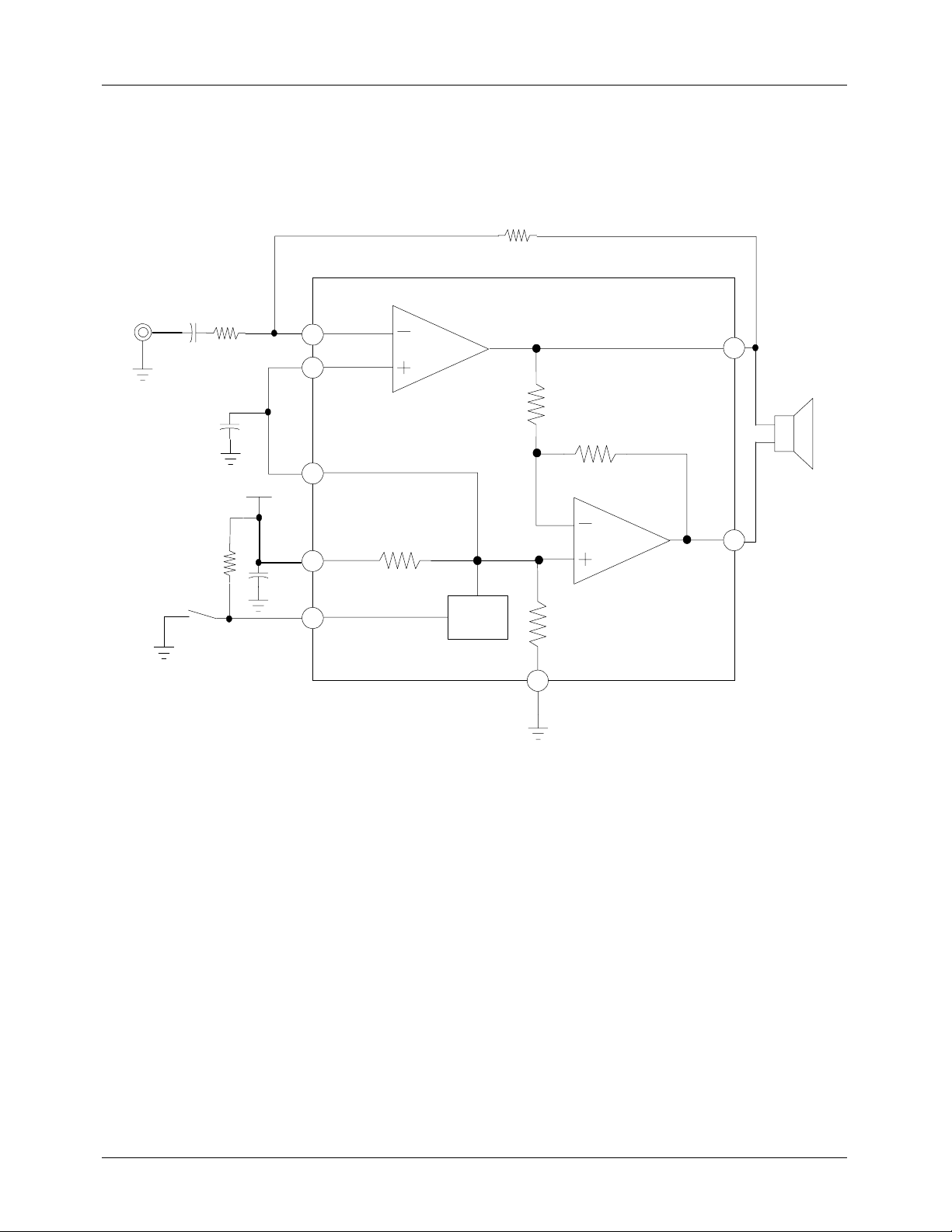
Typical Application Circuits
C
I
0.47uF
+
C
1uF
R
10KΩ
R
I
20KΩ
B
PU
+
V
DD
+
C
10uF
IN-
4
3
IN+
BP
2
V
DD
6
S
1
SD
100K
R
F
20KΩ
5
V
O1
20KΩ
20K
Ω
Speaker
8Ω
V
Ω
Bias
100KΩ
O2
8
7
GND
4
Page 5
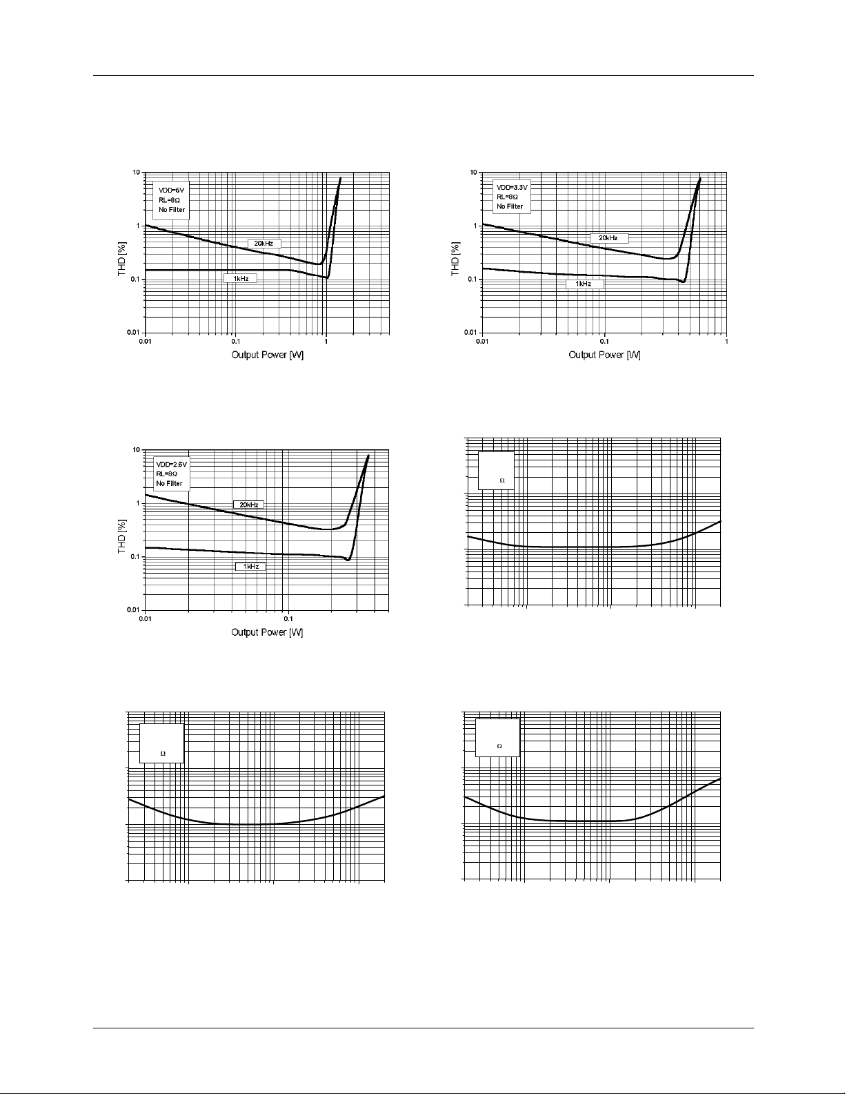
Performance Characteri stics
FAN7021
Figure 1. THD+N versus output power
Figure 3. THD+N versus output power
10
VDD=3.3V
Po=250mW
RL=8
1
Figure 2. THD+N versus output power
Frequency [Hz]
0.01
10
VDD=5V
Po=1W
RL=8
1
THD [%]
0.1
100 1k 10k
Figure 4. THD+N versus Frequency
10
VDD=2.6V
Po=250mW
RL=8
1
THD [%]
0.1
0.01
100 1k 10k
Frequency [Hz]
Figure 5. THD+N versus Frequency
0.01
THD [%]
0.1
1001k10k
Frequency [Hz]
Figure 6. THD+N versus Frequency
5
Page 6
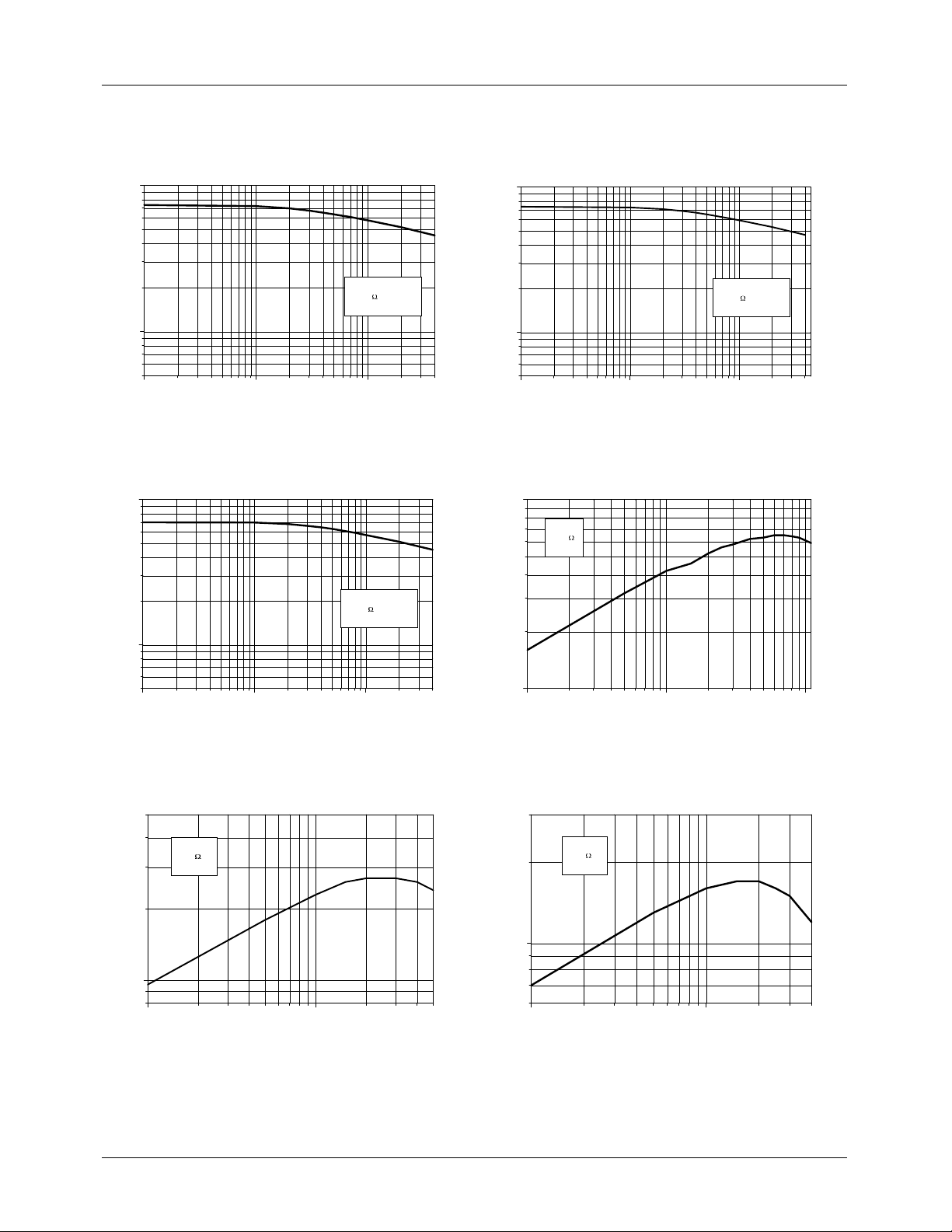
FAN7021
VDD=5V
RL=8
V
=250mVrms
ripple
(Continued)
Performance Characteristics
100
PSRR [dB]
10
1001k10k
Frequency [Hz]
100
100
PSRR [dB]
10
100 1k 10k
VDD=3.3V
RL=8
V
=250mVrms
ripple
Frequency [Hz]
Figure 8. Power supply rejection rationFigure 7. Power supply rejection ration
1
VDD=5V
RL=8
f=1kHz
VDD=2.6V
PSRR [dB]
10
100 1k 10k
RL=8
V
ripple
Frequency [Hz]
Figure 9. Power supply rejection ration
VDD=3.3V
RL=8
f=1kHz
Power Dissipation [W]
0.1
10 100
Output Power [mW]
=150mVrms
Power Dissipation [W]
0.1
10 100 1000
Output Power [mW]
Figure 10. Power Dissipation versus output power
VDD=2.6V
RL=8
f=1kHz
0.1
Power Dissipation [W]
10 100
Output Power [mW]
Figure 11. Power Dissipation versus output power Figure 12. Power Dissipation versus output power
6
Page 7
FAN7021
Performance Characteristics
(Continued)
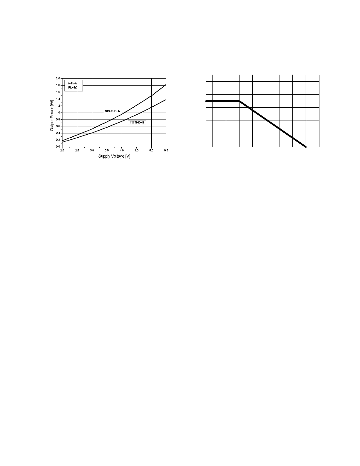
Figure 13. Output power versus supply voltage
1
0.8
0.6
0.4
0.2
Power Dissipation [W]
25
Ambient Temperature [oC]
Figure 14. Power darting curve
85-40
150
7
Page 8
FAN7021
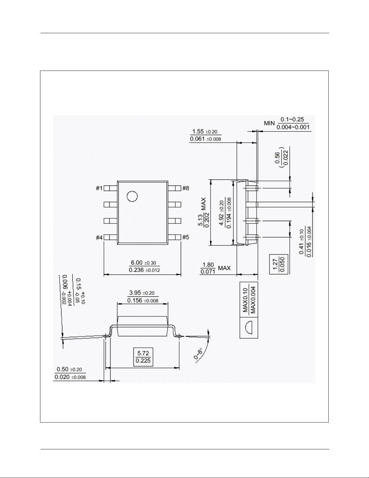
Mechanical Dimensions (Unit: mm)
Package
8-SOP-225
8
Page 9

Ordering Information
Device Package Operating Temp.
FAN7021M 8-SOP-225 −40°C ~ +85°C
FAN7021
9
Page 10

FAN7021
DISCLAIMER
FAIRCHILD SEMICONDUCTOR RESERVES THE RIGHT TO MAKE CHANGES WITHOUT FURT HER NOTICE TO ANY
PRODUCTS HEREI N TO IMPROVE RELIABILITY, FUNCTIO N OR DESIGN. FAIRCH IL D DOES NOT ASSUME ANY
LIABILITY ARISING OUT OF THE APPLICATION OR USE OF ANY PRODUCT OR CIRCUIT DESCRIBED HEREIN; NEITHER
DOES IT CONVEY ANY LICENSE UNDER IT S PATENT RIGHTS, NOR THE RIGHTS OF OTHE RS.
LIFE SUPPORT POL I CY
FAIRCHILD’S PR ODUCTS ARE NOT AUTH ORIZED FOR USE AS C RITICAL COMPONENT S IN LIFE SUPPORT DE VICES
OR SYSTEMS WITHOUT THE EXPRESS WRITTEN APPROVAL OF THE PRESIDENT OF FAIRCHILD SEMICONDUCTOR
CORPORATION. As used herein :
1. Life support devices or systems are devices or systems
which, (a) are intended for surgical implant into the body,
or (b) support or sustain life, and (c) whose failure to
perform when properly used in accordance with
2. A critical component in any component of a life support
device or sy stem whose fai lure to perform can be
reasonably expec ted to cause the failur e of the life support
device or system, or to affect its safety or effec t iv ene ss .
instructions for use provided in the labeling, can be
reasonably expected to result in a significant injury of the
user.
www.fairchildsemi.com
2/18/02 0.0m 001
2002 Fairchild Semiconductor Corporation
Stock#DSxxxxxxxx
 Loading...