


AM/FM RADIO KIT
MODEL AM/FM-108CK SUPERHET RADIO
CONTAINS TWO SEPARATE AUDIO SYSTEMS:
IC AND TRANSISTOR
Assembly and Instruction Manual
ELENCO®
Copyright © 2012 by ELENCO® All rights reserved. |
753510 |
No part of this book shall be reproduced by any means; electronic, photocopying, or otherwise without written permission from the publisher.

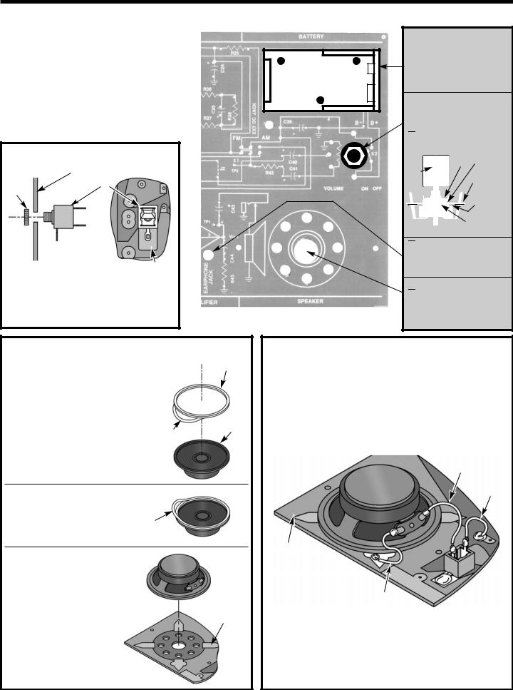
The AM/FM Radio project is divided into two parts, the AM Radio Section and the FM Radio Section. At this time, only identify the parts that you will need for the AM radio as listed below. DO NOT OPEN the bags listed for the FM radio. A separate parts list will be shown for the FM radio after you have completed the AM radio.
PARTS LIST FOR THE AM RADIO SECTION
If you are a student, and any parts are missing or damaged, please see instructor or bookstore.
If you purchased this kit from a distributor, catalog, etc., please contact ELENCO® (address/phone/e-mail is at the back of this manual) for additional assistance, if needed. DO NOT contact your place of purchase as they will not be able to help you.
RESISTORS
Qty. |
Symbol |
Value |
Color Code |
Part # |
r 1 |
R45 |
10Ω 5% 1/4W |
brown-black-black-gold |
121000 |
r 2 |
R44, 48 |
47Ω 5% 1/4W |
yellow-violet-black-gold |
124700 |
r 4 |
R38, 43, 50, 51 |
100Ω 5% 1/4W |
brown-black-brown-gold |
131000 |
r 1 |
R49 |
330Ω 5% 1/4W |
orange-orange-brown-gold |
133300 |
r 1 |
R41 |
470Ω 5% 1/4W |
yellow-violet-brown-gold |
134700 |
r 1 |
R37 |
1kΩ 5% 1/4W |
brown-black-red-gold |
141000 |
r 1 |
R42 |
2.2kΩ 5% 1/4W |
red-red-red-gold |
142200 |
r 3 |
R33, 36, 46 |
3.3kΩ 5% 1/4W |
orange-orange-red-gold |
143300 |
r 1 |
R40 |
10kΩ 5% 1/4W |
brown-black-orange-gold |
151000 |
r 1 |
R32 |
12kΩ 5% 1/4W |
brown-red-orange-gold |
151200 |
r 1 |
R35 |
27kΩ 5% 1/4W |
red-violet-orange-gold |
152700 |
r 1 |
R39 |
39kΩ 5% 1/4W |
orange-white-orange-gold |
153900 |
r 1 |
R31 |
56kΩ 5% 1/4W |
green-blue-orange-gold |
155600 |
r 1 |
R47 |
470kΩ 5% 1/4W |
yellow-violet-yellow-gold |
164700 |
r 1 |
R34 |
1MΩ 5% 1/4W |
brown-black-green-gold |
171000 |
r 1 |
Volume/S2 |
50kΩ / SW |
Potentiometer / switch with nut and plastic washer |
192522 |
CAPACITORS
Qty. |
Symbol |
Value |
Description |
Part # |
r 1 |
C30 |
150pF |
Discap (151) |
221510 |
r 1 |
C46 |
0.001μF |
Discap (102) |
244780 |
r 2 |
C31, 38 |
0.01μF |
Discap (103) |
241031 |
r 5 |
C29, 33, 35, 36, 37 |
0.02μF or 0.022μF |
Discap (203) or (223) |
242010 |
r 1 |
C44 |
0.047μF |
Discap (473) |
244780 |
r 2 |
C28, C45 |
0.1μF |
Discap (104) |
251010 |
r 4 |
C32, 40, 41, 42 |
10μF |
Electrolytic radial (Lytic) |
271045 |
r 1 |
C47 |
47μF |
Electrolytic radial (Lytic) |
274744 |
r 1 |
C34 |
100μF |
Electrolytic radial (Lytic) |
281044 |
r 2 |
C39, 43 |
470μF |
Electrolytic radial (Lytic) |
284744 |
r 1 |
C1 |
Variable |
Tuning gang AM/FM |
299904 |
SEMICONDUCTORS
Qty. |
Symbol |
Value |
Description |
Part # |
r 2 |
D4, 5 |
1N4148 |
Diode |
314148 |
r 5 Q7, 8, 9, 10, 11 |
2N3904 |
Transistor NPN |
323904 |
|
r 1 |
Q12 |
2N3906 |
Transistor PNP |
323906 |
r 1 |
Q14 |
JE8050 |
Transistor NPN |
328050 |
r 1 |
Q13 |
JE8550 |
Transistor PNP |
328550 |
r 1 |
U1 |
LM386 |
Integrated circuit |
330386 |
|
|
|
COILS |
|
|
MAGIC WAND |
|
Qty. |
Symbol |
Color |
Description |
Part # |
Qty. |
Description |
Part # |
r 1 |
L5 |
Red |
AM oscillator |
430057 |
r 1 |
Iron core |
461000 |
r 1 |
T6 |
Yellow |
AM IF |
430260 |
r 1 |
Brass core |
661150 |
r 1 |
T7 |
White |
AM IF |
430262 |
r 4” |
Shrink tubing |
890120 |
r 1 |
T8 |
Black |
AM IF |
430264 |
|
|
|
r 1 |
L4 |
|
AM antenna with holders |
484004 |
|
|
|
|
|
|
|
|
|
|
|
-1-

PARTS LIST FOR THE AM RADIO SECTION (continued)
MISCELLANEOUS
Qty. |
Description |
Part # |
r 1 |
PC board, transistor audio amplifier |
510007 |
r 1 |
PC board, main |
517055 |
r 1 |
Switch |
541023 |
r 1 |
Battery holder |
590096 |
r 1 |
Speaker |
590102 |
r 2 |
Header male 4-pin |
591004 |
r 1 |
Speaker pad |
780128 |
r 1 |
Knob (dial) |
622040 |
r 1 |
Knob (pot) |
622050 |
r 1 |
Earphone jack with nut |
622130 |
r 1 |
Radio stand |
626100 |
Qty. |
Description |
Part # |
r 1 |
Earphone |
629250 |
r 3 |
Screw M1.8 x 7.5mm (battery holder) |
641100 |
r 1 |
Screw M2.5 x 7.5mm (dial) |
641107 |
r 2 |
Screw M2.5 x 3.8mm (gang) |
641310 |
r 3 |
Nut M1.8 |
644210 |
r 1 |
Plastic washer |
645108 |
r 1 |
Socket 8-pin |
664008 |
r 12 |
Test point pin |
665008 |
r 1 |
Label AM/FM |
723059 |
r 8” |
Wire 22AWG insulated |
814520 |
r 1 |
Solder lead-free |
9LF99 |
Note: The following parts are used in the Transistor Audio Amplifier Section (packaged in a separate bag) – R46, R47, R48, R49, R50, R51, C46, C47, D5, Q10, Q11, Q12, Q13, Q14, PC board (transistor audio amplifier), test point pin (qty. 4), and header male 4-pin (qty. 2).
**** SAVE THE BOX THAT THIS KIT CAME IN. IT WILL BE USED ON PAGES 32 & 61. ****
PARTS IDENTIFICATION
|
RESISTORS |
|
|
MISCELLANEOUS |
|
|
50kΩ Potentiometer / switch |
Knob (dial) |
|
|
|
||
|
with nut, metal washer, |
|
|
|
||
|
|
|
|
|
||
|
and plastic washer |
|
|
|
|
|
|
CAPACITORS |
|
Knob |
|
|
|
|
|
|
(pot) |
|
|
|
|
|
|
|
Label AM/FM |
Earphone |
|
|
|
|
|
|
Shrink tubing |
|
Discap |
|
Tuning gang |
|
|
|
|
|
Electrolytic radial |
AM/FM |
|
Brass core |
Iron core |
|
|
|
|
|
|||
|
SEMICONDUCTORS |
|
|
Test point pin |
|
|
|
|
|
|
|
Earphone jack |
|
|
|
|
|
|
|
|
|
|
|
|
|
|
with nut |
|
Diode |
|
Speaker |
|
|
|
|
|
|
|
|
|
|
|
|
|
|
Slide switch |
|
|
Transistor |
LM386 IC |
|
|
Speaker pad |
8-pin Socket |
|
|
COILS |
|
|
|
|
|
Color dot |
|
|
|
|
|
|
|
Ferrite core |
|
|
|
|
|
|
Coil |
Plastic holders |
Battery holder |
Header male 4-pin |
|
|
|
|
|
||||
|
|
|
Screw |
|
Nut |
|
|
|
|
M2.5 x 3.8mm |
|
M1.8 |
|
|
|
|
Screw M1.8 x 7.5mm |
Screw M2.5 x 7.5mm |
|
|
Coil |
Antenna Assembly |
Hardware |
Radio stand |
|||
|
|
|
-2- |
|
|
|

IDENTIFYING RESISTOR VALUES
Use the following information as a guide in properly identifying the value of resistors.
BAND 1 |
|
BAND 2 |
|
Multiplier |
|
Resistance |
|
|
|
|
||||
1st Digit |
|
2nd Digit |
|
|
|
|
Tolerance |
|
|
|
|
|||
Color |
Digit |
|
Color |
Digit |
|
Color |
Multiplier |
|
Color |
Tolerance |
|
|
BANDS |
|
Black |
0 |
|
Black |
0 |
|
Black |
1 |
|
Silver |
±10% |
|
|
|
|
Brown |
1 |
|
Brown |
1 |
|
Brown |
10 |
|
Gold |
±5% |
1 |
2 |
Multiplier |
Tolerance |
Red |
2 |
|
Red |
2 |
|
Red |
100 |
|
Brown |
±1% |
|
|
|
|
Orange |
3 |
|
Orange |
3 |
|
Orange |
1,000 |
|
Red |
±2% |
|
|
|
|
Yellow |
4 |
|
Yellow |
4 |
|
Yellow |
10,000 |
|
Orange |
±3% |
|
|
|
|
Green |
5 |
|
Green |
5 |
|
Green |
100,000 |
|
Green |
±0.5% |
|
|
|
|
Blue |
6 |
|
Blue |
6 |
|
Blue |
1,000,000 |
|
Blue |
±0.25% |
|
|
|
|
Violet |
7 |
|
Violet |
7 |
|
Silver |
0.01 |
|
Violet |
±0.1% |
|
|
|
|
Gray |
8 |
|
Gray |
8 |
|
Gold |
0.1 |
|
|
|
|
|
|
|
|
|
|
|
|
|
|
|
|
||||||
White |
9 |
|
White |
9 |
|
|
|
|
|
|
|
|
|
|
IDENTIFYING CAPACITOR VALUES
Capacitors will be identified by their capacitance value in pF (picofarads), nF (nanofarads), or μF (microfarads). Most capacitors will have their actual value printed on them. Some capacitors may have their value printed in the following manner. The maximum operating voltage may also be printed on the capacitor.
Electrolytic capacitors have a positive and a negative electrode. The negative lead is indicated on the packaging by a stripe with minus signs and possibly arrowheads. Also, the negative lead of a radial electrolytic is shorter than the positive one.
Multiplier |
For the No. |
|
0 |
1 |
2 |
3 |
4 |
5 |
8 |
9 |
|||
|
|
|
|
|
|
|
|
|
|
|
|
|
|
Multiply By |
|
1 |
10 |
100 |
1k |
10k |
100k |
.01 |
0.1 |
||||
|
|
||||||||||||
|
|
|
|
|
|
|
|
|
|
|
|
|
|
Second Digit |
|
|
|
|
Multiplier |
|
|
|
|
|
|
||
103K |
|
|
|
|
|
|
|||||||
First Digit |
Tolerance* |
|
|
|
|
|
|||||||
100V |
|
|
|
|
|
||||||||
Warning:
If the capacitor is connected with incorrect polarity, it may heat up and either leak, or cause the capacitor to explode.
(+) (–)
Axial
Polarity marking
(–)
(+)
Radial
Maximum Working Voltage
The value is 10 x 1,000 = 10,000pF or .01μF 100V
*The letter M indicates a tolerance of +20% |
Note: The letter “R” |
may be used at times |
|
The letter K indicates a tolerance of +10% |
to signify a decimal |
The letter J indicates a tolerance of +5% |
point; as in 3R3 = 3.3 |
METRIC UNITS AND CONVERSIONS
Abbreviation |
Means |
Multiply Unit By |
Or |
|
1. |
1,000 pico units |
= 1 nano unit |
p |
Pico |
.000000000001 |
10-12 |
|
2. |
1,000 nano units |
= 1 micro unit |
n |
nano |
.000000001 |
10-9 |
|
|||
|
3. |
1,000 micro units |
= 1 milli unit |
||||
μ |
micro |
.000001 |
10-6 |
|
|||
m |
milli |
.001 |
10-3 |
|
4. |
1,000 milli units |
= 1 unit |
– |
unit |
1 |
100 |
|
5. |
1,000 units |
= 1 kilo unit |
k |
kilo |
1,000 |
103 |
|
|||
|
6. |
1,000 kilo units |
= 1 mega unit |
||||
M |
mega |
1,000,000 |
106 |
|
|||
|
|
|
|
|
|
|
|
-3-

INTRODUCTION
The Elenco® Superhet 108C AM/FM Radio Kit is a “superheterodyne” receiver of the standard AM (amplitude modulation) and FM (frequency modulation) broadcast frequencies. The unique design of the Superhet 108 allows you to place the parts over their corresponding symbol in the schematic drawing on the surface of the printed circuit board during assembly. This technique maximizes the learning process while keeping the chances of an assembly error at a minimum. It is very important, however, that good soldering practices are used to prevent bad connections. The Soldering Guide should be reviewed before any soldering is attempted.
The actual assembly is broken down into 9 sections. The theory of operation for each section, or stage, should be read before the assembly is started. This will provide the student
with an understanding of what that stage has been designed to accomplish, and how it actually works. After each assembly, you will be instructed to make certain tests and measurements to prove that each section is functioning properly. If a test fails to produce the proper results, a troubleshooting guide is provided to help you correct the problem. If test equipment is available, further measurements and calculations are demonstrated to allow each student to verify that each stage meets the engineering specifications. After all of the stages have been built and tested, a final alignment procedure is provided to peak the performance of the receiver and maximize the Superhet 108’s reception capabilities.
GENERAL DISCUSSION
|
|
|
|
FM RADIO |
|
|
Section 9 |
|
Section 8 |
Section 7 |
Section 6 |
|
|
FM RF |
FM MIXER |
|
|
|
Figure 1 |
|
AMPLIFIER |
|
|
|
|
||
|
|
|
|
|
|
|
|
|
|
1ST FM IF |
2ND FM IF |
FM |
|
|
|
|
AMPLIFIER |
AMPLIFIER |
DETECTOR |
|
FM |
|
AFC |
|
|
|
Speaker |
OSCILLATOR |
|
|
|
|
IC or |
|
|
|
|
|
|
||
|
|
|
|
|
|
TRANSISTOR |
|
|
|
|
|
|
AUDIO |
|
|
|
|
|
|
AMPLIFIER |
AM MIXER |
|
1ST AM IF |
2ND AM IF |
AM |
|
|
|
AMPLIFIER |
AMPLIFIER |
DETECTOR |
|
||
|
|
|
|
|||
AM |
|
|
|
|
AGC |
|
OSCILLATOR |
|
|
|
|
||
|
|
|
|
|
||
Section 5 |
|
Section 4 |
Section 3 |
Section 2 |
Section 1 |
|
|
|
|
|
AM RADIO |
|
|
The purpose of Section 1, the Audio Amplifier Stage, is to increase the power of the audio signal received from either detector to a power level capable of driving the speaker. The audio amplifier is IC or transistor version. Section 2 includes the AM detector circuit and the AGC (automatic gain control) stage. The AM detector converts the amplitude modulated IF (intermediate frequency) signal to a low level audio signal. The AGC stage feeds back a DC voltage to the first AM IF amplifier in order to maintain a near constant level of audio at the detector. Section 3 is the second AM IF amplifier. The second AM IF amplifier is tuned to 455kHz (Kilohertz) and has a fixed gain at this frequency of 50. Section 4 is the first AM IF 2 amplifier which has a variable gain that depends on the AGC voltage received from the AGC stage. The first AM IF amplifier is also tuned to 455kHz. Section 5 includes the AM mixer, AM oscillator and AM antenna stages. When the radio wave passes through the antenna, it induces a small voltage across the antenna coil. This voltage is coupled to the mixer, or converter, stage to be changed to a frequency of 455kHz. This change is accomplished by mixing (heterodyning) the radio frequency signal with the oscillator
signal. Section 6 is the FM ratio detector circuit. The FM ratio detector has a fixed gain of about 20. Section 7 is the second FM IF amplifier. The second FM IF amplifier is tuned to 10.7MHz (Megahertz) and has a set gain of approximately 20. The 3dB bandwidth of this stage should be approximately 350kHz. Section 8 is the first FM IF amplifier. The first FM IF amplifier is also tuned to 10.7MHz and has a set gain of approximately 10. It also has a 3dB bandwidth of 350kHz. Section 9 includes the FM mixer, FM oscillator, FM RF (Radio Frequency) amplifier, AFC (Automatic Frequency Control) stage, and the FM antenna. The incoming radio waves are amplified by the FM RF amplifier, which is tuned to a desired radio station in the FM frequency bandwidth of 88MHz to 108MHz. These amplified signals are then coupled to the FM mixer stage to be changed to a frequency of 10.7MHz. This change, as in AM, is accomplished by heterodyning the radio frequency signal with the oscillator signal. The AFC stage feeds back a DC voltage to the FM oscillator to prevent the oscillator from drifting. Each of these blocks will be explained in detail in the Theory of Operation given before the assembly instructions for that stage.
-4-

CONSTRUCTION
Introduction
The most important factor in assembling your Superhet 108C AM/FM Radio Kit is good soldering techniques. Using the proper soldering iron is of prime importance. A small pencil type soldering iron of 25 watts is recommended. The tip of the iron must be kept clean at all times and well tinned.
Solder
For many years leaded solder was the most common type of solder used by the electronics industry, but it is now being replaced by leadfree solder for health reasons. This kit contains lead-free solder, which contains 99.3% tin, 0.7% copper, and has a rosin-flux core.
Lead-free solder is different from lead solder: It has a higher melting point than lead solder, so you need higher temperature for the solder to flow properly. Recommended tip temperature is approximately 700OF; higher temperatures improve solder flow but accelerate tip decay. An increase in soldering time may be required to achieve good results. Soldering iron tips wear out faster since lead-free solders are more corrosive and the higher soldering temperatures accelerate corrosion, so proper tip care is important. The solder joint finish will look slightly duller with lead-free solders.
Use these procedures to increase the life of your soldering iron tip when using lead-free solder:
•Keep the iron tinned at all times.
•Use the correct tip size for best heat transfer. The conical tip is the most commonly used.
•Turn off iron when not in use or reduce temperature setting when using a soldering station.
•Tips should be cleaned frequently to remove oxidation before it becomes impossible to remove. Use Dry Tip Cleaner (Elenco® #SH-1025) or Tip Cleaner (Elenco® #TTC1). If you use a sponge to clean your tip, then use distilled water (tap water has impurities that accelerate corrosion).
Safety Procedures
•Always wear safety glasses or safety goggles to ' protect your eyes when working with tools or soldering iron, and during all phases of testing.
•Be sure there is adequate ventilation when soldering.
•Locate soldering iron in an area where you do not have to go around it or reach over it. Keep it in a safe area away from the reach of children.
•Do not hold solder in your mouth. Solder is a toxic substance. Wash hands thoroughly after handling solder.
Assemble Components
In all of the following assembly steps, the components must be installed on the top side of the PC board unless otherwise indicated. The top legend shows where each component goes. The leads pass through the corresponding holes in the board and are soldered on the foil side.
Use only rosin core solder.
DO NOT USE ACID CORE SOLDER!
What Good Soldering Looks Like
A good solder connection should be bright, shiny, smooth, and uniformly flowed over all surfaces.
|
|
|
|
Soldering Iron |
|
|
|
|
|
|
|
1. Solder all components from the |
Component Lead |
||||
|
|
|
|
|
|
|
|
|
|
|
|
copper foil side only. Push the |
|
Foil |
|
||
soldering iron tip against both the |
|
|
|
|
|
lead and the circuit board foil. |
|
|
|
|
|
Circuit Board
2.Apply a small amount of solder to the iron tip. This allows the heat to leave the iron and onto the foil. Immediately apply solder to the opposite side of the connection, away from the iron. Allow the heated component and the circuit foil to melt the solder.
Soldering Iron
Solder
Foil
|
|
|
|
|
|
|
|
|
|
3. Allow the solder to flow around |
|
|
Solder |
Soldering Iron |
|
||||
|
|
|
|
||||||
|
|
|
|
|
|
|
|||
the connection. |
Then, |
remove |
|
|
|
Foil |
|
|
|
the solder and the iron and let the |
|
|
|
|
|
|
|||
|
|
|
|
|
|
|
|||
connection cool. |
The |
solder |
|
|
|
|
|
|
|
should have flowed smoothly and |
|
|
|
|
|
|
|
||
not lump around the wire lead. |
|
|
|
|
|
|
|
||
|
|
|
|
|
|
|
|
|
|
|
|
|
|
|
|
|
|
|
|
4.Here is what a good solder connection looks like.
Types of Poor Soldering Connections
Rosin
1. Insufficient heat - the solder will not flow onto the lead as shown.
Soldering iron positioned incorrectly.
2.Insufficient solder - let the solder flow over the connection until it is covered.
Use just enough solder to cover the connection.
3.Excessive solder - could make connections that you did not intend to between adjacent foil areas or terminals.
Solder
Gap
Component Lead
Solder
4.Solder bridges - occur when solder runs between circuit paths and creates a short circuit. This is usually caused by using too much solder.
To correct this, simply drag your soldering iron across the solder bridge as shown.
|
Soldering Iron |
Foil |
Drag |
-5-

SEMICONDUCTOR PARTS FAMILIARIZATION
This section will familiarize you with the proper method used to test the transistors and the diode.
TRANSISTOR TEST (NPN and PNP)
Refer to the parts list and find a NPN transistor. Refer the Figure J (page 16) for locating the Emitter, Base and Collector. Using an Ohmmeter, connect the transistor as shown in Test A. Your meter should be reading a low resistance. Switch the lead from the Emitter to the Collector. Your meter should again be reading a low resistance.
Using an Ohmmeter, connect the transistor as shown in Test B. Your meter should be reading a high resistance. Switch the lead from the Emitter to the Collector. Your meter should again be reading a high resistance. Typical results read approximately 1MΩ to infinity.
Refer to parts list and find a PNP transistor, refer to Figure K (page 16) for locating the Emitter, Base and Collector. Using an Ohmmeter, connect the transistor as shown in Test C. Your meter should be reading a low resistance. Switch the lead from the Emitter to the Collector. Your meter should again be reading a low resistance.
Using an Ohmmeter, connect the transistor as shown in Test D. Your meter should be reading a high resistance. Switch the lead from the Emitter to the Collector. Your meter should again be reading a high resistance.
|
|
|
|
|
|
|
|
|
|
|
|
|
|
|
|
|
|
Low Resistance |
|
|
|
High Resistance |
|
|
|
Low Resistance |
|
|
|
High Resistance |
|
|
Ω |
|
|
|
Ω |
|
|
|
Ω |
|
|
|
Ω |
|
|
|
|
|
|
|
|
|
|
|
|
|
|
|
|
||
|
COM Ω |
NPN |
|
|
COM Ω |
NPN |
|
|
COM Ω |
PNP |
|
|
COM Ω |
PNP |
|
|
|
EBC |
|
|
|
EBC |
|
|
|
EBC |
|
|
|
EBC |
|
|
|
|
|
|
|
|
|
|
|
|
|
|
|||
|
|
|
|
|
|
|
|
|
|
|
|
|
|
|
|
|
|
|
|
|
|
|
|
|
|
|
|
|
|
|
|
|
|
|
|
|
|
|
|
|
|
|
|
|
|||
|
TEST A |
TEST B |
|
|
|
TEST C |
TEST D |
||||||||
|
|
|
|
|
|
|
|
|
|
|
|
|
|
|
|
DIODE TEST
Refer to the parts list and find a diode. Refer to Figure H (page 16) for locating the Cathode and Anode. The end with the band is the cathode. Using an Ohmmeter, connect the diode as shown in Test E. Your meter should be reading a low resistance. Using an Ohmmeter,
connect the diode as shown in Test F. Your meter should be reading a high resistance. Typical results read approximately 1MΩ to infinity for silicon diodes (1N4148).
|
|
|
|
|
|
|
|
|
|
|
|
Low Resistance |
|
|
|
|
Ω |
High Resistance |
|
|
Ω |
|
|
|
|
|
|
|
|
|
|
|
|
|
|
|
|
|
|
|
COM Ω |
|
|
|
|
COM |
Ω |
||
|
|
|
|
|
|
|
|
|
|
|
|
Diode |
|
|
|
|
Diode |
||
|
|
|
|
|
|
|
|
|
|
|
|
|
|
|
|
|
|
|
|
|
|
|
|
|
|
|
|
|
|
|
|
TEST E |
|
|
TEST F |
||||
|
|
|
|
|
|
|
|
|
|
-6-

SECTION 1A |
|
|
|
|||
INTEGRATED CIRCUIT (IC) AUDIO AMPLIFIER |
|
|
|
|
||
This radio kit contains two separate audio |
Equivalent Schematic and Connection Diagrams |
|||||
systems. The first is an integrated circuit (IC) and |
||||||
|
|
|
|
VS |
||
the second is a five-transistor circuit. The objective |
|
|
|
|
||
|
15kΩ |
|
|
6 |
||
is to show you how these two circuits function and |
|
|
|
|
||
|
7 |
|
|
|
||
to compare the performance of each. We will |
|
BYPASS |
|
|
|
|
|
|
|
|
|
||
begin the radio project by building the IC audio |
|
15kΩ GAIN |
GAIN |
|
||
amplifier first. |
|
8 |
|
1 |
|
|
|
|
|
15kΩ |
5 |
||
|
|
|
|
|||
The purpose of the Audio Amplifier is to increase |
|
|
|
|
VOUT |
|
|
150Ω |
1.35kΩ |
|
|||
the audio power to a level sufficient to drive an 8 |
|
2 |
|
3 |
|
|
ohm speaker. To do this, DC (direct current) from |
– INPUT |
|
+ INPUT |
|
||
|
|
|
|
|
||
the battery is converted by the amplifier to an AC |
|
|
|
50kΩ |
|
|
(alternating current) in the speaker. The ratio of |
|
50kΩ |
|
|
||
|
|
|
|
|||
|
|
|
|
|
||
the power delivered to the speaker and the power |
|
|
|
|
4 |
|
taken from the battery is the efficiency of the |
|
|
|
|
||
|
|
|
|
GND |
||
amplifier. For the Audio Amplifier, we use the |
Dual-In-Line and Small |
|
|
|
||
integrated circuit (IC) LM-386. In Figure 2, you can |
|
|
|
|||
Outline Packages |
|
|
|
|||
see equivalent schematic and connection |
|
|
|
|||
|
|
|
|
|
||
diagrams. |
1 |
8 |
|
|
|
|
|
GAIN |
GAIN |
|
|
|
|
In a Class A amplifier (transistor on over entire |
2 |
7 |
|
|
|
|
cycle), the maximum theoretical efficiency is 0.5 |
– INPUT |
BYPASS |
|
|
|
|
|
|
|
|
|
||
or 50%. But, in a Class B amplifier (transistor on |
+ INPUT |
VS |
|
|
|
|
|
3 |
6 |
|
|
|
|
for 1/2 cycle), the maximum theoretical efficiency |
4 |
5 |
|
|
|
|
is 0.785 or 78.5%. Since transistor characteristics |
|
|
|
|||
GND |
VOUT |
|
|
|
||
are not ideal in a pure Class B amplifier, the |
|
Top View |
|
|
|
|
transistors will introduce crossover distortion. This |
|
|
|
|
||
|
Figure 2 |
|
Figure 3 |
|
||
is due to the non-linear transfer curve near zero |
|
|
|
|||
current or cutoff. This type of distortion is shown in |
|
|
|
|
|
|
Figure 3. |
|
gain will go up to 200 (see Figure 4b) if a capacitor is |
||||
|
|
|||||
In order to eliminate crossover distortion and maximize |
placed between pins 1 and 8. The gain can be set to any |
|||||
efficiency, the transistors of the audio amplifier circuit are |
value from 20 to 200 if a resistor is placed in series with the |
|||||
biased on for slightly more than 1/2 of the cycle, Class AB. |
capacitor. The amplifier with a gain of 150 is shown in |
|||||
In other words, the transistors are working as Class A |
Figure 4c. |
|
|
|
||
amplifiers for very small levels of power to the speaker, but |
The amplifier in our kit with a gain of 150 is shown in |
|||||
they slide toward Class B operation at larger power levels. |
||||||
Figure 5. Capacitor C40 couples the audio signal from the |
||||||
|
|
|||||
To make the LM-386 a more versatile amplifier, two pins (1 |
volume control to the input of the audio amplifier. |
|||||
and 8) are provided for gain control. With pins 1 and 8 open, |
Capacitor C43 blocks the DC to the speaker, while |
|||||
the 1.35kΩ resistor sets the gain at 20 (see Figure 4a). The |
allowing the AC to pass. |
|
||||
Typical Applications |
|
|
|
|
|
|
|
|
|
|
|
||||
|
|
|
|
|
|
|
|
|
|
|
|||||
|
|
Amplifier with Gain = 20 |
|
|
|
|
|
Amplifier with Gain = 200 |
|
|
|||||
|
|
Minimum Parts |
|
|
|
|
|
|
VS |
10μF |
|
|
|||
|
|
|
VS |
|
|
|
|
|
|
|
|
+ |
|
|
|
|
|
|
|
|
|
|
|
|
|
6 |
|
|
|
|
|
|
|
2 |
6 |
|
|
|
|
|
|
2 |
|
|
|
|
|
|
|
|
|
|
|
|
|
– |
1 |
|
|
|
|||
|
|
– |
1 |
|
|
|
|
|
|
|
|
|
|||
|
|
|
|
|
|
|
|
|
|
|
|
||||
|
|
|
|
|
|
|
|
|
|
|
|
|
|
||
|
|
|
LM386 8 + |
|
|
|
|
|
|
LM386 |
8 + |
|
|
||
VIN |
|
|
|
|
|
|
VIN |
|
5 |
|
|
||||
|
|
|
5 |
|
|
|
|
|
3 + |
|
7 |
|
|
||
|
|
3 |
|
7 |
|
|
|
|
|
|
|
|
|||
|
|
+ |
|
|
|
|
10kΩ |
|
.05μF |
|
|
||||
10kΩ |
|
.05μF |
|
|
|
|
4 |
|
|
|
|||||
|
4 |
|
|
|
|
|
|
|
|
|
|
|
|||
|
|
|
|
|
|
|
|
|
|
|
BYPASS |
|
|
||
|
|
|
|
|
|
|
|
|
|
|
|
|
|
||
|
|
|
|
10Ω |
|
|
|
|
|
|
|
|
10Ω |
|
|
|
|
|
|
|
|
|
|
|
|
|
|
|
|
|
|
Figure 4a |
|
|
|
|
|
Figure 4b |
|
|
|
|
|||||
|
|
|
|
|
|
|
|
|
|
|
|
|
|||
|
|
|
|
|
|
|
|
|
|
Amplifier with Gain = 150 |
|
|
|||
|
|
|
|
|
|
VS |
47Ω + |
|
|
|
|
|
|
||
|
|
|
|
|
|
|
|
|
|
|
|
|
|||
|
|
|
|
|
2 |
6 |
|
|
10μF |
|
|
|
|
|
|
|
|
|
|
|
– |
1 |
|
|
|
|
|
|
|
|
|
|
|
|
|
VIN |
|
LM386 |
8 |
+ |
|
|
|
|
|
||
|
|
|
|
|
5 |
|
|
|
|
|
|
||||
|
|
|
|
|
3 |
+ |
|
|
7 |
|
|
|
|
|
|
|
|
|
|
10kΩ |
|
|
|
10Ω |
|
|
|
|
|
||
|
|
|
|
|
4 |
|
|
|
|
|
|
|
|
||
|
|
|
|
|
|
|
|
BYPASS |
|
|
|
|
|
||
|
|
|
|
|
|
|
|
|
|
|
|
|
|
||
|
|
|
|
|
|
|
|
|
|
|
|
|
|
|
|
Figure 4c |
|
|
|
|
|
|
.05μF |
|
|
|
|
Figure 5 |
|||
|
|
|
|
|
|
|
|
|
|
|
|||||
|
|
|
|
|
|
|
|
|
|
|
|
|
|
|
|
-7-

ASSEMBLY INSTRUCTIONS
We will begin by installing resistor R43. Identify the resistor by its color and install as shown on page 4. Be careful to properly mount and solder all components. Diodes, transistors and electrolytic capacitors are polarized, be sure to follow the instructions carefully so that they are not mounted backwards. Check the box when you have completed each installation.
Wear safety goggles during all assembly stages in this manual. '
Test Point Pin |
|
Lytic Capacitor |
Integrated Circuit (IC) |
|
||||
Legend side of PC |
Be |
sure |
that |
the |
|
r Insert the IC socket into the PC board with the notch in |
||
negative (short) lead is |
|
the same direction as the marking on the top legend (blue |
||||||
board (blue side) |
Polarity |
|||||||
in |
the correct hole |
on |
side). Solder the IC socket into place. |
|
||||
|
mark |
|
||||||
|
the PC board. |
|
|
|
|
|||
|
|
|
|
(–) |
(+) |
r Insert the IC into the |
Dot |
|
|
Warning: |
|
socket with the notch or |
|
||||
|
|
|
|
|
||||
|
If the capacitor is connected with incorrect |
dot in the same direction |
|
|||||
|
as the notch on the socket. |
|
||||||
|
polarity, it may heat up and either leak, or |
|
||||||
Foil side of PC board |
cause the capacitor to explode. |
|
|
|
||||
|
|
Figure B |
|
|
|
|||
(green side) |
|
|
|
|
|
|||
Figure A |
|
Polarity |
|
|
|
Notch |
|
|
|
|
|
|
|
|
|||
|
|
mark |
|
|
|
|
|
|
+
|
|
|
|
|
|
|
|
|
|
|
– |
|
|
|
|
|
|
|
|
|
|
|
|||
|
|
|
|
|
|
|
|
|
|
|
|
|
|
|
|
|
|
|
Notch marking |
||||||
|
|
|
|
|
Foil side of |
|
|
|
|
|
|
|
|
|
|
|
|||||||||
|
|
|
|
|
PC board |
|
|
|
|
|
|
|
Figure D |
||||||||||||
|
|
|
|
|
(green side) Figure C |
|
|
|
|
|
|
|
|
||||||||||||
|
|
|
|
|
|
|
|
|
|
|
|
|
|
|
|
|
|
|
|
|
|
|
|
|
|
|
|
|
|
|
|
|
|
|
|
|
|
|
|
|
|
|
|
|
|
|
|
|
|
|
|
|
|
R43 - 100Ω Resistor |
|
|
|
|
|
|
|
|
|
|
|
|
|
|
|
|
|
|
|
C39 - 470μF Lytic |
|||
|
|
|
|
|
|
|
|
|
|
|
|
|
|
|
|
|
|
|
|
|
|||||
|
|
|
|
|
|
|
|
|
|
|
|
|
|
|
|
|
|
|
|
|
|||||
|
|
(brown-black-brown-gold) |
|
|
|
|
|
|
|
|
|
|
|
|
|
|
|
|
|
|
|
(see Figure C) |
|||
|
|
|
|
|
|
|
|
|
|
|
|
|
|
|
|
|
|
|
|
|
|
|
Mount on copper side. |
||
|
|
TP2 - Test Point Pin |
|
|
|
|
|
|
|
|
|
|
|
|
|
|
|
|
|
||||||
|
|
|
|
|
|
|
|
|
|
|
|
|
|
|
|
|
|
|
|
|
|
||||
|
|
(see Figure A) |
|
|
|
|
|
|
|
|
|
|
|
|
|
|
|
|
|
|
|
C40 - 10μF Lytic |
|||
|
|
|
|
|
|
|
|
|
|
|
|
|
|
|
|
|
|
|
|
|
|||||
|
|
|
|
|
|
|
|
|
|
|
|
|
|
|
|
|
|
|
|
|
|
|
|
|
(see Figure B) |
|
|
C42 - 10μF Lytic |
|
|
|
|
|
|
|
|
|
|
|
|
|
|
|
|
|
||||||
|
|
|
|
|
|
|
|
|
|
|
|
|
|
|
|
|
|
|
|
|
|
||||
|
|
(see Figure B) |
|
|
|
|
|
|
|
|
|
|
|
|
|
|
|
|
|
|
|
C41 - 10μF Lytic |
|||
|
|
|
|
|
|
|
|
|
|
|
|
|
|
|
|
|
|
|
|
|
|||||
|
|
|
|
|
|
|
|
|
|
|
|
|
|
|
|
|
|
|
|
|
|||||
|
|
|
|
|
|
|
|
|
|
|
|
|
|
|
|
|
|
|
|
|
|
|
|
|
(see Figure B) |
|
|
R44 - 47Ω Resistor |
|
|
|
|
|
|
|
|
|
|
|
|
|
|
|
|
|
||||||
|
|
|
|
|
|
|
|
|
|
|
|
|
|
|
|
|
|
|
|
|
|
||||
|
|
(yellow-violet-black-gold) |
|
|
|
|
|
|
|
|
|
|
|
|
|
|
|
|
|
|
|
C43 - 470μF Lytic |
|||
|
|
|
|
|
|
|
|
|
|
|
|
|
|
|
|
|
|
|
|
|
|||||
|
|
|
|
|
|
|
|
|
|
|
|
|
|
|
|
|
|
|
|
|
|
|
|
|
(see Figure B) |
|
|
U1 - IC Socket 8-pin |
|
|
|
|
|
|
|
|
|
|
|
|
|
|
|
|
|
||||||
|
|
|
|
|
|
|
|
|
|
|
|
|
|
|
|
|
|
|
|
|
|
||||
|
|
U1 - LM386 Integrated Circuit |
|
|
|
|
|
|
|
|
|
|
|
|
|
|
|
|
|
|
|
C44 - .047μF Discap (473) |
|||
|
|
|
|
|
|
|
|
|
|
|
|
|
|
|
|
|
|
|
|
|
|||||
|
|
|
|
|
|
|
|
|
|
|
|
|
|
|
|
|
|
|
|
|
|||||
|
|
(see Figure D) |
|
|
|
|
|
|
|
|
|
|
|
|
|
|
|
|
|
|
|
|
|||
|
|
|
|
|
|
|
|
|
|
|
|
|
|
|
|
|
|
|
TP1 - Test Point Pin |
||||||
|
|
|
|
|
|
|
|
|
|
|
|
|
|
|
|
|
|
|
|
|
|
|
|
|
|
|
|
|
|
|
|
|
|
|
|
|
|
|
|
|
|
|
|
|
|
|
|
|
|
|
(see Figure A) |
|
|
C45 - Solder the 0.1μF |
|
|
|
|
|
|
|
|
|
|
|
|
|
|
|
|
|
|
|
||||
|
|
|
|
|
|
|
|
|
|
|
|
|
|
||||||||||||
|
|
capacitor across pins 2 & 6 |
|
|
|
|
|
|
|
|
|
|
|
|
|
|
|
|
|
|
R45 - 10Ω Resistor |
||||
|
|
|
|
|
|
|
|
|
|
|
|
||||||||||||||
|
|
|
|
|
|
|
|
|
|
|
|
|
|
|
|
|
|
|
|
||||||
|
|
of IC U1 as shown. The |
|
|
|
|
|
|
|
|
|
|
|
(brown-black-black-gold) |
|||||||||||
|
|
capacitor |
prevents the IC |
|
|
|
|
|
|
|
|
|
|
|
|
||||||||||
|
|
|
|
|
|
|
|
|
|
|
|||||||||||||||
|
|
from oscillating. |
|
|
|
|
|
|
|
|
|
|
|
|
|||||||||||
|
|
Pin 6 |
0.1μF Capacitor |
|
|
|
|
|
|
|
|
|
|
|
|
||||||||||
|
|
|
|
|
|
|
|
|
|
|
|
|
|
|
|
|
|
|
|
|
|
|
|
|
|
|
|
|
|
|
|
|
|
|
|
J3 - Jumper Wire |
|
|
|
|
|
|
|
|
|
|
|
||||
|
|
|
|
|
|
|
|
|
|
|
|
|
|
|
|
|
|
|
|
|
|||||
|
|
|
|
|
|
|
|
|
|
|
|
|
|
|
|
|
|
|
|
|
|||||
|
|
|
|
|
|
|
|
|
|
(use a discarded lead) |
|
|
|
|
|
|
|
|
|
|
|
||||
|
|
|
|
|
|
|
|
|
|
|
|
|
|
|
|
|
|
|
|||||||
|
|
|
|
|
|
|
|
|
|
|
|
|
|
|
|
|
|
|
|
|
|
|
|
|
|
|
|
|
|
|
|
|
|
|
|
|
|
|
|
|
|
|
|
|
|
|
|
|
|
|
|
|
|
|
|
|
|
|
|
|
|
|
|
|
|
|
|
|
|
|
|
|
|
TP-15 - Test Point Pin (see Figure A) |
|||
|
|
|
Pin 2 |
|
|
|
|
|
|
|
|
|
|
|
|
|
|
|
|
||||||
|
|
|
|
|
|
|
|
|
|
|
|
|
|
|
|
|
|
|
|||||||
|
|
|
|
|
|
|
|
|
|
|
|
|
|
|
|||||||||||
|
|
|
|
|
|
|
|
|
|
|
|
|
|
|
|
|
|
|
|
|
|
|
|
|
|
-8-
ASSEMBLY INSTRUCTIONS
Figure E
Foil (green) side
|
|
Jack |
|
|
Nut |
|
|
|
|
|
|
3 |
|
|
|
|
2 |
|
|
1 |
1 |
- GND |
|
|
|
|
|||
|
2 |
- Tip |
|
|
|
3 |
- N.C. Tip |
GND pad |
|
|
|
Mount the jack with the nut from the foil (green) side of the PC board (terminal #1 on the GND pad of the PC board). Be sure to line up the tab with the pad on the foil side of the PC board. Solder terminal #1 to the pad of the PC board.

 Battery holder

 3 Screws M1.8 x 7.5

 3 Nuts M1.8
** Solder and cut off excess leads. **

 Volume/S2 (50kΩ Pot / SW) with nut & washer
 Plastic washer
 Knob (pot)
Nut |
Washer |
Knob |
Legend |
|
(blue) side |
|
of PC board |
|
Cut off |
|
locating pin |
Plastic washer
** Solder all 5 tabs to PC board **

 Earphone jack with Nut
(see Figure E)

 Speaker

 Speaker pad

 Wire #22AWG insulated (see Figures F & G)
Figure F
Step 1: If the speaker pad has |
Pad |
center and outside pieces, then |
|
remove them. Peel the backing off |
|
of one side of the speaker pad and |
|
stick the pad onto the speaker.
Speaker
Backing
Step 2: Remove the other backing from the speaker pad.
Backing
Step 3: Stick the speaker onto the solder side of the PC board.
Foil side of PC Board
(green side)
Figure G
Cut two 1” wires and one 1½” wire and strip ¼” of insulation off of both ends. Solder the wires in the locations shown.
1½” Wire
1” Wire
Foil side of
PC Board (green side)
1” Wire
-9-
STATIC MEASUREMENTS
POWER TEST
For all measurements, connect your equipment GND |
reading if necessary. If the current is greater than 20 |
||||||
to circuit GND TP15. Set your VOM (Volt-Ohm- |
milliamps, immediately turn the power off. The |
||||||
Millimeter) to read 2 amps DC. Connect the meter to |
current should be less than 10 milliamps. This is the |
||||||
the circuit as shown in Figure 6. Make sure that the |
current drawn by the battery when no input signal is |
||||||
volume control is in the OFF position (turned fully |
present (the “idle current”). Turn OFF the power. If |
||||||
counter-clockwise). While watching your VOM, turn |
your circuit fails this test, check that all of the parts |
||||||
the volume to the ON position (rotate clockwise until |
have been installed correctly, and check for shorts or |
||||||
a “click” is heard). The VOM should indicate a very |
poor solder connections. |
||||||
low current. Adjust your meter for a more accurate |
|
||||||
|
|
|
|
|
|
|
|
|
|
|
|
|
|
|
|
|
|
|
|
|
|
– |
+ |
|
|
|
|
|
|
||
|
|
|
|
|
|
||
|
|
|
|
|
|
||
|
|
|
|
|
|
– |
|
|
|
|
|
|
|
+ |
|
|
|
|
|
|
|
||
|
|
|
|
|
|
|
|
|
|
|
|
|
|
|
|
|
|
|
|
|
|
|
|
|
|
|
|
|
|
|
|
Figure 6
OUTPUT BIAS TEST
Put the battery into the holder.
GND
TP15
Figure 7
Adjust your VOM to read 9 volts and connect it as shown in Figure 7. Make sure that the battery, or a 9 volt power supply (if available), is properly connected and turn the power ON. The voltage at TP1 should be between 3 to 6 volts. If you get this reading, go on to the next test. If your circuit fails this test, turn the power OFF and check that the integrated circuit is
correctly inserted in the correct location. The notch of the IC must be in the same direction as marked on the PC board. Check that all resistor values are the correct value and not interchanged. All static tests must pass before proceeding to the Dynamic Tests or the next section.
-10-

If you do not have an audio generator, skip the following test and go directly to Section 1B.
DYNAMIC MEASUREMENTS
GAIN
Connect the VOM and audio generator to the circuit as shown in Figure 8.
Normally the AC gain is measured at a frequency of 1kHz. Your VOM however, may not be able to accurately read AC voltages at this frequency. Therefore, it is recommended that this test be performed at 400Hz. Set the audio generator at 400Hz and minimum voltage output. With the power ON, set your VOM to read an AC voltage of 1 volt at test point TP1. Increase the volume control about half way. Slowly increase the amplitude of the audio generator until your VOM reads 1 volt AC. Leave the audio generator at this setting and move the positive
lead of your VOM to the Jumper J3. Record the AC input voltage to the amplifier here:
Vin = _________ volts.
You may have to change scales on your VOM for the most accurate reading. Turn the power OFF. The AC voltage gain of your audio amplifier is equal to the AC output voltage divided by the AC input voltage, or 1/Vin.
Calculate the gain. The gain should be 100–180.
Gain = _________
Generator
GND
TP15
GND
TP15
Figure 8
-11-

If an oscilloscope is not available, skip the following test and go directly to Section 1B.
AC BANDWIDTH
Connect the oscilloscope and audio generator to your circuit as shown in Figure 9. Set the audio generator for a frequency of 1kHz and minimum voltage output. Set the oscilloscope to read 0.5 volts per division. Turn on the power and slowly increase the volume control to a comfortable level. Increase the amplitude of the audio generator until the oscilloscope displays 2 volts peak to peak, (Vpp), at TP1. It may be necessary to adjust the volume control. Move the oscilloscope probe to jumper J3 and record the input voltage here:
or 2.8 divisions. This frequency is called the low frequency 3dB corner. Record your answer.
(f low 3dB) = __________ kHz.
Calculate the AC bandwidth:
(f high 3dB – f low 3dB) = __________ kHz.
AC Bandwidth = __________
Your calculated answer should be greater than 30kHz.
DISTORTION
Vin = _______ Vpp
(at this point, you may want to verify the AC gain).
Move the oscilloscope probe back to TP1 and slowly increase the frequency from the audio generator until the waveform on the oscilloscope drops to 0.7 of its original reading 1.4Vpp or 2.8 divisions. The frequency of the generator when the output drops to 0.7 of its original value is called the high frequency 3 decibel (dB) corner. Record this frequency here:
(f high 3dB) = __________ kHz.
Slowly decrease the frequency of the generator until the output drops to 0.7 of its original reading, 1.4Vpp
Connect the generator and oscilloscope as shown in Figure 9. Set the generator at a frequency of 1kHz, turn the power ON. Adjust the generator output and turn the volume until the peaks of the sinewave at TP1 are clipped for maximum signal as shown in Figure 10. One side of the sinewave may clip before the other depending on the DC centering at TP1. If oscillations are seen, connect a clip lead from the GND of your generator to the GND of the circuit.
Measure the maximum voltage peak to peak when clipping first occurs and record that value here:
Vclp = _______ Vpp.
Turn the power OFF.
Battery
Oscilloscope
Generator
GND
TP15
GND
TP15
Figure 9
-12-
MAXIMUM POWER OUTPUT
The maximum power output before distortion due to “clipping” can be calculated using the voltage Vclp obtained in the Distortion Step as follows:
Vpeak (Vp) = Vclp/2
Vroot mean squared (Vrms) = Vp x 0.7
Max power out = (Vrms)2/8 ohms = (Vclp x 0.35)2/8 Maximum power output should be greater than 200 milliwatts.
EFFICIENCY
By measuring the DC power taken from the battery at the maximum power output level, the efficiency to the audio amplifier can be calculated. Power from the battery is equal to the current taken from the battery times the voltage of the battery during maximum power output. Efficiency can then be calculated as follows: Eff = Max audio power/Battery power. It is best to use a power supply (if available) to prevent supply voltage from changing during these measurements.
Connect the generator, oscilloscope, power supply (or battery) and current meter as shown in Figure 11. Set your current meter to read 1 amp DC. Turn the power ON and rotate the volume control to maximum. Slowly increase the amplitude of the audio generator until the output is clipped as shown in Figure 10.
Clipped
Figure 10
Record Vclp here:
Vclp = _________ Vpp.
This should be equal to Vclp in the Distortion Step. Record the DC current drawn from the 9 volt supply here:
Current (I) max = ________ A.
Measure the supply voltage and record the V supply here:
V supply = ________ volts.
Turn the power OFF.
Calculate the maximum power output as done in the Maximum Power Output Step.
Record your answers on the following page.
-13-

Generator |
If you do not have a power supply, |
|
use a 9 volt battery instead. |
– +
Power Supply
GND
TP15
Oscilloscope
GND
TP15
Figure 11
Vp = Vclp/2 |
Vp = ______ |
Vrms = Vp x 0.7 |
Vrms = ______ |
Max power out = (Vrms)2/8 |
Max power out = ______ |
Since the battery power equals the battery voltage times the current taken from the battery; calculate the battery power:
Battery power = Imax x V supply Battery power = ______
Since the efficiency (N) is equal to the Max power out divided by the Battery power, we can now calculate the efficiency of the audio amplifier.
N = Max power out/Battery power |
N = _______ |
N in % = N x 100 |
N = _______% |
Your calculated answer should be around 0.5 or 50%.
-14-

SECTION 1B
TRANSISTOR AUDIO AMPLIFIER
If you have successfully completed the IC audio amplifier, you are now ready to build the five-transistor audio amplifier. The transistor audio amplifier is built on a separate PC board and will plug into the IC socket. It will be necessary to remove the IC from its socket.
The ratio of the power delivered to the speaker and the power taken from the battery is the efficiency of the amplifier. In a Class A amplifier (transistor on over entire cycle) the maximum theoretical efficiency is 0.5 or 50%, but in a Class B amplifier (transistor on for 1/2 cycle) the maximum theoretical efficiency is 0.785 or 78.5%. Since transistor characteristics are not ideal, in a pure Class B amplifier, the transistors will introduce crossover distortion. This is due to the non-linear transfer curve near zero current or cutoff. This type distortion is shown in Figure 12.
In order to eliminate crossover distortion and maximize efficiency, the transistors (Q11 and Q12) of the audio amplifier circuit are biased on for slightly more than 1/2 of the cycle, Class AB. In other words, the transistors are working as Class A amplifiers for very small levels of power to the speaker, but they slide toward Class B operation at larger power levels.
Transistor Q10 is a Class A amplifier that drives Q11 and Q12 through the bias string R46, D5 and R49. Q13 and Q14 are current amplifiers that amplify the current of transistors Q11 and Q12. The AC and DC gain are set by the DC current in transistor Q10 and the collector resistor R46. The AC gain of the Audio Amplifier is approximately equal to 100, while the DC gain equals approximately 50. The transistors Q13 and Q14 self bias so that the voltage at their emitters is approximately 1/2 the supply voltage. R47 provides feedback to the base of Q10 which is biased at approximately 0.7 volts. Capacitor C40 couples the audio signal from the volume control to the input of the audio amplifier. Capacitor C43 blocks the DC to the speaker, while allowing the AC to pass.
Figure 12
-15-

ASSEMBLY INSTRUCTIONS
Be careful to properly mount and solder all components. Diodes, transistors and electrolytic capacitors are polarized, be sure to follow the instructions carefully so that they are not mounted backwards. Check the box when you have completed each installation.
Wear safety goggles during all assembly stages in this manual. '
|
|
TP18 - Test Point Pin |
|
|
|
|
Q11 - 2N3904 Transistor NPN |
|
|
|
|
|
|
||
|
|
|
|
|
|
||
|
|
(see Figure A) |
|
|
|
|
(see Figure J) |
|
|
|
|
|
|
|
|
|
|
C46 - 0.001μF Discap (102) |
|
|
|
|
Q13 - JE8550 Transistor PNP |
|
|
|
|
|
|
||
|
|
|
|
|
|
||
|
|
|
|
|
|
|
(see Figure K) |
|
|
R46 - 3.3kΩ ¼W 5% Resistor |
|
|
|||
|
|
|
|
|
|
|
|
|
|
(orange-orange-red-gold) |
|
|
|
|
R50 - 100Ω ¼W 5% Resistor |
|
|
|
|
|
|
||
|
|
|
|
|
|
|
(brown-black-brown-gold) |
|
|
D5 - 1N4148 Diode |
|
|
|||
|
|
|
|
|
|
||
|
|
|
|
|
|
|
|
|
|
(see Figure H) |
|
|
|
|
TP19 - Test Point Pin |
|
|
|
|
|
|
||
|
|
|
|
|
|
|
(see Figure A) |
|
|
R49 - 330Ω ¼W 5% Resistor |
|
|
|||
|
|
|
|
|
|
|
|
|
(orange-orange-brown-gold) |
|
|
|
|
R47 - 470kΩ ¼W 5% Resistor |
|
|
|
|
|
|
|||
|
|
|
|
|
|||
|
|
|
|
|
|
|
(yellow-violet-yellow-gold) |
|
|
Header (2) |
|
|
|
|
|
|
|
|
|
|
|
|
|
|
|
(see Figure I) |
|
|
|
|
R51 - 100Ω ¼W 5% Resistor |
|
|
|
|
|
|
||
|
|
|
|
|
|
|
(brown-black-brown-gold) |
|
|
TP16 - Test Point Pin |
|
|
|
|
|
|
|
|
|
|
|
|
|
|
|
(see Figure A) |
|
|
|
|
Q12 - 2N3906 Transistor PNP |
|
|
|
|
|
|
||
|
|
|
|
|
|
|
(see Figure K) |
|
|
Q10 - 2N3904 Transistor NPN |
|
|
|
|
|
|
|
|
|
|
|
|
|
|
|
(see Figure J) |
|
|
|
|
Q14 - JE8050 Transistor NPN |
|
|
|
|
|
|
||
|
|
|
|
|
|
|
(see Figure J) |
|
|
C47 - 47μF Lytic |
|
|
|
|
|
|
|
|
|
|
|
|
|
|
|
(see Figure B) |
|
|
|
|
TP17 - Test Point Pin |
|
|
|
|
|
|
||
|
|
|
|
|
|
|
(see Figure A) |
|
|
R48 - 47Ω ¼W 5% Resistor |
|
|
|
|
|
|
|
|
|
|
|
|
|
|
|
(yellow-violet-black-gold) |
|
|
|
|
|
|
|
|
|
|
|
|
|
Diode
Be sure that the band is in the same direction as marked on the PC board.
Band
Anode Cathode
Figure H
Top legend (blue) side of PC board
Header |
Top legend |
|
|
|
|
NPN Transistor |
|
|
|
||||||||
|
|
|
|
|
|
|
|
|
|
|
|
|
|
||||
Cut leads off |
(blue) side |
|
|
|
|
|
|
|
|
|
|
|
|||||
|
|
|
of PC board |
|
|
|
|
|
|
|
|
|
|
|
|||
|
|
|
|
|
|
|
|
|
|
|
|
|
Mount so E lead is |
|
|||
|
|
|
|
|
|
|
|
|
|
|
|
|
in |
the arrow |
hole |
|
|
|
|
|
|
|
|
|
|
|
|
|
|
|
and flat side is in |
|
|||
|
|
|
|
|
|
|
|
|
|
|
|
|
|
||||
|
|
|
|
|
|
|
|
|
|
|
|
|
the same direction |
|
|||
|
|
|
|
|
|
|
|
|
|
|
|
|
|
||||
|
|
|
|
|
|
|
|
|
|
|
|
|
as |
shown on |
the |
|
|
Solder |
|
|
|
|
|
|
|
|
Flat side |
top |
legend. Leave |
|
|||||
|
|
|
|
|
|
|
|
|
|
|
1/4” between |
the |
|
||||
|
|
|
|
|
|
|
|
|
1/4” |
part and PC board. |
|
||||||
|
|
|
|
|
|
|
|
|
|
|
Figure J |
|
|
|
|||
|
|
|
|
|
|
|
|
|
|
|
|
|
|
|
|
||
|
|
|
|
|
|
|
|
|
|
|
|
|
|
|
|
||
|
|
|
|
|
|
|
|
|
|
|
PNP Transistor |
|
|
|
|||
|
|
|
|
|
|
|
|
|
Flat side |
|
|
|
|
|
|||
|
|
|
|
|
|
|
|
|
|
|
|
|
|
|
|||
|
|
|
|
|
|
|
|
|
|
|
|
|
Mount so E lead is |
||||
|
|
|
|
|
|
|
|
|
|
|
|
|
in |
the arrow |
hole |
|
|
|
|
|
|
|
|
|
|
|
|
|
|
|
and flat side is in |
|
|||
|
|
|
|
|
|
|
|
|
|
|
|
|
|
|
|||
|
|
|
|
|
|
|
|
|
|
|
|
|
the same direction |
|
|||
|
|
|
|
|
|
|
|
|
|
|
|
|
|
|
|||
|
|
|
|
|
|
|
|
|
|
|
|
|
as |
shown on |
the |
|
|
|
|
|
|
|
|
|
|
|
|
|
|
|
top |
legend. Leave |
|
||
|
|
|
|
|
|
|
|
|
|
|
|
|
|
|
|||
|
|
|
0.3” |
|
|
|
|
|
|
|
|
|
1/4” between |
the |
|
||
|
|
|
|
|
|
|
|
|
|
|
|
part and PC board. |
|
|
|||
Figure I |
|
|
|
|
|
1/4” |
|
|
|
|
|
|
|||||
|
|
|
|
|
|
|
|
|
|
|
|||||||
|
|
|
|
|
|
|
|
|
|
|
|
|
|||||
|
|
|
|
|
|
|
|
Figure K |
|
|
|
||||||
|
|
|
|
|
|
|
|
|
|
|
|
|
|
|
|
|
|
-16-

Remove IC from socket and install transistor audio amplifier PC board on the same socket.
STATIC MEASUREMENTS
POWER TEST
Set your VOM (Volt-Ohm-Millimeter) to read 2 amps DC. Connect the meter to the circuit as shown in Figure 13. Make sure that the volume control is in the OFF position (turned fully counter-clockwise). While watching you VOM, turn the volume to the ON position (rotate clockwise until a “click” is heard). The VOM should indicate a very low current. Adjust your meter for a more accurate reading if necessary. If the current
is greater than 20 milliamps, immediately turn the power OFF. The current should be less than 10 milliamps. This is the current drawn by the battery when no input signal is present (the “idle current”). Turn OFF the power. If your circuit fails this test, check that all of the parts have been installed correctly, and check for shorts or poor solder connections.
–
–
+
Figure 13
OUTPUT BIAS TEST
Put the battery into the holder.
GND
TP17
Figure 14
-17-

Adjust your VOM to read 9 volts and connect it as shown in Figure 14. Make sure that the battery, or a 9 volt power supply (if available), is properly connected and turn the power ON. The voltage at TP19 should be between 3 to 6 volts. If you get this reading, go on to the next test. If your circuit fails this test, turn the power
TRANSISTOR BIAS TEST
Move the positive lead of your VOM to the base of Q11. Make sure that the power is ON. The voltage should be between 0.5 and 0.8V higher than the voltage at TP19. All silicon transistors biased for conduction will have approximately 0.7V from the base to the emitter. Now move the positive lead of your VOM to the base of Q12. The voltage at this point should be between 0.5 and
OFF and check that all of the transistors are correctly inserted in the correct locations. The E on the transistor indicates the emitter lead and should always be in the hole with the E next to it. Check that all resistor values are the correct value and not interchanged.
0.8V lower than the voltage at TP19. This is because Q12 is a PNP type transistor. Turn the power OFF. If your circuit fails this test, check the Q11 and Q12 are properly inserted in the circuit board. All static tests must pass before proceeding to the Dynamic Tests or the next section.
DYNAMIC MEASUREMENTS
DC GAIN
The DC gain of the audio amplifier is set by the current in transistor Q10. Looking at the circuit and assuming the output bias is 1/2 of V+ or 4.5 volts, the base of Q11 will be 0.7V higher or 5.2 volts. This is because there is a negligible voltage drop across R50. This means there is a 3.8 voltage drop across R46. The current through R46 can now be calculated as 3.8/R46 or 3.8/3.3k which equals 1.15 milliamps. Since D5 and R49 are used for biasing transistors Q11 and Q12, the current through Q10 can be assumed to be 1.15 milliamps. The DC gain of Q10 can be calculated as the collector
resistor, R46, divided by the emitter resistor plus the Effective Emitter Resistance. The effective emitter resistance is actually the dynamic resistance of silicon and can be calculated by the approximate equation:
Rj = 26 / I(in milliamps)
therefore, Rj = 26 / 1.15 = 22.6 ohms. Now the DC gain can be calculated as:
R46 / (R48 + Rj) or 3300 / (47 + 22.6) which equals 47.4.
GND
TP17
Figure 15
-18-

It is advisable to use a digital meter because of the |
Turn the radio ON and turn the power supply ON. |
|
small voltage changes in the following test. Connect |
Increase the supply voltage until the voltage at TP19 is |
|
your VOM to the circuit as shown in Figure 15. Set your |
equal to Vo. Now increase the voltage of the supply until |
|
VOM to read 1 volt DC and turn the power ON. Record |
the voltage at TP19 decreases by 1 volt. Move the |
|
the base of Q10 here: |
positive lead of your VOM to the base of Q10 and |
|
Vb1 = _____ volts. |
record the voltage here: |
|
|
||
Now set your VOM to read 9 volts and connect the |
Vb2 = ______. |
|
|
||
positive lead to test point TP19. Record the output bias |
It may be necessary to change scales of your VOM for |
|
voltage here: |
a more accurate reading. Turn the power OFF and |
|
Vo = ____ volts. |
disconnect the power supply. Since the DC gain equals |
|
the DC change at the output divided by the DC change |
||
|
||
Turn the power OFF. With a 1M ohm resistor (brown- |
at the input, the DC gain of the audio can be calculated |
|
black-green-gold), R34, connect the power supply to the |
as: 1 / (Vb2 - Vb1). Your answer should be near the |
|
circuit as shown in Figure 16. |
calculated DC gain of 47.4. |
If you do not have a power supply, use a 9 volt battery instead.
–+
Power Supply |
GND |
|
TP17 |
||
|
1MΩ
GND
TP17
R34
Figure 16
If you do not have an audio generator, skip the following test and go directly to Section 2.
AC GAIN
The AC gain can be calculated in the same manner as the DC gain except for two differences. For AC, capacitor C47 bypasses the emitter resistor R48 leaving only the effective emitter resistance, and there is a resistance seen at the output of Q13 and Q14. The AC gain of Q10 can be calculated as R46 / Rj or 3300 / 22.6 which equals 146. When the input signal is positive, there will be a current flowing in Q11, which we will call I(Q11). This current will then be multiplied by the Beta (β) of transistor Q13 or β x I(Q11). The total current at the output is equal to I(Q11) x (1 + β). The resistance of R50 is also seen at the output. The resistance is effectively divided by β, R50 / β. Assuming β of the output transistors are equal to 100 than the resistance seen at the output is equal to 1 ohm, 100 / 100. This means that there is a voltage divider between the output and the 8 ohm speaker. The signal is now divided down so that the output is equal to the AC (gain of Q10) x (8 / (1+8)), or 146 x (8 / 9) which equals 130. This is also true when the input signal is negative. The
only difference is that Q12 and Q14 are now conducting. Connect the VOM and audio generator to the circuit as shown in Figure 17.
Normally the AC gain is measured at a frequency of 1kHz.Your VOM, however may not be able to accurately read AC voltages at this frequency. Therefore, it is recommended that this test be performed at 400Hz. Set the audio generator at 400Hz and minimum voltage output. With the power ON, set your VOM to read an AC voltage of 1 volt at test point TP19. Increase the volume control about half way. Slowly increase the amplitude of the audio generator until your VOM reads 1 volt AC. Leave the audio generator at this setting and move the positive lead of your VOM to TP16. Record the AC input voltage to the amplifier here:
Vin = __________ volts.
-19-
 Loading...