

Page 1
Elenberg LVD-1902 SERVICE MANUAL
CONTENT
PART 1:
Brief Introduction Of The LVD-1902
◆ Schematic Diagram
◆ Printed Circuit
PART 2: Exploded View
PART 3:Key Ics And Assemblies
PART 4:
◆
◆
◆
Detailed Circuit
Main Board
DVD Board
HI-voltage Board
PART 5: Parts List
PART6:
Debug Procedure
Page 2
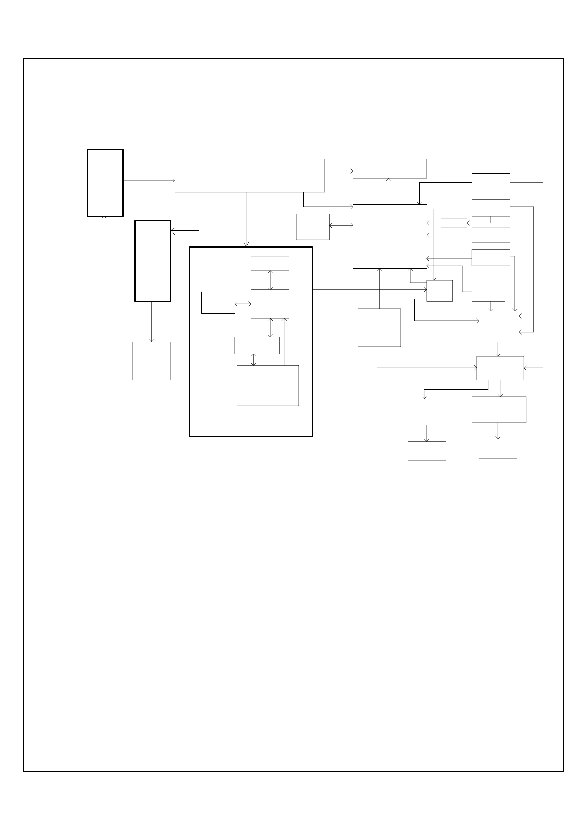
Part 1 Brief Introduction Of TheLVD-1902
Schematic Diagram
DIANYUAN
POWER SOURCE 100---240V AC 47HZ--63HZ 1.5A MAX
16V
IN
INVERTER
4 CCFL
BACKLIGHT
POWER
SUPPLY:16V
16V
K4S641632H
SD-RAM
DVD
、5V、
16V 5V
MOTOR DRIVER
3.3V、1.8V
MX29LV160
FLASH
MTK1389DE
DECODER
BA5954
LOADER
AT49F040A
FLASH
3.3V
YPBPR
L R
5V
1.8V
PANEL
LVDS
FLI8125
DECODER
AND
SCALER
CVBS
TUNER
RGB/YUV
SIF
BH3547
AMPLIFIER
PHONE
RGB/CVBS
CVBS
FSAV330
VEDIO
SWITCH
R G B
74LVC125
Y C
YPBPR
SCART
PC IN
HSI VSI
AV IN
SVHS IN
YPBPR
L\R
IN
AUDIO SWITCH
L R
VHC4052
L R
MPS3415
TPA3008
AMPLIFIER
SPEAKER
L R
L R
L R
Page 3
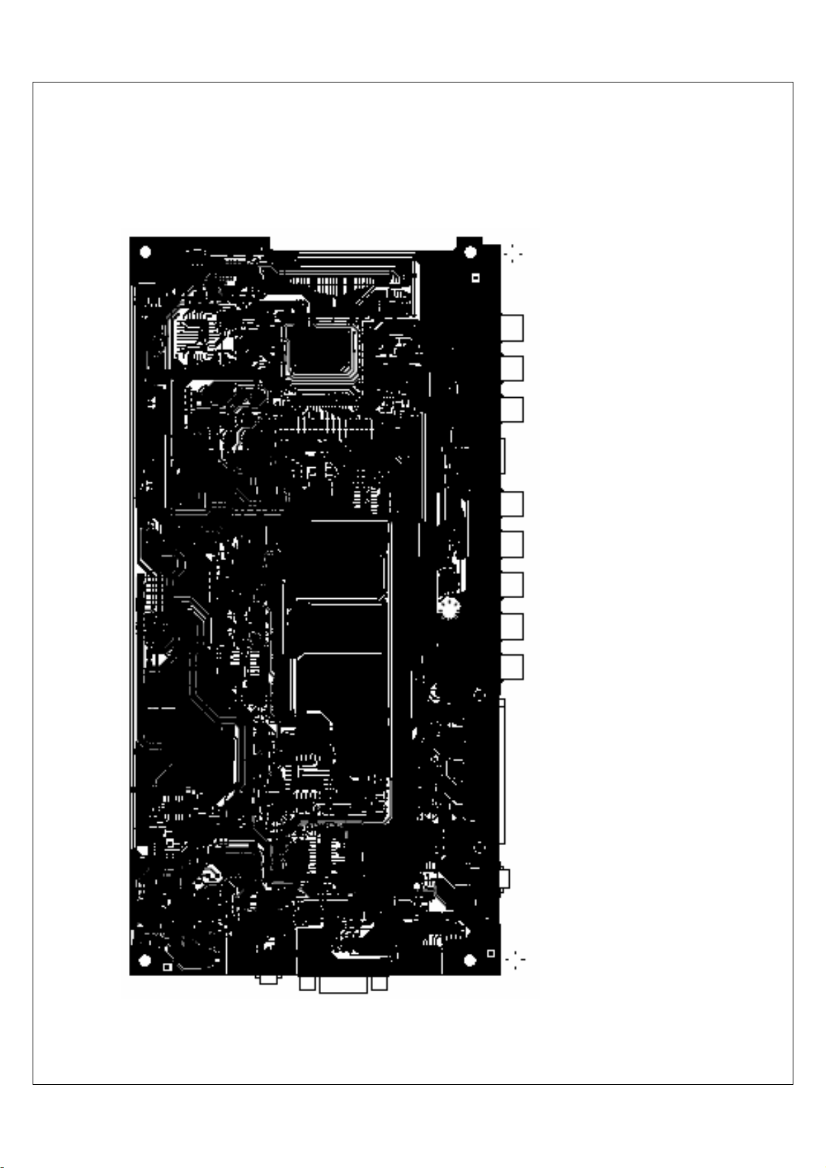
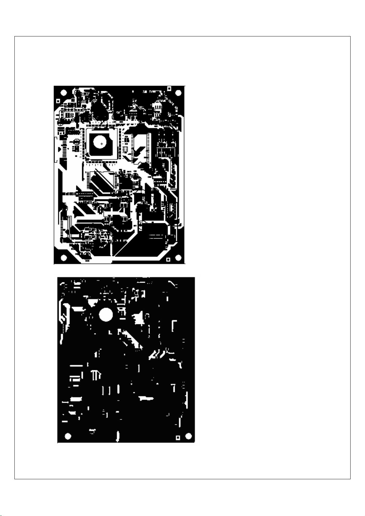
1. Main board
A: TOP LAYER
Printed Circuit
Page 4
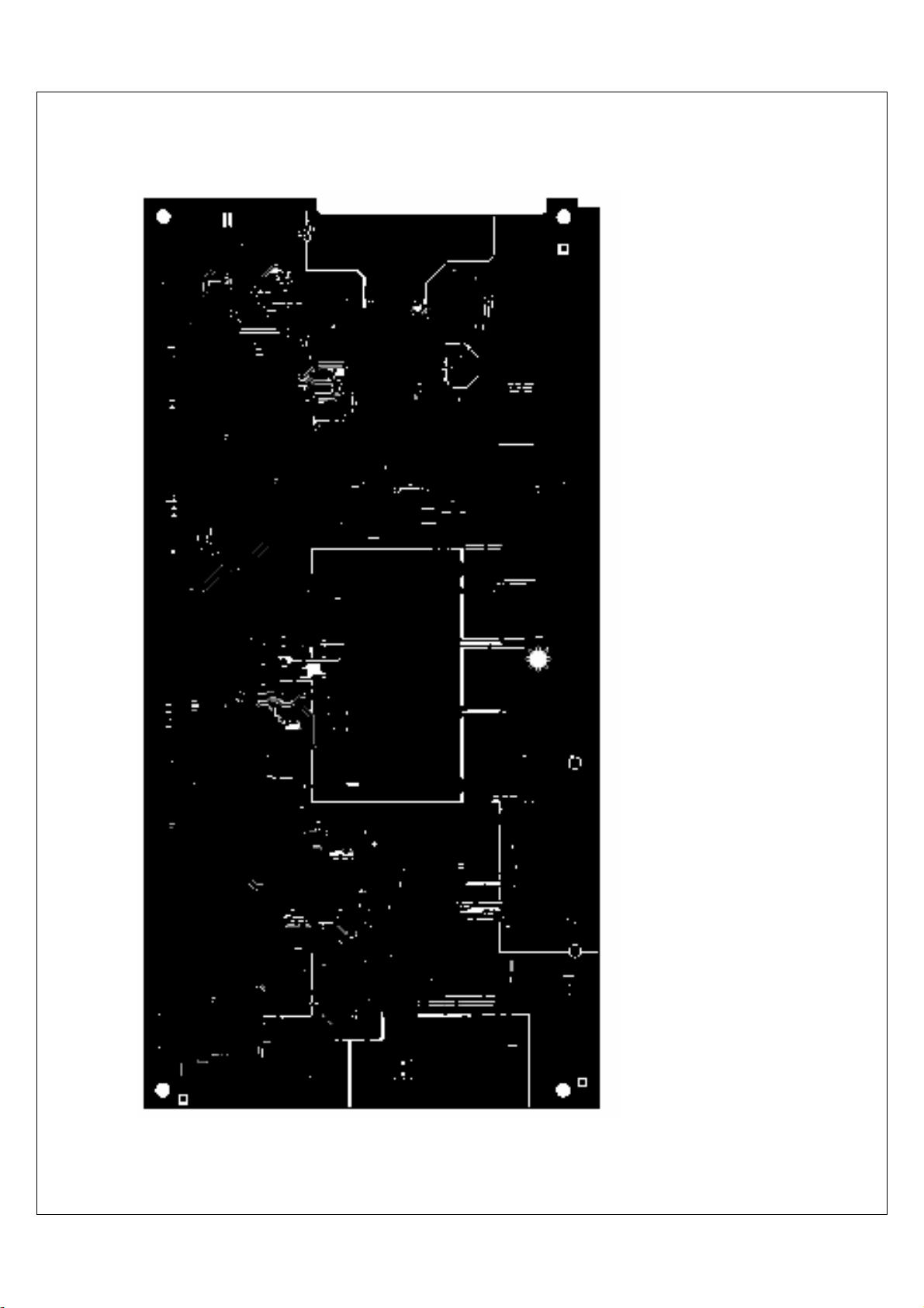
B: BOTTOM LAYER
Page 5
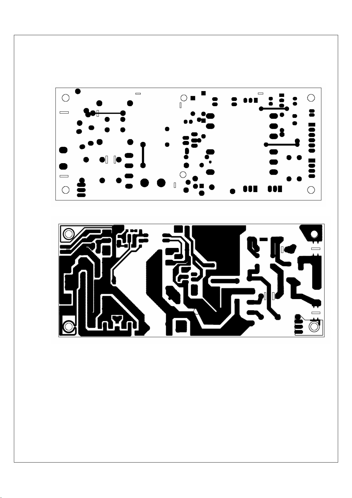
2. DVD board
A: TOP LAYER
B: BOTTOM LAYER
Page 6
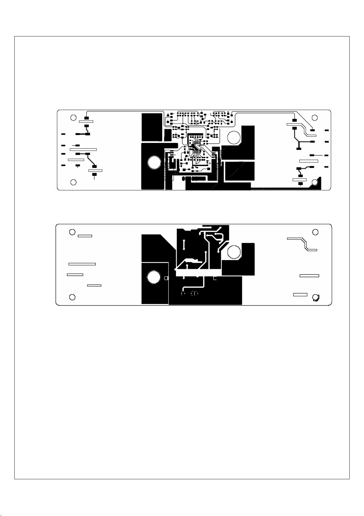
3. Power board
A: TOP LAYER
B: BOTTOM LAYER
Page 7
4. Inverter board
A: TOP LAYER
B: BOTTOM LAYER
Page 8
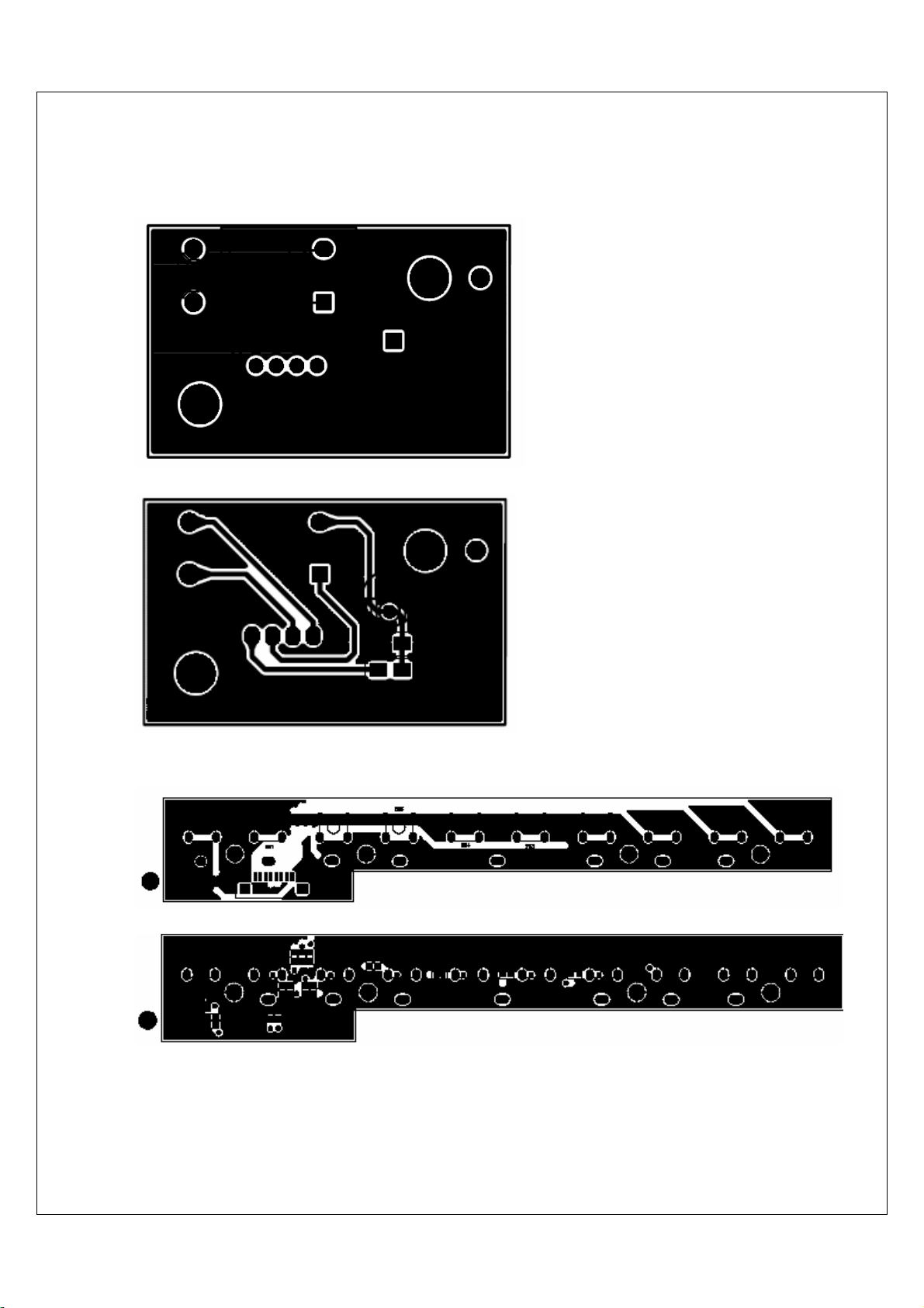
5. Remote Control Board
A: TOP LAYER
B: BOTTOM LAYER
6. Key board
A: TOP LAYER
B: BOTTOM LAYER
Page 9
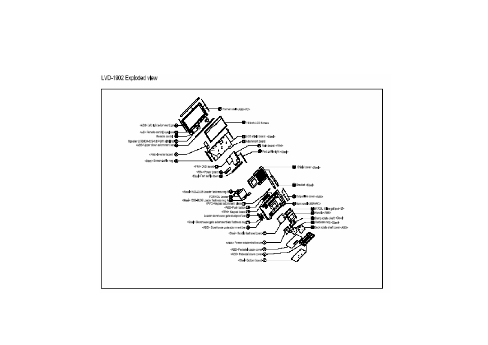
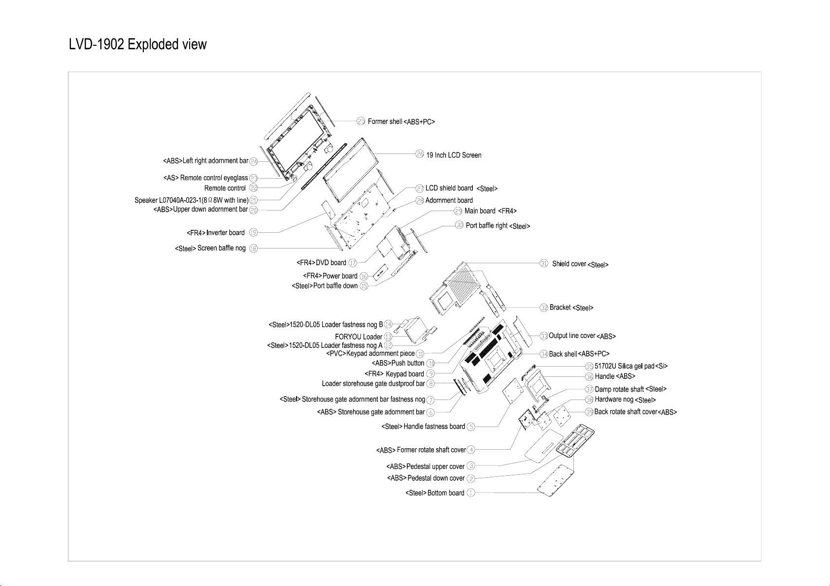
Exploded vi ew
Part 2 Exploded view
Page 10
Page 11
Part 3 Key ICs And Assemblies
On Main Board On DVD board
Serial
No
Position Type
1 3U7 78L09 1 U2 BA033
2 4U5 LM1117MPX-3.3V 2 U3 AZ1117H-1.8V
3 2U3 4U6 FDS9435 3 U6 MT1389DE/E
4 4U2 AIC1084(3.3V) 4 U4 BA5954FP
5 4U1 TL494C 5 U5 BA6287
6 4U3 LM1117DTX-1.8V 6 U8 IS42S16400B-7T
7 3U4 CD4052 7 U9 MX29LV160BBTC-70
8 3U1 MSP3415G 8 U7 24C16
9 1U4 AT24C32AN 9 U11 NJM4558
10 1U1 FSAV330 10 U10 CS4344
11 2U1 AT49BV040B 11 U1 78L05
12 2U5 FLI8125-LF
13 3U6 TPA3008D2PHP
14 1U3 24C02
15 3U9 BH3547F
16
1U7 1U6 1U8 1U9 1U11 1U12 1U13
1U15
PESD5V0L5
On Power Board On Inverter Board
1 U5 FSCM0765RGWDTU 1 1C1 Bit3193
2 U2 PC817
3 U3 KA431AZ
Serial
no
Position Type
Page 12
ICS ON MAIN BOARD
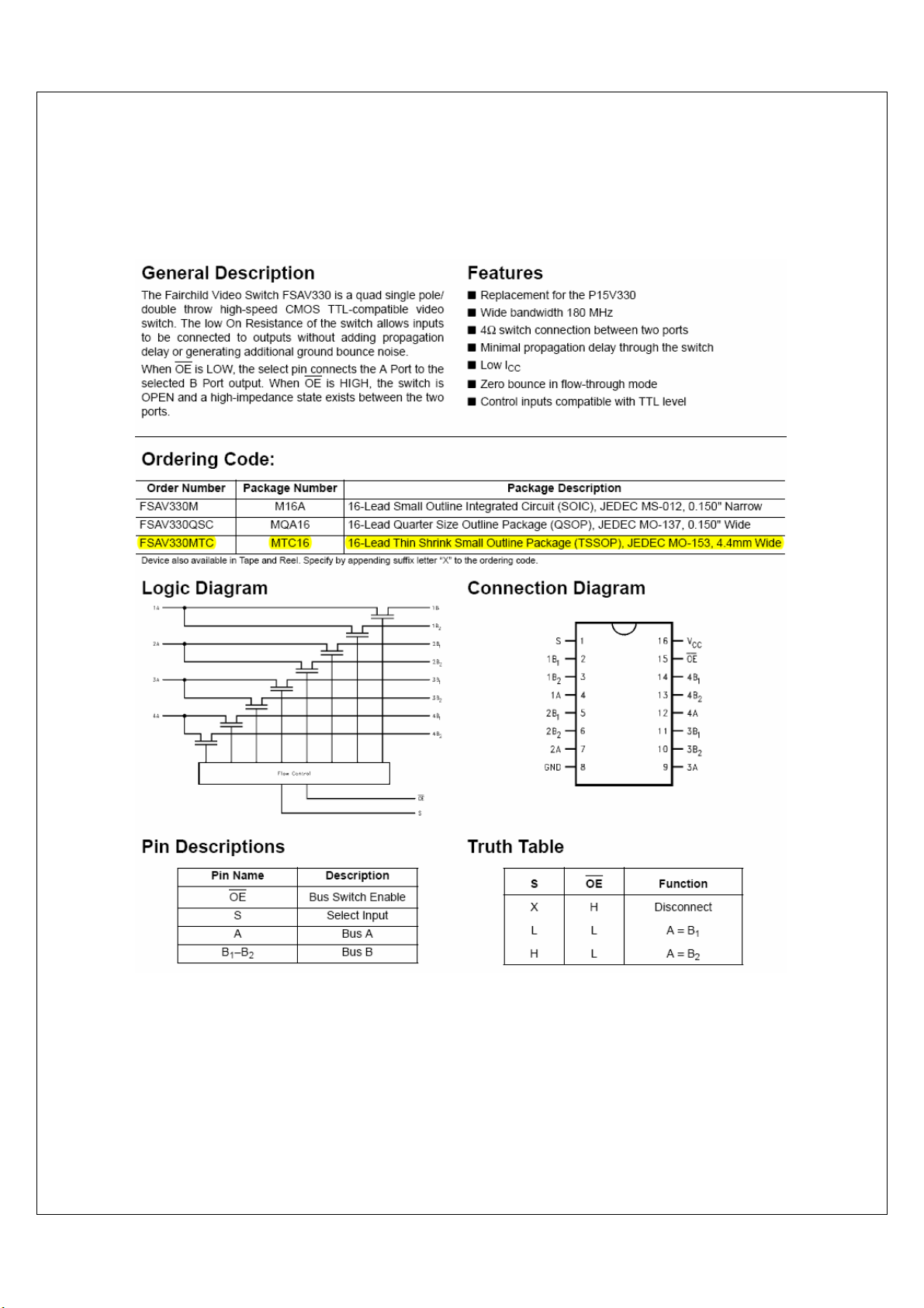
1. FSAV330
Low On Resistance Quad SPDT Wide Bandwidth Video Switch
Page 13
2. 74LVX125
Low Voltage Quad Buffer with 3-STATE Outputs.
Page 14
3. A T49BVO40B
Page 15
Page 16
Page 17
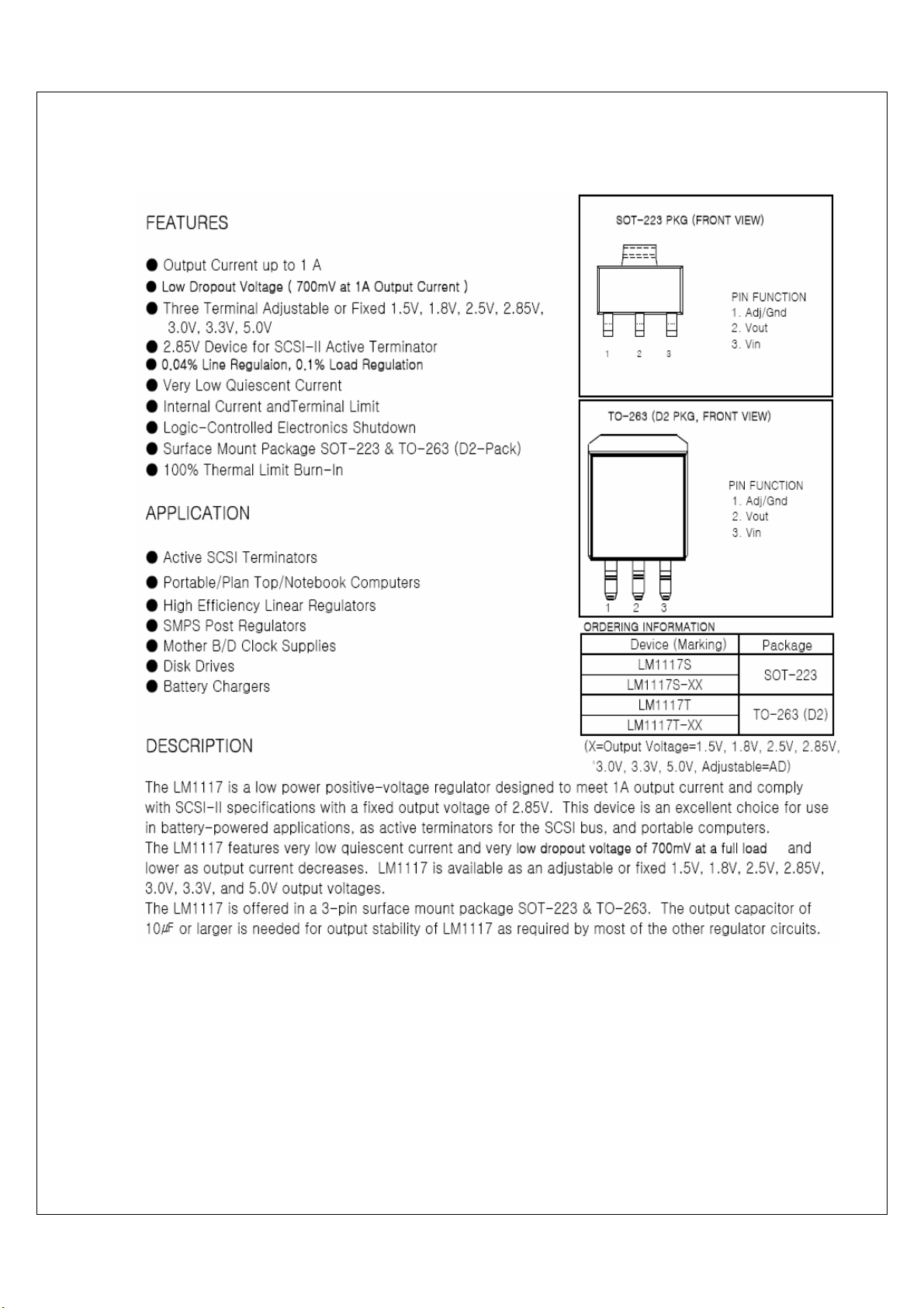
4. LM1117
Page 18
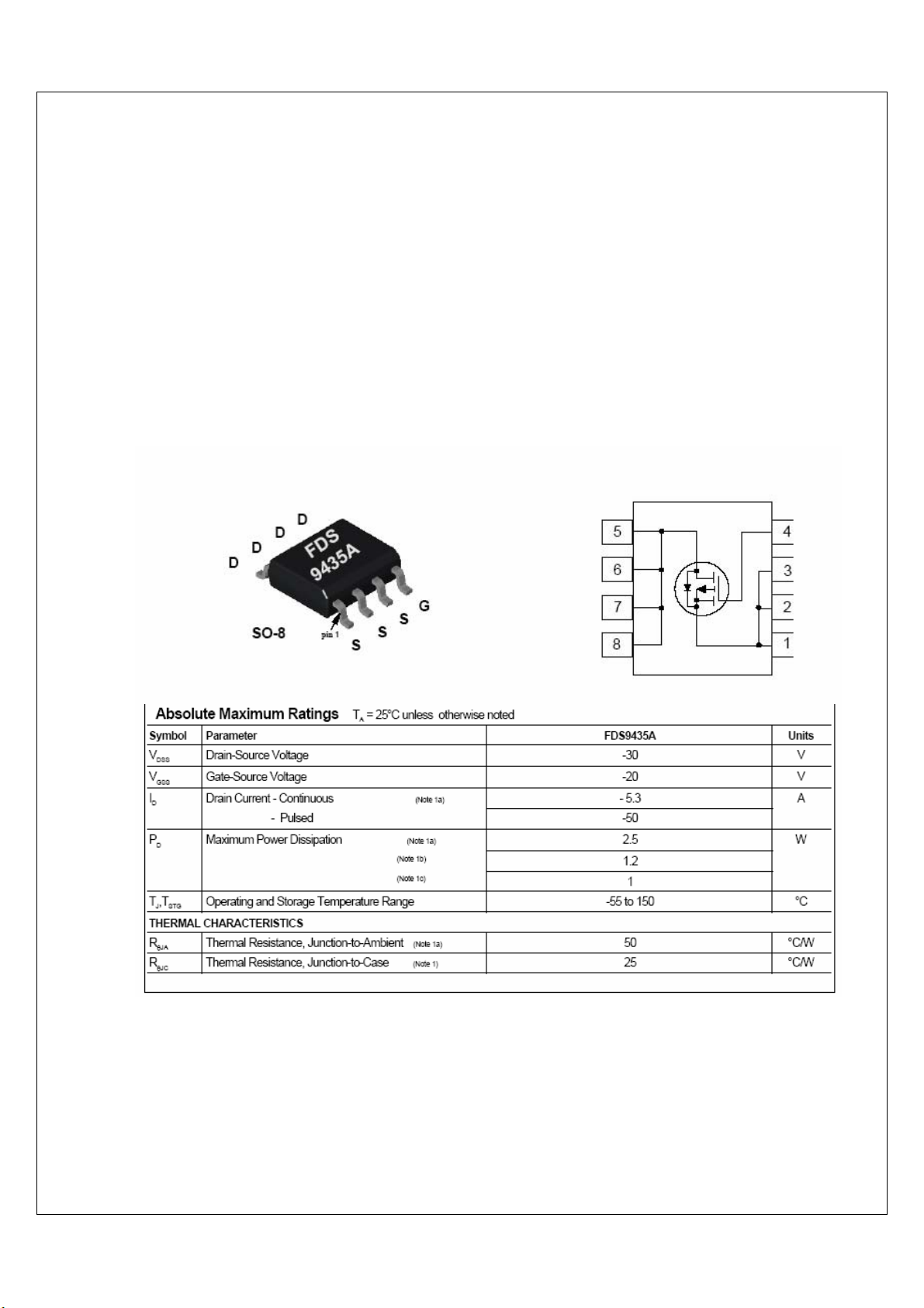
5. FDS9435A
Single P-Channel Enhancement Mode Field Effect Transistor
SO-8 P-Channel enhancement mode power field effect transistors are produced using
Fairchild's proprietary, high cell density, DMOS technology. This very high density process is
especially tailored to minimize on-state resistance and provide superior switching
performance. These devices are particularly suited for low voltage applications such as
notebook computer power management and other battery powered circuits where fast
switching, low in-line power loss, and resistance to transients are needed.
·Features
-5.3 A, -30 V, R
R
High density cell design for extremely low RDS(ON).
High power and current handling capability in a widely used surface mount package.
= 0.045 Ω @ VGS = -10 V,
DS(ON)
= 0.075 Ω @ VGS = - 4.5 V.
DS(ON)
Page 19
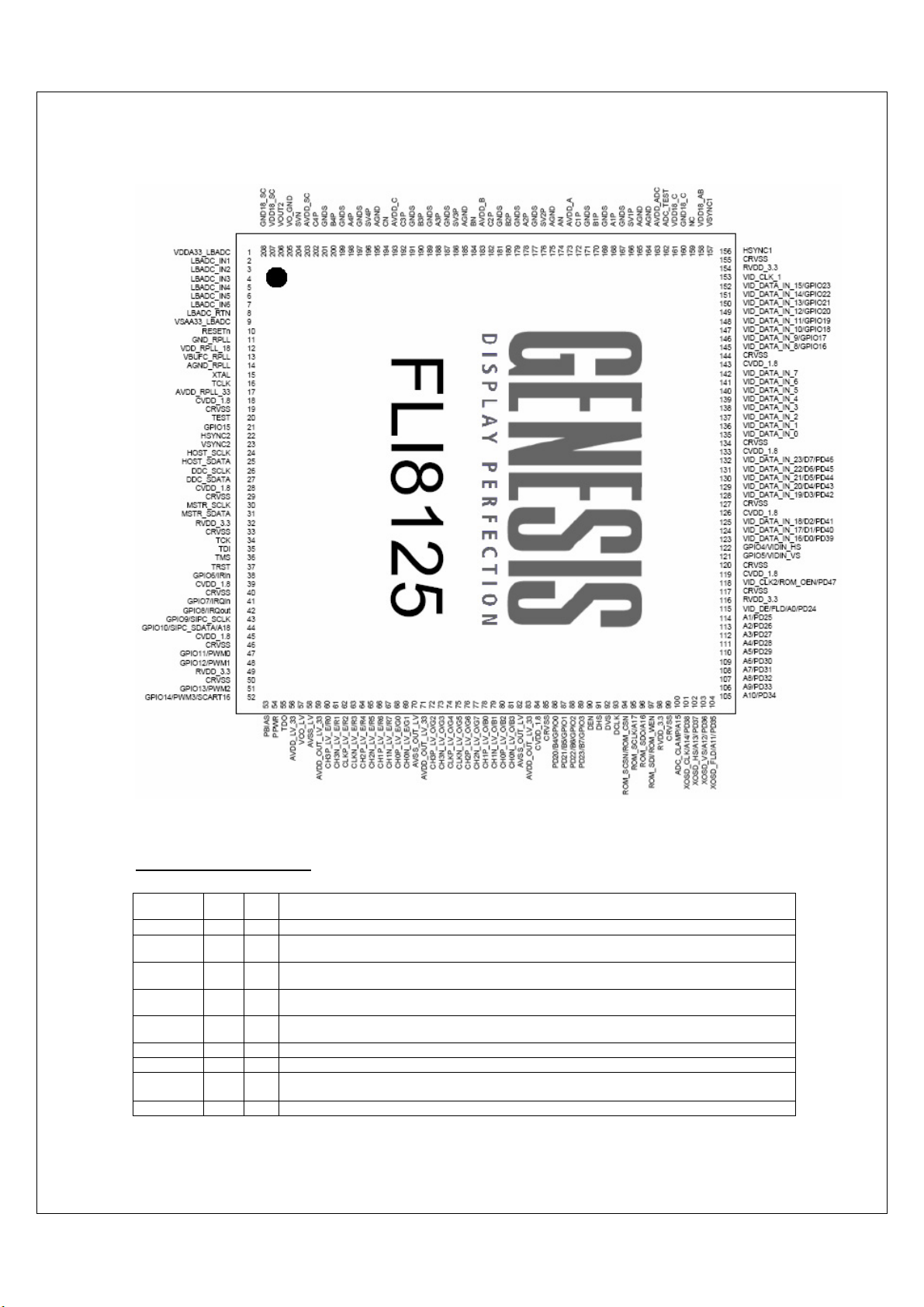
6.FLI8125
The FLI8125 is a cost-effective, highly-integrated, mixed signal solution for TV and Digit al
Video applications. It incorporates a multi-standard video decoder, high-speed triple 8 -bit
Analog-to-Digital Converter(ADC),and front end switching. An integrated VBI Slicer adds
Closed Captioning(CC) and Teletext service support, and the built-in microprocessor enables
full system control without external devices.
Features
Page 20
·PInput
·Pin List
I/O Legend: A = Analog, I = Input, O = Output, P = Power, G= Ground
Table 1: Analog Input Port
Pin Name No. I/O Description
VDD18_A
B
NC 159 No Connection. Leave this pin open for normal operation.
GND18_C 160 AG Analog Ground (1.8V Return) for C channel. Must be directly connected to the analog system ground plane
VDD18_C 16 1 AP Analog Power (1.8V) for C Channel. Must be bypassed with 0.1uF capacitor to the analog system ground
ADC_TES
T
AVDD_AD
C
AGND 164 AG Analog Ground. Must be directly connected to the analog system ground plane on board.
AGND 165 AG Analog Ground. Must be directly connected to the analog system ground plane on board.
SV1P 166 AI Positive analog sync input for channel 1.
GNDS 167 AG Analog Ground. Must be directly connected to the analog system ground plane on board.
158 AP Analog Power (1.8V) for A & B Channels. Must be bypassed with 0.1uF capacitor to the analog system
162 O Analog Front End Test O/P. Leave this Pin open. Used for factory testing purpose only.
163 AP Analog Power (3.3V) for ADC. Must be bypassed with 0.1uF capacitor to the analog system ground plane.
ground plane.
on board.
plane.
The input has to be AC coupled using a series 20 Ohm resistor and 0.1uF Capacitor network.
Page 21
A1P 168 AI Positive analog input ‘A’ for channel 1.
GNDS 169 AG Analog Ground. Must be directly connected to the analog system ground plane on board.
B1P 170 AI Positive analog input ‘B’ for channel 1.
GNDS 171 AG Analog Ground. Must be directly connected to the analog system ground plane on board.
C1P 172 AI Positive analog input ‘C’ for channel 1.
AVDD_A 173 AP Analog Power (3.3V) for ADC of Channel-A. Must be bypassed with 0.1uF capacitor to the analog system
AN 174 AI Nega t ive analog input ‘A’ for channels 1 through 4.
AGND 175 AG Analog Ground. Must be directly connected to the analog system ground plane on board.
SV2P 176 AI Positive analog sync input for channel 2.
GNDS 177 AG Analog Ground. Must be directly connected to the analog system ground plane on board.
A2P 178 AI Positive analog input ‘A’ for channel 2.
GNDS 179 AG Analog Ground. Must be directly connected to the analog system ground plane on board.
B2P 180 AI Positive analog input ‘B’ for channel 2.
GNDS 181 AG Analog Ground. Must be directly connected to the analog system ground plane on board.
C2P 182 AI Positive analog input ‘C’ for channel 2.
AVDD_B 183 AP Analog Power (3.3V) for ADC of Channel-B. Must be bypassed with 0.1uF capacitor to the analog system
BN 184 AI Nega t ive analog input ‘B’ for channels 1 through 4.
AGND 185 AG Analog Ground. Must be directly connected to the analog system ground plane on board.
SV3P 186 AI Positive analog sync input for channel 3.
VDD18_AB 158 AP Analog Power (1.8V) for A & B Channels. Must be bypassed with 0.1uF capacitor to the analog system
GNDS 187 AG Analog Ground. Must be directly connected to the analog system ground plane on board.
A3P 188 AI Positive analog input ‘A’ for channel 3.
GNDS 189 AG Analog Ground. Must be directly connected to the analog system ground plane on board.
B3P 190 AI Positive analog input ‘B’ for channel 3.
GNDS 191 AG Analog Ground. Must be directly connected to the analog system ground plane on board.
C3P 192 AI Positive an alog input ‘C’ for channel 3.
AVDD_C 193 AP Analog Power (3.3V) for ADC of Channel-C. Must be bypassed with 0.1uF capacitor to the analog system
CN 194 AI Negative analog input ‘C’ for channels 1 through 4.
The input has to be AC coupled using a series 20 Ohm resistor and 0.1uF Capacitor network.
The input has to be AC coupled using a series 20 Ohm resistor and 0.1uF Capacitor network.
The input has to be AC coupled using a series 20 Ohm resistor and 0.1uF Capacitor network.
ground plane.
This acts as the return Path for the Sources connected to Channel-A Inputs. This has to be AC coupled
using a series 20 Ohm resistor and 0.1uF Capacitor network to Analog Ground Plane on board.
The input has to be AC coupled using a series 20 Ohm resistor and 0.1uF Capacitor network.
The input has to be AC coupled using a series 20 Ohm resistor and 0.1uF Capacitor network.
The input has to be AC coupled using a series 20 Ohm resistor and 0.1uF Capacitor network.
The input has to be AC coupled using a series 20 Ohm resistor and 0.1uF Capacitor network.
ground plane.
This acts as the return Path for the Sources connected to Channel-B Inputs. This has to be AC coupled
using a series 20 Ohm resistor and 0.1uF Capacitor network to Analog Ground Plane on board.
The input has to be AC coupled using a series 20 Ohm resistor and 0.1uF Capacitor network.
ground plane.
The input has to be AC coupled using a series 20 Ohm resistor and 0.1uF Capacitor network.
The input has to be AC coupled using a series 20 Ohm resistor and 0.1uF Capacitor network.
The input has to be AC coupled using a series 20 Ohm resistor and 0.1uF Capacitor network.
ground plane.
This acts as the return Path for the Sources connected to Channel-C Inputs. This has to be AC coupled
using a series 20 Ohm resistor and 0.1uF Capacitor network to Analog Ground Plane on board.
AGND 195 AG Analog Ground. Must be directly connected to the analog system ground plane on board.
SV4P 196 AI Positive analog sync input for channel 4.
GNDS 197 AG Analog Ground. Must be directly connected to the analog system ground plane on board.
A4P 198 AI Positive analog input ‘A’ for channel 4.
GNDS 199 AG Analog Ground. Must be directly connected to the analog system ground plane on board.
B4P 200 AI Positive analog input ‘B’ for channel 4.
GNDS 201 AG Analog Ground. Must be directly connected to the analog system ground plane on board.
C4P 202 AI Positive an alog input ‘C’ for channel 4.
AVDD_SC 203 AP Analog Power (3.3V) for ADC of SYNC Channel. Must be bypassed with 0.1uF capacitor to the analog
The input has to be AC coupled using a series 20 Ohm resistor and 0.1uF Capacitor network.
The input has to be AC coupled using a series 20 Ohm resistor and 0.1uF Capacitor network.
The input has to be AC coupled using a series 20 Ohm resistor and 0.1uF Capacitor network.
The input has to be AC coupled using a series 20 Ohm resistor and 0.1uF Capacitor network.
system ground plane.
Page 22
SVN 204 AI Negative analog sync input for channels 1 through 4.
VO_GND 205 AG Analog Ground. Must be directly connected to the analog system ground plane on board.
VOUT2 206 AO Analog VOUT signal
VDD18_SC 207 AP Analog Power (1.8V) for SYNC Channel. Must be bypassed with 0.1uF capacitor to the analog system
GND18_SC 208 AG Analog Ground (1.8V Return) for SYNC channel. Must be directly connected to the analog system ground
This acts as the return Path for the Sources connected to SV Channel Inputs. This has to be AC coupled
using a series 20 Ohm resistor and 0.1uF Capacitor network to Analog Ground Plane on board.
This is the Analog Video Output from the Decoder in the Composite Video format. This can be amplified
and be fed to any video display device.
ground plane.
plane on board.
Table 2: Low Bandwidth ADC Input Port
Pin Name No I/O Description
VDDA33_LBADC 1 AP Analog Power (3.3V) for Low Bandwidth ADC Block. Must be bypassed with 0.1uF capacitor.
LBADC_IN1 2 AI Low Bandwidth Analog Input-1. The Input signal connected to this Pin, must be bypassed with a 0.1uF
LBADC_IN2 3 AI Low Bandwidth Analog Input-2. The Input signal connected to this Pin, must be bypassed with a 0.1uF
LBADC_IN3 4 AI Low Bandwidth Analog Input-3. The Input signal connected to this Pin, must be bypassed with a 0.1uF
LBADC_IN4 5 AI Low Bandwidth Analog Input-4. The Input signal connected to this Pin, must be bypassed with a 0.1uF
LBADC_IN5 6 AI Low Bandwidth Analog Input-5. The Input signal connected to this Pin, must be bypassed with a 0.1uF
LBADC_IN6 7 AI Low Bandwidth Analog Input-6. The Input signal connected to this Pin, must be bypassed with
LBADC_RTN 8 AG This Pin provides the Return Path for LBADC inputs. Must be directly connected to the analog system
VSSA33_LBADC 9 AG Analog Ground for Low Bandwidth ADC Block. Must be directly connected to the analog system ground
capacitor and could be in the range of 0V to 3.3V (peak to peak).
capacitor and could be in the range of 0V to 3.3V (peak to peak).
capacitor and could be in the range of 0V to 3.3V (peak to peak).
capacitor and could be in the range of 0V to 3.3V (peak to peak).
capacitor and could be in the range of 0V to 3.3V (peak to peak).
ground plane on board.
plane on board.
Table 3: RCLK PLL Pins
Pin Name No I/O Description
GND_RPLL 11 DG Digital GND for ADC clocking circuit. Must be directly connected to the digital system ground plane.
VDD_RPLL_18 12 DP Digital power (1.8V) for ADC digital logic. Must be bypassed with capacitor to Ground Plane.
VBUFC_RPLL 13 O Test Output. Leave this Pin Open. This is reserved for Factory Testing Purpose.
AGND_RPLL 14 AG Analog ground for the Reference DDS PLL. Must be directly connected to the analog system ground
XTAL 15 AO Crystal oscillator output.
TCLK 16 AI Reference clock (TCLK) from the 14.3MHz crystal oscillator.
AVDD_RPLL_33 17 AP Analog Power (3.3V) for RCLK PLL. Must be bypassed with 0.1uF capacitor.
plane.
Table 4: Digital Video Input Port
Pin Name No I/O Description
VID_CLK_1 153 I Video port data clock input meant for Video Input – 1. Up to 75Mhz
VIDIN_HS 122 I When Video Input – 1 is in BT656 Mode, this Pin acts as Horizontal Sync Input for Video Input – 2.
VIDIN_VS 121 I When Video Input – 1 is in BT656 Mode, this Pin acts as Vertical Sync Input for Video Input – 2.
VID_DATA_IN_0
VID_DATA_IN_1
VID_DATA_IN_2
VID_DATA_IN_3
VID_DATA_IN_4
VID_DATA_IN_5
VID_DATA_IN_6
VID_DATA_IN_7
Pin Name No I/O Description
135
136
137
138
139
140
141
142
[Input, 5V-tolerant]
OR when Video Input – 1 is in 16 Bit Mode this Pin acts as Horizontal Sync Input for Video Input – 1.
OR this Pin acts as Horizontal Sync Input for 24 Bit Video Input
OR when Video Input – 1 is in 16 Bit Mode this Pin acts as Vertical Sync Input for Video Input – 1.
OR this Pin acts as Vertical Sync Input for 24 Bit Video Input
IO Input YUV data in 8-bit BT656 of Video Input – 1
[Bi-Directional, 5V-tolerant]
OR Input Y Data in case of 16 Bit Video Input (CCIR601) of Video Input – 1
OR Input Red Data in case of 24 Bit Video Input
Page 23
VID_DATA_IN_8
VID_DATA_IN_9
VID_DATA_IN_10
VID_DATA_IN_11
VID_DATA_IN_12
VID_DATA_IN_13
VID_DATA_IN_14
VID_DATA_IN_15
VID_DATA_IN_16
VID_DATA_IN_17
VID_DATA_IN_18
VID_DATA_IN_19
VID_DATA_IN_20
VID_DATA_IN_21
VID_DATA_IN_22
VID_DATA_IN_23
VID_CLK2 118 I Video port data clock input meant for Video Input – 2. Up to 75Mhz
VID_DE/FLD 115 I Video Active Signal Input or the Field Signal Input from external Digital Video Source.
145
IO Input Pr / Pb Data in case of 16 Bit Video Input (CCIR601) of Video Input – 1
146
147
148
149
150
151
152
123
124
125
128
129
130
131
132
OR Input Green Data in case of 24 Bit Video Input
IO Input Blue Data in case of 24 Bit Video Input
OR Video Input – 2 in 8-bit with Embedded Sync / Separate Sync Sync in which case
VID_DATA_IN_16 acts as the LSB of the 8-bit Video input and VID_DATA_IN_23 acts as the MSB of
the 8-bit Video input.
[Input, 5V-tolerant]
Note: In case of Multiple Digital Video Input Sources, only one source could be in 8-Bit with
embedded Sync (BT656 mode) format.
Table 5: System Interface
Pin Name No I/O Description
RESETn 10 I Hardware Reset (active low) [Schmitt trigger, 5v-tolerant]
TEST 20 I For normal mode of operation connect this Pin to Ground.
GPIO15 21 IO This pin is available as a general-purpose input/output port. Also it is optionally programmable to
Connect to ground with 0.01uF (or larger) capacitor.
give out the external chip select signal meant for external SRAM. Refer to note below.
HSYNC2 22 I Horizontal Sync signal Input-2. Used when Analog RGB component signal carries separate
VSYNC2 23 I Vertical Sync signal Input-2. Used when Analog RGB component signal carries separate VSYNC
HOST_SCLK 24 IO Host input clock or 186 UART Data In or JTAG clock signal.
HOST_SDATA 25 IO Host input data or 186 UART Data Out or JTAG mode signal.
DDC_SCLK 26 IO
DDC_SDATA 27 IO
MSTR_SCLK 30 O Clock signal from Master Serial 2 Wire Interface Controller
MSTR_SDATA 31 IO Data signal meant for Master Serial 2 Wire interface Controller
TCK 34 IO This Pin accepts the Input Clock signal in case of Boundary Scan Mode.
TDI 35 IO This Pin accepts the Input Data signal in case of Boundary Scan Mode.
TMS 36 IO This Pin accepts the Input Test Mode Select signal in case of Boundary Scan Mode.
TRST 37 IO This Pin accepts the Boundary Scan Reset signal in case of Boundary Scan Mode.
GPIO6/IRin 38 IO Input from Infra Red Decoder can be connected to this Pin. When not used, this pin is available
GPIO7/IRQin 41 IO Input Interrupt Request signal can be connected to this Pin. When not used, this pin is available
GPIO8/IRQout 42 IO This Pin will give out the Interrupt Signal to interrupt external Micro. When not used, this pin is
GPIO9/SIPC_SCLK 43 IO This Pin accepts the Clock signal from External Serial 2 Wire interface Bus if FLI8125 is
GPIO10/SIPC_SDATA/
A18
GPIO11/PWM0 47 IO This Pin can be programmed to give out Pulse Width Modulated Output Pulses for external use.
GPIO12/PWM1 48 IO This Pin can be programmed to give out Pulse Width Modulated Output Pulses for external use.
GPIO13/PWM2 51 IO This Pin can be programmed to give out Pulse Width Modulated Output Pulses for external use.
Pin Name No I/O Description
44 IO This Pin acts as the Data I/O signal when used with External Serial 2 Wire interface Bus if
HSYNC signal.
signal.
[Input, Schmitt trigger, 5V-tolerant]
[Bi-directional, Schmitt trigger, slew rate limited, 5V-tolerant]
DDC2Bi clock for VGA Port [internal 10KΩ pull-up resistor]
DDC2Bi data for VGA Port [internal 10KΩ pull-up resistor]
as General Purpose Input/output Port.
as General Purpose Input/output Port.
available as General Purpose Input/output Port.
programmed to be in Slave mode. When not used, this pin is available as General Purpose
Input/output Port.
FLI8125 is programmed to be in Slave mode. Or this Pin is programmable to give out Address #
18 from the Internal Micro when used with 512K External Memory. When not used, this pin is
available as General Purpose Input/output Port.
When not used, this pin is available as General Purpose Input/output Port.
When not used, this pin is available as General Purpose Input/output Port.
When not used, this pin is available as General Purpose Input/output Port.
Page 24
GPIO14/PWM3/
SCART16
TDO 55 O This Pin provides the Output Data in case of Boundary Scan Mode.
HSYNC1 156 I Horizontal Sync signal Input-1. Used when Analog RGB component signal carries separate
VSYNC1 157 I Vertical Sync signal Input-1. Used when Analog RGB component signal carries separate VSYNC
101 O Clock Output meant for External OSD Controller
102 O Horizontal Sync Output meant for External OSD Controller
XOSD_CLK 103 O Vertical Sync Output meant for External OSD Controller
XOSD_HS 104 O Field Signal Output meant for External OSD Controller
PD20/B4/GPIO0
PD21/B5/GPIO1
PD22/B6/GPIO2
PD23/B7/GPIO3
52 IO This Pin can be programmed to give out Pulse Width Modulated Output Pulses for external use.
86
87
88
89
Or it can be programmed to sense the Fast Blank Input signal from a SCART I/P source. When
not used, this pin is available as General Purpose Input/output Port.
HSYNC signal.
signal.
IO T hese Pins provide the Panel Data as shown in the TTL Display Interface Table below. These are
available as General Purpose Input / Output Pins when not used as Panel Data.
Table 6: LVDS Display Interface
Pin Name No I/O Description
PBIAS 53 O Panel Bias Control (backlight enable) [Tri-state output, 5V- tolerant]
PPWR 54 O Panel Power Control [Tri-state output, 5V- tolerant]
AVDD_LV_33
VCO_LV
AVSS_LV
AVDD_OUT_LV_33
CH3P_LV_E
CH3N_LV_E
CLKP_LV_E
CLKN_LV_E
CH2P_LV_E
CH2N_LV_E
CH1P_LV_E
CH1N_LV_E
CH0P_LV_E
CH0N_LV_E
AVSS_OUT_LV
AVDD_OUT_LV_33
CH3P_LV_O
CH3N_LV_O
CLKP_LV_O
CLKN_LV_O
CH2P_LV_O
CH2N_LV_O
CH1P_LV_O
CH1N_LV_O
CH0P_LV_O
CH0N_LV_O
AVSS_OUT_LV
AVDD_OUT_LV_33
56 DP Digital Power for LVDS Block. Connect to digital 3.3V supply.
57 O Reserved. Output for Testing Purpose only at Factory.
58 G Ground for LVDS outputs.
59 DP Digital Power for LVDS outputs. Connect to digital 3.3V supply.
60 O
61 O
62 O
63 O
64 O
65 O
66 O
67 O
68 O
69 O
70 G Ground for LVDS outputs.
71 DP Digital Power for LVDS outputs. Connect to digital 3.3V supply.
72 O
73 O
74 O
75 O
76 O
77 O
78 O
79 O
80 O
81 O
82 G Ground for LVDS outputs.
83 DP Digital Power for LVDS outputs. Connect to digital 3.3V supply.
These form the Differential Data Output for Channel – 3 (Even).
These form the Differential Clock Output Even Channel.
These form the Differential Data Output for Channel – 2 (Even).
These form the Differential Data Output for Channel – 1 (Even).
These form the Differential Data Output for Channel – 0 (Even).
These form the Differential Data Output for Channel – 3 (Odd).
These form the Differential Clock Output Odd Channel.
These form the Differential Data Output for Channel – 2 (Odd).
These form the Differential Data Output for Channel – 1 (Odd).
These form the Differential Data Output for Channel – 0 (Odd).
Page 25
Table 7: TTL Display Interface
Pin Name No I/O Description
PBIAS 53 O Panel Bias Control (backlight enable) [Tri-state output, 5V- tolerant]
PPWR 54 O Panel Power Control [Tri-state output, 5V- tolerant]
AVDD_LV_33
VCO_LV
AVSS_LV
AVDD_OUT_LV_33
R0
R1
R2
R3
R4
R5
R6
R7
G0
G1
AVSS_OUT_LV
AVDD_OUT_LV_33
G2
G3
G4
G5
G6
G7
B0
B1
B2
B3
AVSS_OUT_LV
AVDD_OUT_LV_33
PD20/B4 86 O Blue channel bit 4 (Even) Blue channel bit 2 (Even)
PD21/B5 87 O Blue channel bit 5 (Even) Blue channel bit 3 (Even)
PD22/B6 88 O Blue channel bit 6 (Even) Blue channel bit 4 (Even)
PD23/B7 89 O Blue channel bit 7 (Even) Blue channel bit 5 (Even)
DEN 90 O Display Data Enable
DHS 91 O Display Horizontal Sync.
DVS 92 O Display Vertical Sync.
DCLK 93 O Display Pixel Clock
PD24
Pin Name No I/O Description
PD25
PD26
PD27
PD28
PD29
PD30
PD31
PD32
PD33
PD34
PD35
PD36
PD37
PD38
PD39
PD40
PD41
PD42
PD43
PD44
PD45
56 DP Digital Power for TTL Block. Connect to digital 3.3V supply.
57 O Reserved. Output for Testing Purpose only at Factory.
58 G Ground for TTL outputs.
59 DP Digital Power for TTL outputs. Connect to digital 3.3V supply.
60 O Red channel bit 0 (Even) Not used.
61 O Red channel bit 1 (Even) Not used.
62 O Red channel bit 2 (Even) Red channel bit 0 (Even)
63 O Red channel bit 3 (Even) Red channel bit 1 (Even)
64 O Red channel bit 4 (Even) Red channel bit 2 (Even)
65 O Red channel bit 5 (Even) Red channel bit 3 (Even)
66 O Red channel bit 6 (Even) Red channel bit 4 (Even)
67 O Red channel bit 7 (Even) Red channel bit 5 (Even)
68 O Green channel bit 0 (Even) Not used.
69 O Green channel bit 1 (Even) Not used.
70 G Ground for TTL outputs.
71 DP Digital Power for TTL outputs. Connect to digital 3.3V supply.
72 O Green channel bit 2 (Even) Green channel bit 0 (Even)
73 O Green channel bit 3 (Even) Green channel bit 1 (Even)
74 O Green channel bit 4 (Even) Green channel bit 2 (Even)
75 O Green channel bit 5 (Even) Green channel bit 3 (Even)
76 O Green channel bit 6 (Even) Green channel bit 4 (Even)
77 O Green channel bit 7 (Even) Green channel bit 5 (Even)
78 O Blue channel bit 0 (Even) Not used.
79 O Blue channel bit 1 (Even) Not used.
80 O Blue channel bit 2 (Even) Blue channel bit 0 (Even)
81 O Blue channel bit 3 (Even) Blue channel bit 1 (Even)
82 G Ground for TTL outputs.
83 DP Digital Power for TTL outputs. Connect to digital 3.3V supply.
115 O Red channel bit 0 (Odd) Not used.
114 O Red channel bit 1 (Odd) Not used.
113 O Red channel bit 2 (Odd) Red channel bit 0 (Odd)
112 O Red channel bit 3 (Odd) Red channel bit 1 (Odd)
111 O Red channel bit 4 (Odd) Red channel bit 2 (Odd)
110 O Red channel bit 5 (Odd) Red channel bit 3 (Odd)
109 O Red channel bit 6 (Odd) Red channel bit 4 (Odd)
108 O Red channel bit 7 (Odd) Red channel bit 5 (Odd)
107 O Green channel bit 0 (Odd) Not used.
106 O Green channel bit 1 (Odd) Not used.
105 O Green channel bit 2 (Odd) Green channel bit 0 (Odd)
104 O Green channel bit 3 (Odd) Green channel bit 1 (Odd)
103 O Green channel bit 4 (Odd) Green channel bit 2 (Odd)
102 O Green channel bit 5 (Odd) Green channel bit 3 (Odd)
101 O Green channel bit 6 (Odd) Green channel bit 4 (Odd)
123 O Green channel bit 7 (Odd) Green channel bit 5 (Odd)
124 O Blue channel bit 0 (Odd) Not used.
125 O Blue channel bit 1 (Odd) Not used.
128 O Blue channel bit 2 (Odd) Blue channel bit 0 (Odd)
129 O Blue channel bit 3 (Odd) Blue channel bit 1 (Odd)
130 O Blue channel bit 4 (Odd) Blue channel bit 2 (Odd)
131 O Blue channel bit 5 (Odd) Blue channel bit 3 (Odd)
For 8-bit panels For 6-bit panels
For 8-bit panels For 6-bit panels
24
Page 26

PD46
PD47
132 O Blue channel bit 6 (Odd) Blue channel bit 4 (Odd)
118 O Blue channel bit 7 (Odd) Blue channel bit 5 (Odd)
Note: In case of 24 Bit TTL Panels the RGB Odd Channel Outputs will not be used. In that case they can be
made available for other purposes as Address & Data from On-Chip Micro or Digital Video Input Data.
Table 8: Parallel/Serial ROM Interface
Pin Name No I/O Description
A17
A16
A15
A14
A13
A12
A11
A10
A9
A8
A7
A6
A5
A4
A3
A2
A1
A0
D7
D6
D5
D4
D3
D2
D1
D0
ROM_OEN 118 O External PROM data Output Enable.
ROM_SDI/
ROM_WEN
ROM_SCSN/
ROM_CSN
Table 9: Digital Power and Ground
Pin Name No I/O Description
RVDD_3.3 32 49 98 116 154 P Ring VDD. Connect to digital 3.3V.
95
O 256K x8 PROM Address. These pins also have bootstrap functionality.
96
100
101
102
103
104
105
106
107
108
109
110
111
112
113
114
115
132
131
130
129
128
125
124
123
97 O External PROM data Write Enable (for In-System-Programming of FLASH) or Serial Data Input
94 O External PROM data Chip Select or Serial PROM Chip Select (ROM_SCSN) for SPI ROM
For serial SPI ROM interface:
- ROM_ADDR17 will be Serial Clock (ROM_SCLK)
- ROM_ADDR16 will be Serial Data Output (ROM_SDO)
For 512K X 8 PROM, Address Signal A18 is available thru Pin # 44 which is GPIO10.
IO External PROM data input.
(SDI) for SPI ROM interface.
interface.
CVDD_1.8 18 28 39 45 84 119 126 133 143 P Core VDD. Connect to digital 1.8V.
CRVSS 19 29 33 40 46 50 85 99 117 120
127 134 144 155
G Chip ground for core and ring.
Table 10: JTAG Boundary Scan
Pin Name No I/O Description
TCK 34 I JTAG Boundary Scan TCK signal
TDO 55 O JTAG Boundary Scan TDO signal
TDI 35 I JTAG Boundary Scan TDI signal. Pad has internal 50K pull-up resistor.
TMS 36 I JTAG Boundary Scan RST signal. Pad has internal 50K pull-up resistor.
TRST 37 I JTAG Boundary Scan TMS signal. Pad has internal 50K pull-up resistor.
25
Page 27

7. CD4052B
The CD4052B is a differential 4-Channel multiplexer having two binary control inputs, A
and B, and an inhibit input. The two binary signals selec t 1 of 4 pairs of channels to be turned
on and connect the analog inputs to the outputs.
·PInputs
.
26
Page 28

8. A T24C32AN
2-Wire Serial EEPROM 32K (4096 x 8)
27
Page 29

28
Page 30

9. TPA3008D2
10-W STEREO CLASS-D AUDIO POWER AMPLIFIER.
29
Page 31

·Pin Description
30
Page 32

10. TL494
PULSE-WIDTH-MODULATION CONTROL CIRCUITS
31
Page 33

1. BA5954
ICS ON DVD BOARD
32
Page 34

33
Page 35

2. MT1389HD
Abbr. :
SR : Slew Rate
PU : Pull Up
PD : Pull Down
SMT : Schmitt Trigger
2MA~16MA : Output buffer driving strength.
Pin Main Alt. Type Description
231 RFGND18
232 RFVDD18
252 OSP
253 OSN
254 RFGC
Ground Analog ground
Analog output RF Offset cancellation capacitor connecting
Analog output RF Offset cancellation capacitor connecting
Analog output RF AGC loop capacitor connecting for DVD-ROM
255 IREF
Analog Input RF path. Connect an external 15K resistor to this pin and
Ground Analog ground
Analog Input AC coupled input path A
Analog Input AC coupled input path B
Analog Input AC coupled input path C
Analog Input AC coupled input path D
Analog Input AC coupled DVD RF signal input RFIP
Analog Input AC coupled DVD RF signal input RFIN
Analog Input DC coupled main-beam RF signal input A
Analog Input DC coupled main-beam RF signal input B
Analog Input DC coupled main-beam RF signal input C
Analog Input DC coupled main-beam RF signal input D
Analog Input DC coupled sub-beam RF signal input A
Analog Input DC coupled sub-beam RF signal input B
Analog Input DC coupled sub-beam RF signal input C
Analog Input DC coupled sub-beam RF signal input D
Analog Input CD focusing error negative input
Analog Input CD focusing error positive input
Analog Input 3 beam satellite PD signal negative input
Analog Input 3 beam satellite PD signal positive input
256 AVDD3
1 AGND
2 DVDA
3 DVDB
4 DVDC
5 DVDD
6 DVDRFIP
7 DVDRFIN
8 MA
9 MB
10 MC
11 MD
12 SA
13 SB
14 SC
15 SD
16 CDFON
17 CDFOP
18 TNI
19 TPI
RF Interface ( 26 )
Power Analog power 1.8V
Current reference input. It generates reference current for
AVSS.
Power Analog power 3.3V
ALPC ( 4 )
Pin Main Alt. Type Description
20 MDI1
21 MDI2
22 LDO2
23 LDO1
Analog Input Laser power monitor input
Analog Input Laser power monitor input
Analog Output Laser driver output
Analog Output Laser driver output
34
Page 36

ADC Power ( 2 )
244 ADCVDD3
245 ADCVSS
43 VPLLVSS
44 CAPPAD
45 VPLLVDD3
28 V2REFO
29 V20
30 VREFO
24 SVDD3
25 CSO RFOP Analog output
26 RFLVL RFON Analog output
27 SGND
31 FEO
32 TEO
33 TEZISLV
Power Analog 3.3V Power for ADC
Ground Analog ground for ADC
VPLL (3)
Ground Analog ground for VPLL
Analog Input VPLL External Capacitance connection
Power Analog 3.3V Power for VPLL
Reference Voltage ( 3 )
Analog output Reference voltage 2.8V
Analog output Reference voltage 2.0V
Analog output Reference voltage 1.4V
Analog Monitor Output ( 7 )
Power Analog power 3.3V
Ground Analog ground
Analog output Focus error monitor output
Analog output Tracking error monitor output
Analog output TE Slicing Level
1)
Central servo Positive main beam summing output
2)
1)
RFRP low pass, or Negative main beam summing
2)
output
246 RFVDD3
247 RFRPDC
248 RFRPAC
249 HRFZC
250 CRTPLP
251 RFGND
Analog Servo Interface ( 6 )
Power Analog Power
Analog output RF ripple detect output
Analog Input RF ripple detect input(through AC-coupling)
Analog Input High frequency RF ripple zero crossing
Analog output Defect level filter capacitor connecting
Ground Analog Power
35
Page 37

RF Data PLL Interface ( 9 )
Pin Main Alt. Type Description
235 JITFO
236 JITFN
237 PLLVSS
238 IDACEXLP
239 PLLVDD3
240 LPFON
241 LPFIP
242 LPFIN
243 LPFOP
Analog output The output terminal of RF jitter meter.
Analog Input The input terminal of RF jitter meter.
Ground Ground pin for data PLL and related analog circuitry.
Analog output Data PLL DAC Low-pass filter
Power Power pin for data PLL and related analog circuitry.
Analog Output The negative output of loop filter amplifier
Analog Input The positive input terminal of loop filter amplifier.
Analog Input The negative input terminal of loop filter amplifier.
Analog Output The positive output of loop filter amplifier
Motor and Actuator Driver Interface ( 10 )
34 OP_OUT
35 OP_INN
36 OP_INP
37 DMO
38 FMO
39
40
41 TRO
42 FOO
50
55,93,
142,160,
174, 213
81,178 DVSS
65,96,11
8,
131,145,
156,
170, 208
90, 148 DVSS
TROPENP
W M
PWMOUT
FG (Digital
pin)
DVDD18
DVDD3
1
V_ADIN9 Analog Output
V_ADIN8
Analog output Op amp output.
Analog input Op amp negative input
Analog input Op amp positive input
Analog Output Disk motor control output. PWM output.
Analog Output Feed motor control. PWM output.
Analog Output Tray PWM output / Tray open output.
Analog Output
Analog Output
LVTTL 3.3V Input,
Schmitt Input, pull
up , with analog
input path for
V_ADIN8
General Power/Ground ( 18 )
Power 1.8V power pin for internal digital circuitry
Ground 1.8V Ground pin for internal digital circuitry
Power 3.3V power pin for internal digital circuitry
Ground 3.3V Ground pin for internal digital circuitry
1)
2)
Tracking servo output. PDM output of tracking servo
compensator.
Focus servo output. PDM output of focus servo
compensator
1)
2)
1st General PWM output, or
Version AD input 9
Motor Hall sensor input, or
Version AD input 8
Micro Controller and Flash Interface (48)
Pin Main Alt. Type Description
36
Page 38

62 HIGHA0
Input
2~16MA, SR
PU
Microcontroller address 8
74 HIGHA1
73 HIGHA2
72 HIGHA3
71 HIGHA4
70 HIGHA5
69 HIGHA6
68 HIGHA7
Input
2~16MA, SR
PU
Input
2~16MA, SR
PU
Input
2~16MA, SR
PU
Input
2~16MA, SR
PU
Input
2~16MA, SR
PU
Input
2~16MA, SR
PU
Input
2~16MA, SR
PU
Microcontroller address 9
Microcontroller address 10
Microcontroller address 11
Microcontroller address 12
Microcontroller address 13
Microcontroller address 14
Microcontroller address 15
89 AD7
86 AD6
85 AD5
84 AD4
83 AD3
82 AD2
80 AD1
79 AD0
92 IOA0
Input 2~16MA, SR
Input 2~16MA, SR
Input 2~16MA, SR
Input 2~16MA, SR
Input 2~16MA, SR
Input 2~16MA, SR
Input 2~16MA, SR
Input 2~16MA, SR
Input
2~16MA, SR
PU
Microcontroller address/data 7
Microcontroller address/data 6
Microcontroller address/data 5
Microcontroller address/data 4
Microcontroller address/data 3
Microcontroller address/data 2
Microcontroller address/data 1
Microcontroller address/data 0
Microcontroller address 0 / IO
37
Page 39

Pin Main Alt. Type Description
77
IOA1
Input
2~16MA, SR
PU
Microcontroller address 1 / IO
56 IOA2
57 IOA3
58 IOA4
59 IOA5
60 IOA6
61 IOA7
Input
2~16MA, SR
PU
Microcontroller address 2 / IO
Input
2~16MA, SR
PU
Microcontroller address 3 / IO
Input
2~16MA, SR
PU
Microcontroller address 4 / IO
Input
2~16MA, SR
PU
Microcontroller address 5 / IO
Input
2~16MA, SR
PU
Microcontroller address 6 / IO
Input
2~16MA, SR
PU
Microcontroller address 7 / IO
67 A16
91 A17
63 IOA18
64 IOA19
75 IOA20
87 IOA21
Output 2~16MA,
SR
Output 2~16MA,
SR
Flash address 16
Flash address 17
Input
2~16MA, SR
SMT
Flash address 18 / IO
Input
2~16MA, SR
SMT
Flash address 19 / IO
Input
2~16MA, SR
SMT
Flash address 20 / IO
Input
2~16MA, SR
SMT
1) Flash address 21 / IO
2) While External FLASH size <= 2MB:
I) GPIO
38
Page 40

88 ALE
2~16MA, SR
PU, SMT
Microcontroller address latch enable
Input
Pin Main Alt. Type Description
78 IOOE#
Input
2~16MA, SR
SMT
Flash output enable, active low / IO
66 IOWR#
76 IOCS#
94 UWR#
95 URD#
97 UP1_2
98 UP1_3
99 UP1_4
100 UP1_5
Input
2~16MA, SR
SMT
Input
2~16MA, SR
PU, SMT
Input
2~16MA, SR
PU, SMT
Input
2~16MA, SR
PU, SMT
Input
4MA, SR
PU, SMT
Input
4MA, SR
PU, SMT
Input
4MA, SR
PU, SMT
Input
4MA, SR
PU, SMT
Flash write enable, active low / IO
Flash chip select, active low / IO
Microcontroller write strobe, active low
Microcontroller read strobe, active low
Microcontroller port 1-2
Microcontroller port 1-3
Microcontroller port 1-4
Microcontroller port 1-5
101 UP1_6 SCL
102 UP1_7 SDA
103 UP3_0 RXD
104 UP3_1 TXD
Input
4MA, SR
PU, SMT
Input
4MA, SR
PU, SMT
Input
4MA, SR
PU, SMT
Input
4MA, SR
PU, SMT
1) Microcontroller port 1-6
2
2) I
C clock pin
1) Microcontroller port 1-7
2) I2C data pin
1) Microcontroller port 3-0
2) 8032 RS232 RXD
1) Microcontroller port 3-1
2) 8032 RS232 TXD
39
Page 41

105 UP3_4 RXD SCL
Input
4MA, SR
PU, SMT
1) Microcontroller port 3-4
2) Hardwired RD232 RXD
2
3) I
C clock pin
1) Microcontroller port 3-5
2) Hardwired RD232 TXD
2
3) I
C data pin
106 UP3_5 TXD SDA
Input
4MA, SR
PU, SMT
109 IR
110 INTO#
Input
SMT
Input
4MA, SR
PU, SMT
IR control signal input
Microcontroller external interrupt 0, active low
Audio interface ( 28 )
Pin Main Alt. Type Description
1)
2)
1)
2)
204 SPMCLK SCLK0
205 SPDATA SDIN0
Input
Non-pull
Input
Non-pull
Audio DAC master clock of SPDIF input
While SPDIF input is not used:
I) Serial interface port 0 clock pin
II) GPIO
Audio data of SPDIF input
While SPDIF input is not used:
I) Serial interface port 0 data-in
II) GPIO
206 SPLRCK SDO0
207 SPBCK
SDCS0
ASDATA5
209 ALRCK
210 ABCK Fs64
211 ACLK
1)
Audio left/right channel clock of SPDIF input
2)
While SPDIF input is not used:
Input
Non-pull
Input
Non-pull
Input 4MA, PD,
SMT
Output
4MA
Non-pull
Input
4MA Audio DAC master clock
I) Serial interface port 0 data-out
II) GPIO
1)
Audio bit clock of SPDIF input
2)
While SPDIF input is not used:
I) Serial interface port 0 chip select
II) Audio serial data 5 part I : DSD data sub-woofer
channel or Microphone output
III) GPIO
1)
Audio left/right channel clock Trap value in power-on
2)
reset: I) 1 : use external 373 II) 0: use internal 373
1)
Audio bit clock
2)
Phase de-modulation
40
Page 42

197 ASDATA0
202 ASDATA1
203 ASDATA2
212 ASDATA3
Non-pull
Input
4MA
PD SMT
Input
4MA
PD SMT
Input 4MA PD
SMT
Input
4MA
PD SMT
Audio serial data 0 (Front-Left/Front-Right)
1)
DSD data left channel
2)
Trap value in power-on reset :
3)
I) 1 : manufactory test mode
II) 0 : normal operation
While using external channels:
4)
I) GPO_2
Audio serial data 1 (Left-Surround/Right-Surround)
1)
DSD data right channel
2)
Trap value in power-on reset :
3)
I) 1 : manufactory test mode
II) 0 : normal operation
While using external channels:
4)
I) GPO_1
Audio serial data 2 (Center/LFE) DSD data left surround
1)
channel Trap value in power-on reset : I) 1 : manufactory
2)
test mode II) 0 : normal operation While using external
3)
channels: I) GPO_0
4)
Audio serial data 3 (Center-back/
1)
Center-left-back/Center-right-back, in 6.1 or 7.1 mode)
DSD data right surround channel
2)
Trap value in power-on reset :
3)
I) 1 : manufactory test mode
II) 0 : normal operation
While only 2 channels output:
4)
I) GPO_0
214 ASDATA4 INT1#
215 MC_DATA INT2#
216 SPDIF
217 APLLVDD3
218 APLLCAP
Audio serial data 4 (Down-mixed Left/Right)
1)
DSD data center channel
2)
Trap value in power-on reset :
Input
4MA
PD SMT
Input
PD SMT
Output
2~16MA,
SR : ON/OFF
Non-pull
Power 3.3V Power pin for audio clock circuitry
Analog Input APLL External Capacitance connection
3)
I) 1 : manufactory test mode
II) 0 : normal operation
While only 2 channels output:
4)
I) Microcontroller external interrupt 1
II) GPO_0
1)
Microphone serial input
2)
While not support Microphone:
I) Microcontroller external interrupt 2
II) GPO_0
SPDIF output
41
Page 43

219 APLLVSS
220 ADACVSS2
221 ADACVSS1
222 ARF GPIO Output
Ground Ground pin for audio clock circuitry
Ground Ground pin for AUDIO DAC circuitry
Ground Ground pin for AUDIO DAC circuitry
1)
AUDIO DAC Sub-woofer channel output While internal
2)
AUDIO DAC not used: GPIO
223 ARS GPIO Output
224 AR GPIO Output
225 AVCM
Analog AUDIO DAC reference voltage
226 AL GPIO Output
227 ALS GPIO Output
228 ALF GPIO Output
229 ADACVDD1 Power 3.3V power pin for AUDIO DAC circuitry
230 ADACVDD2 Power 3.3V power pin for AUDIO DAC circuitry
1) AUDIO DAC Right Surround channel output
2) While internal AUDIO DAC not used:
a. SDATA3
b. GPIO
1) AUDIO DAC Right channel output
2) While internal AUDIO DAC not used:
a. SDATA1
b. GPIO
1) AUDIO DAC Left Surround channel output
2) While internal AUDIO DAC not used:
a. SDATA2
b. GPIO
1) AUDIO DAC Left Surround channel output
2) While internal AUDIO DAC not used:
a. SDATA0
b. GPIO
1) AUDIO DAC Center channel output
2) While internal AUDIO DAC not used:GPIO
Video Interface ( 18 )
196 DACVDDC
195 VREF
194 FS
193 YUV0 CIN
Power 3.3V power pin for VIDEO DAC circuitry
Analog Bandgap reference voltage
Analog Full scale adjustment
Output 4MA,
SR
1)
Video data output bit 0
2)
Compensation capacitor
192 DACVSSC
191 YUV1 Y
190 DACVDDB
189 YUV2 C
188 DACVSSB
187 YUV3 CVBS
186 DACVDDA
185 YUV4 Y/G
184 DACVSSA
183 YUV5 B/Cb/Pb
Ground Ground pin for VIDEO DAC circuitry
Output 4MA,
SR
Power 3.3V power pin for VIDEO DAC circuitry
Output 4MA,
SR
Ground Ground pin for VIDEO DAC circuitry
Output 4MA,
SR
Power 3.3V power pin for VIDEO DAC circuitry
Output
4MA, SR
Ground Ground pin for VIDEO DAC circuitry
Output
4MA, SR
1)
Video data output bit 1
2)
Analog Y output
1)
Video data output bit 2
2)
Analog chroma output
1)
Video data output bit 3
2)
Analog composite output
1)
Video data output bit 4
2)
Green or Y
1)
Video data output bit 5
2)
Blue or CB
42
Page 44

182 YUV6 R/Cr/Pr
181 VSYN V_ADIN1
180 YUV7
179 HSYN
46 USB_VSS
47 USBP
48 USBM
49 USB_VDD3
108 PRST#
107 ICE
233 XTALO
234 XTALI
201 GPIO_3
200 GPIO_4
199 RCLKB GPIO_5
198 RVREF GPIO_6
INT3#
ASDATA5
INT4#
V_ADIN2
Output
4MA, SR
Input
4MA, SR
SMT
Non-pull
Input
4MA, SR
SMT
Non-pull
Input
4MA, SR
SMT
Non-pull
USB Ground USB ground pin
Analog Input USB port DPLUS analog pin
Analog Input USB port DMINUS analog pin
USB Power USB Power pin 3.3V
Input
PU, SMT
Input
PD, SMT
Output 27M crystal out
Input
Input
Pull-Down
Input
Pull-Down
Input
Pull-Up
Input
Pull-Up
Dram Interface ( 58 ) ( Sorted by position )
1)
Video data output bit 6
2)
Red or CR
1)
Vertical sync input/output
2)
While no External TV-encoder:
I) Vertical sync for video-input
II) Version AD input port 1
III) GPIO
1)
Video data output bit 7
2)
While no External TV-encoder:
I) Microcontroller external interrupt 3
II) Audio serial data 5 part II : DSD data sub-woofer
channel or Microphone output
III) GPIO
1)
Horizontal sync input/output
2)
While no External TV-encoder:
I) Horizontal sync for video-input
II) Microcontroller external interrupt 4
III) Version AD input port 2
IV) GPIO
MISC ( 12 )
Power on reset input, active low
Microcontroller ICE mode enable
27M crystal in
GPIO
GPIO
GPIO
GPIO
176 C_0
175 C_1
173 C_2
172 C_3
171 C_4
IO_0
(RD16)
IO_1
(RD17)
IO_2
(RD18)
IO_3
(RD19)
IO_4
(RD20)
Input
Non-pull
Input
Non-pull
Input
Non-pull
Input
Non-pull
Input
Non-pull
1)
Digital Video output C bit 0
2)
GPIO
1)
Digital Video output C bit 1
2)
GPIO
1)
Digital Video output C bit 2
2)
GPIO
1)
Digital Video output C bit 3
2)
GPIO
1)
Digital Video output C bit 4
2)
GPIO
43
Page 45

169 C_5
168 C_6
167 C_7
IO_5
(RD21)
IO_6
(RD22)
IO_7
(RD23)
177 IO_17 (DQM2)
Input
Non-pull
Input
Non-pull
Input
Non-pull
Input
Non-pull
1)
Digital Video output C bit 5
2)
GPIO
1)
Digital Video output C bit 6
2)
GPIO
1)
Digital Video output C bit 7
2)
GPIO
GPIO
166 YUVCLK
165 Y_0
164 Y_1
163 Y_2
162 Y_3
161 Y_4
159 Y_5
158 Y_6
157 Y_7
155 RA4
154 RA5
153 RA6
152 RA7
151 RA8
150 RA9
149 RA11
IO_8
(DQM3)
IO_9
(RD24)
IO_10
(RD25)
IO_11
(RD26)
IO_12
(RD27)
IO_13
(RD28)
IO_14
(RD29)
IO_15
(RD30)
IO_16
(RD31)
Input
Non-pull
Input
Non-pull
Input
Non-pull
Input
Non-pull
Input
Non-pull
Input
Non-pull
Input
Non-pull
Input
Non-pull
Input
Non-pull
Input
Input
Input
Input
Input DRAM address 8
Input
Input
Pull-Down
1)
Digital Video output Clock
2)
GPIO
1)
Digital Video output Y bit 0
2)
GPIO
1)
Digital Video output Y bit 1
2)
GPIO
1)
Digital Video output Y bit 2
2)
GPIO
1)
Digital Video output Y bit 3
2)
GPIO
1)
Digital Video output Y bit 4
2)
GPIO
1)
Digital Video output Y bit 5
2)
GPIO
1)
Digital Video output Y bit 6
2)
GPIO
1)
Digital Video output Y bit 7
2)
GPIO
DRAM address 4
DRAM address 5
DRAM address 6
DRAM address 7
DRAM address 9
DRAM address bit 11
147 CKE
146 RCLK
144 RA3
143 RA2
141 RA1
140 RA0
139 RA10
138 BA1
137 BA0
136 RCS#
135 RAS#
output DRAM clock enable
Input Dram clock
Input
Input
Input
Input
Input
Input
Input
output DRAM chip select, active low
output DRAM row address strobe, active low
DRAM address 3
DRAM address 2
DRAM address 1
DRAM address 0
DRAM address 10
DRAM bank address 1
DRAM bank address 0
44
Page 46

134 CAS#
133 RWE#
132 DQM1
130 IO_18 (DQS1)
129 RD8
128 RD9
127 RD10
126 RD11
125 RD12
124 RD13
123 RD14
122 RD15
121 RD0
120 RD1
119 RD2
117 RD3
116 RD4
115 RD5
114 RD6
113 RD7
112 IO_19 (DQS0)
111 DQM0
output DRAM column address strobe, active low
output DRAM Write enable, active low
Input
Input Non-pull
Input
Input DRAM data 9
Input
Input
Input
Input
Input
Input
Input
Input
Input
Input
Input
Input
Input
Input
Input
Non-pull
Input
Data mask 1
GPIO
DRAM data 8
DRAM data 10
DRAM data 11
DRAM data 12
DRAM data 13
DRAM data 14
DRAM data 15
DRAM data 0
DRAM data 1
DRAM data 2
DRAM data 3
DRAM data 4
DRAM data 5
DRAM data 6
DRAM data 7
GPIO
Data mask 0
JTAG Interface( 4 )
Serial interface port 3 data-out
1)
51 TDI V_ADIN4 Input Non-pull
52 TMS V_ADIN5 Input Non-pull
53 TCK V_ADIN6 Input Non-pull
54 TDO V_ADIN7 Input Non-pull
Version AD input port 4
2)
GPIO
3)
Serial interface port 3 data-in
1)
Version AD input port 5
2)
GPIO
3)
1)
Serial interface port 3 clock pin
2)
Version AD input port 6
3)
GPIO
1)
Serial interface port 3 chip-select
2)
Version AD input port 7
3)
GPO
Note:
1. The Main column is the main function, Alt. Means alternative function.
2. The multi-function GPIO pins are set to green characters.
3. The video input port and external TV encoder mode can not both use CCIR-601 mode, at
least one of them should be in CCIR-656 mode.
4. Following is a summary of modified pins.
(a) Pin 48, 49, 50, 51 are no longer for JTAG functions.
(b) V_ADIN0 and V_ADIN3 is not available.
45
Page 47

3.24C16
2-Wire Serial CMOS E2PROM 16k ( 2048 x 8 )
The AT24C16 provides 16384 bits of serial electrically erasable and program mable read
only memory (EEPROM) organized as 2048 words of 8 bits each. The device is optimized f or
use in many industrial and commercial applications where low power and low voltage
operation are essential. The AT24C16 is available in space saving 8-pin PDIP, 8-pin and
14-pin SOIC packages and is accessed via a 2-wire serial interface. In addition, the entire
family is available in 5.0V(4.5V to 5.5V), 2.7V(2.7V to 5.5V) and 1.8V(1.8V to 5.5V) versions.
46
Page 48

47
Page 49

48
Page 50

4. NJM4558
DUAL OPERATIONAL AMPLIFIER
49
Page 51

5. BA033
Low saturation voltage type 3-pin regulator
50
Page 52

ICS ON HI-VOLTAGE BOARD
1. BIT3193
High Performance PWM Controller
BIT3193 integrated circuit provides the essential features for general purpose PWM
controller in a small low cost 16-pin package. BIT3193 has built-in a low frequency PWM
generator for any specified application. BIT3193 includes latched off protection feature may
make the system more reliable while compare to other similar products.
·Features
·4.5V ~ 8V operation
·Fixed High Frequency, Voltage Mode PWM Control
·Latched Off Protection
·Build-In Low Frequency PWM Generator
·Build-in UVLO
·Low Power CMOS Process
·Totem Pole Output
·16 Pin Package
·Applications
·DC/DC Converters
·LCD TV
·LCD Monitor
·Notebook Computer
·Tablet PC
·Personal Digital Assistants
·Navigation Phone/ Door Phone
·Portable consumer product
·Recommended Operating Condition:
Supply Voltage 4.5~8V
Operating Ambient Temperature 0~70 °C
Operating Frequency 50K~400K Hz
·Pin Layout:
1 16
INN MODSEL
CMP ISEN
LOAD CLAMP
CTOSC PWMDC
TIMER CTPWM
ONOFF PWMOUT
GND VDD
NOUT2 NOUT1
8 9
51
Page 53

·Pin Description
Pin
No.
1 INN I/O The i nve rting input of the error amplifier.
2 CMP O Output of the error amplifier.
3 LOAD I/O A switch that connected to the high frequency triangle wave generator.
4 CTOSC I/O An external capacitor connected here can set the frequency of high
5 TIMER I/O With internal reference current and an external capacitor connected here
6 ONOFF I The control pin of turning on or off the IC.1V threshold with an internal 80K
7 GND I/O The ground pin of the device.
8 NOUT2 O The number 2 output driver for driving the NMOSFET switch.
9 NOUT1 O The number 1 output driver for driving the NMOSFET switch.
10 VDD I The power supplies pin of the device.
11 PWMOUT O The output pin of low frequency PWM generator. A 2.5V or floating two
12 CTPWM I/O With the internal reference current and an external capacitor connected
13 PWMDC I Low frequency PWM controlling input. A PWM output comes out by
14 CLAMP I
15 ISEN I Load current detection pin, the open load situation is detected if a less than
16 MODSEL O To set the output polarity of the low frequency PWM controller.
Symbol I/O Descriptions
This switch is op en while ISEN pin <1.3V. An e xternal resistor conne cted
here may change the operation frequency of CTOSC in open load situation.
frequency PWM controller.
can set the required period of starting and the timing of initialization. The
controller is forced to reset mode while TIMER<0.3V. During reset mode,
a~60uA current will flow into the INN pin to reduce the output level of the
error amplifier CMP to turn off the controller. The latched off protection
function will be enable after this node is charged to>2.5V. System is latched
off if any abnormal operation is detected if pin TIMER>2.5V.
The output current of this pin is 20uA when TIMER<0.3V.
The output current becomes to 1uA when TIMER>0.3V.
±15% ohm pull-low resistor.
state output is provided through this pin.
The internal circuit limits the max. Duty-cycle to ~92%.
here can set the operation frequency of low frequency PWM generator with
1.0V~2.5V triangle wave output.
comparing this DC input and the 1.0~2.5V triangle wave that is generated
by CTPWM.
Over voltage clamping. If a>2.0V voltage is detected. A~60uA current will
flow into the INN pin to reduce the output of the error amplifier pin CMP to
regulate the output voltage.
1.3V input is sensed.
52
Page 54

1. Analog front end
1CON1
1
2
3
4
5
6
7
8
9
10
11
12
13
CON1402H
1
2
3
4
5
6
7
8
9
10
11
12
13
15
14
13
12
11
7
8
2
4
6
DVD-IR
GND
DVD-L
GND
DVD-R
DVD-16V
GND
GND
CON\VGA15S
1CN1
RCA JACK
1
3
5
1CN2
DSWK-4
2 4
1
2R39 100R
2R18 100R
2R16 100R
5V
5V
1CN4
10
5
9
4
8
3
7
2
6
1
1U12
PESD5V0L5
AV-S/VIDEO-L-IN
AV-S/VIDEO-R-IN
13456
1U9
PESD5V0L5
34
3
12
3FB1
FB0410
CON1002H
1CON4
DDC/SCL
VGA/HS
VGA/VS
DDC/5V
VGA/B
VGA/G
VGA/R
1U8
PESD5V0L5
1
3
4
5
6
2
PB
10
9
8
7
6
5
4
3
2
1
PLAY
STOP
EJECT
D-LOCK
DVD-IR
DVD-PW
AV-S/VIDEO-L-IN
AV-S/VIDEO-R-IN
DDC/SDA
1
VGA/VS
3
VGA/HS
4
5
6
2
VGA/R
VGA/G
VGA/B
12
GND
10
PLAY
9
8
STOP
7
EJECT
GND
6
5
DVD-B
GND
4
3
DVD-G
GND
2
DVD-R
1
DDC/SDA
DDC/SCL
CHECK
D-LOCK
2
SVIDOI-Y
SVIDOI-C
DTB
13456
1U13
PESD5V0L5
VCC16
PLAY [2]
STOP [2]
EJECT [2]
D-LOCK [2]
DVD-IR 2 [2]
DVD-PW 2 [2]
AV-S/VIDEO-L-IN 3 [3]
DAV-S/VIDEO-R-IN 3 [3]
VGA/R
VGA/G
VGA/B
VGA/VS
VGA/HS
DDC/SCL
DDC/SDA
DDC/5V
YPBPR-R-IN
YPBPR-L-IN
3C87
2
DVD-R
DVD-G
DVD-B
1 2
1FB5 PB1 2
1FB6 PB1 2
1FB7 PB1 2
1FB10 PB/01 2
1FB11 PB/01 2
1N4148/NC
1D14
1D15
1N4148/NC
1FB13 PB
L0603
DDC/SCL
1D22
PACDN042
3
2 1
DDC/SDA
0.1uF
1L17 PB
1 2
1L19 PB
L0603
21
21
1EC10
10uF/16V
12
L0603
1R54
1R55
2.2K
RCA JACK
7
8
2
4
6
2.2K
1C58
22pF
VCC5
1R6
75R/1%
1CN3
1
3
5
1U11
PESD5V0L5
1L12 PB
1 2
1R25
75R/1%
1L14 PB
1 2
1R26
75R/1%
1L16 PB
1 2
L0603
1R27
75R/1%
1R32
2.2K
1R35
2.2K
1C53
22pF
1FB1
1 2
1FB9 PB/01 2
1C59
22pF
1EC8
10uF
VCC5V
GND
13456
L0603
L0603
1C39
5pF/NC
1C43
5pF/NC
1C54
22pF
PB/0
DDC-VCLK
1C60
100nF
1C70
0.1uF
2
1C34
22pF/NC
1C36
22pF/NC
1C38
22pF/NC
1R31
100
1R33
100
1C55
22pF
1C57
5pF
1R57 100R
1R58 100R
1R63 100/NC
Part 4 Detailed Circuit
MAIN BOARD
2CON8
21
SHIELD
SCART-CVBS1
20
V/YIN
CVBS_OUT
19
VOUT
18
BLKGND
17
VGND
SCART-FB
16
BLK
SCART-R
15
R
14
DGND
13
RGND
12
DATA
SCART-G
11
G
10
CLK
9
GGND
SCART-CHECK
8
SW
AIL
BGND
AGND
AOL
AIR
AOR
CON\SCART21
1U15
PESD5V0L5
1
3
4
5
6
2
+
1EC7
16
100uF/16V
VCC
12
4A
9
3A
7
2A
4
1A
15
OE
1C47
GND
22pF/NC
8
14
3
1R45 100
1Y
VCC
1R46 100
6
2Y
8
1R48 100
3Y
1R49 100
11
4Y
GND
1R51
10K
7
1
1R56
100
1Q4
2N3904
2 3
1Q5
2N3904
7
B
6
5
4
3
2
1
SCART-B
SCART-G
SCART-R
SCART-CVBS1
SCART-FB
1 2
1C40
100nF
1C48
22pF/NC
1R52
10K
FAIRCHILD 74VHC125 &
74LVX125 can be used
1L18 PB
L0603
SCART-B
SCART-A-L-IN
SCART-A-R-IN
1C49
22pF/NC
1C52
100nF
1R74
75R/1%/NC
SCART-B
ADC-VS
ADC-HS
1R75
75R/1%/NC
SCART-A-OUTR [3]
1R67
75R
VCC5V
1R76
75R/1%/NC
1R72
75R
1R73
75R
20R/1%
1R34
20R/1%
1R36
20R/1%
1R37
SCART-A-OUTL [3]
1R77
75R
1R82
75R
the RGB ter m i n al
network clo se to
A/D
1C41 104
1C44
1C46 104
DVD-VSI
DVD-HSI
1R50 100R
1R53 100R
1C56
5pF
DDC-SCL
DDC-SDA
1R65
0R
GND
1R3
75R/1%
1R13
75R/1%
YPBPR-Y-IN
1R1575R/1%
YPbPr-Pb-IN
1R24
75R/1%
YPBPR-PR-IN
1R19
75R/1%
7
6
5
AUX1-CVBS
1R5
1C6
0.1uF
20R/1%
SVH-Y
1C1
1R2
0.1uF
20R/1%
SVH-C
1R66
1C12
20R/1%
0.1uF
1R14
20R/1%
1R18
20R/1%
1R21
20R/1%
DVD-RIN
DVD-GIN
DVD-BIN
VGA-RI
1R40
75R/1%
VGA-GI
1R43
75R/1%
VGA-BI
1R47
75R/1%
VGA-VSI
VGA-HSI
D-PW[2]
1U3
AT24C21/NC
SOP08
84
1
NC
VCLK
2
NC
VCCGND
3
NC
SCL
SDA
YPbPr-Y
1C20
104
YPbPr-Pb
1C25
104
YPbPr-Pr
1C31
104
VGA-RI
14
4B1
11
VGA-GI
3B1
VGA-BI
5
2B1
2
1B1
13
DVD-RIN
4B2
10
DVD-GIN
3B2
6
DVD-BIN
2B2
3
1C66
22pF
VGA-HSI
DVD-HSI
VGA-VSI
DVD-VSI
1C68
22pF
DVD-PW
1B2
1C65
1C45
1
S
22pF
22pF
1U1
FSAV330
TSSOP16
1U2
74LVS125
SO14
1
1C
2
1A
4
2C
5
2A
10
3C
9
3A
13
4C
12
4A
1C69
22pF
1R60
100
1=PC
DVD=0
1
1R59
1k
2 3
1U6
PESD5V0L5
SCART-G [2]
SCART-R [2]
SCART-CVBS1
SCART-FB [ 2]
1O4
SCART-A-OUTR
1
SCART-A-R-IN
3
SCART-A-OUTL
4
5
6
2
SCART-CHECK
SCART-B [2]
ADC-R
ADC-G
ADC-B
VCC9V
1R84
1R86
47K
1R83
47K
10K
TUNER_AUDIO_MONO
1C16
TV-5V
0.1uF
TUNCVBSA
SIF_AUDIO
1R28 OR EUROPE
1R28 1K FOR USA AND JAPAN
1R28 OR
SDA
1R29 0 R
SCL
1R30 0 R
+5V-TV
1R9
75R/1%/NC
1C37
20PF
SVH-Y
AUX1-CVBS
SVH-C
YPbPr-Y
YPbPr-Pb
YPbPr-Pr
ADC-HS
ADC-VS
YPbPr-Pr
+5V-TV
GND
CHECK
47K
1R87
47K
20PF
SCART-A-R [3]
SCART-A-L [3]
SCEL
TUNER5V
1C15
1FB27F B0410
1FB28F B0410
1R41
20R/1%
ADC-G 2 [ 2]
AUX1-CVBS 2 [2]
SVH-C 2 [2]
YPbPr-Y 2 [2]
YPbPr-Pb 2 [2]
YPbPr-Pr 2 [2]
ADC-HS 2
ADC-VS 2 [2]
YPbPr-Pr 2 [2]
+5V-TV 4 [4]
GND [2,3,4]
CHECK 2 [2]
SCART-CVBS1
SCART-CVBS1 [2]
CVBS_OUT
CVBS_OUT 2 [2]
SCART-FB
SCART-FB [2]
SCART-R
SCART-R [2]
SCART-G
SCART-G [2]
SCART-B
SCART-B [2]
SCART-SW
SCART-SW [2]
SCART-A-OUTL
SCART-A-OUTL [3]
SCART-A-OUTR
SCART-A-OUTR [3]
SCART-A-L
SCART-A-L [3]
SCART-A-R
SCART-A-R [3]
YPBPR-R-IN
YPBPR-R-IN 3[3]
YPBPR-L-IN
YPBPR-L-IN 3[3]
MPE05-1-E
1TU1
1
AGMONO
2
IFSUP
3
VCVBS
4
IF-VIDIO
5
NC
6
NC1
7
NA
8
NA1
9
18
SCEL
TH1
10
11
12
13
14
TV-5V
12
TUNER5V
12
VCC5V
VCC9V
MONO-1
TV-CVBS
DDC-SCL
DDC-SDA
SIF_AUDIO
ADC-G
ADC-B
ADC-R
DVD-L
DVD-R
D-LOCK
DTB
SDA
SCL
1EC2
220uF/10V
220uF/16V
SDA
SCL
TV5V
TVMONO
AFOUT
17
TH2
16
TH3
15
TH4
1C42
0.01uF
1C35
1EC3
0.1uF
TV-CVBS
1C51
0.1uF
VCC5V 2 [2,3,4]
VCC9V 3 [2, 3]
MONO 3 [3]
TV-CVBS 2 [2]
DDC-SCL 2 [2]
DDC-SDA 2 [2]
SIF_AUDIO 3 [3]
ADC-G 3 [2]
ADC-B 3 [2]
ADC-R 3 [2]
DVD-L 2 [3]
DVD-R 2 [3]
D-LOCK [2]
DTB 2 [2]
SDA 2 [2,3]
SCL 2 [2,3]
3EC52 2 2uF/10V
1R78
47K
3EC62 2 2uF/10V
1R79
47K
1C32
0.1uF
SCART-SW
1R80
33K
1R81
MONO-1
GND
1R44
75R/1%
53
Page 55

2. Hudson
ADC-R
CON-1.25
2CON3
1
2
3
4
5
6
7
8
1C67
0.1uF
1C67 1C71 1C72 1C73 1C74 1C75 ESD--AVL 14K03300
CVBS_OUT
2L21 PB06031 2
2L23 PB06031 2
2L24 PB06031 2
2L25 PB06031 2
2L26 PB06031 2
2L27 PB06031 2
2L28 PB06031 2
2L29 PB06031 2
1C73
1C75
1C72
1C74
1C71
0.1uF
0.1uF
0.1uF
0.1uF
0.1uF
2R1
DVD-IR
100
IR-IN
IR-VCC
1
2R9 100R
2
2R10 1.2K
3
2R11 2K
4
5
2CON2
CON-1.25
TO IR LED BOARD
+3.3V_ADC
2L7
PB0805
1 2
2L8
PB0805
1 2
2L9
PB0805
1 2
2L10
PB0805
1 2
2L11
PB0805
1 2
2R17
2R31
470
470/NC
2EC21
1R88
470uF/10V
75
2Q7
3906
2
2Q6
1
3906
3
V3.3V
2R24
2R25
2R23
10K
10K
2C67
0.1uF
23
1
2N3906
2Q3
2C13
100nF
SCART-CVBS1
SCART-G
SCART-R
SCART-B
+1.8VCC
1 2
Supply Current:60mA
2EC16
+
100uF/16V
Supply Current:250mA
2EC17
+
100uF/16V
RING3.3V
2C68
0.1uF
DVD=1
2R8
10K
2R22
10K
SCART-FB
2L12
PB0805
2C36
100nF
2C39
100nF
Supply Current:250mA
2C48
0.1uF
Supply Current:250mA
2C53
0.1uF
10K
2C69
0.1uF
TO KEY BOARD
IR-SW
LED-G
LED-R
ADC-VS
ADC-VS
2C14
20PF
SVH-C
YPbPr-Pb
YPbPr-Y
YPbPr-Pr
1R68
22R/1%
1R70
22R/1%
1R69
22R/1%
1R71
22R/1%
TV-CVBS
AUX1-CVBS
Supply Current:60mA
+
2EC13
100uF/16V
+3.3VCC
1 2
+1.8VCC
1 2
2C40
2C41
100nF
100nF
2C49
0.1uF
2C55
2C54
0.1uF
0.1uF
22PF
2L13
PB0805
2L14
PB0805
2C58
100nF
CODER1.8V
D[0..7]
D3
D6
D1
D0
D2
D4
D5
D7
DTB
ROM_OEN
A10
A7
A4
A8
A9
A1
A2
A3
A0
A6
TV-PW
RESET-3415
VOL-MUTE
AUDIO-SEL0
AUDIO-SEL1
CHECK
SRS-MONO
SRS-STER
151
152
153
154
155
156
150
149
148
147
146
145
144
143
142
141
140
139
138
137
136
135
134
133
132
131
130
129
128
CVDD_18
VID_D7/VID1_D7
VID_D6/VID1_D6
VID_D5/VID1_D5
VID_D4/VID1_D4
VID_D3/VID1_D3
VID_D2/VID1_D2
VID_D1/VID1_D1
VID_D0/VID1_D0
2U5
GENESIS-FLI8125
+1.8V_CORE
AGND_RPLL
XTAL
TCLK
STI_TM2
GPIO15/STI_T M1/EXT_CS
SYNC2
RVSS
CVDD_18
AVDD_RPLL_33
19
17
GND
CSRAM
TEST
TCLK
XTAL
2R47
0R
VCC5V
SDA
SCL
127
RVSS
CVDD_18
VID_DIN23/D7/PD46/VID2_7
VID_DIN22/D6/PD45/VID2_6
VID_DIN21/D5/PD44/VID2_5
VID_DIN20/D4/PD43/VID2_4
VID_DIN19/D3/PD42/VID2_3
VSYNC2
HOST_SCL/UART_DI/JTAG_CLK
HOST_SDA/UART_DO/JTAG_MODE
DDC_SCL
DDC_SDA
RVSS
CVDD_18
29
281832
3031343536373841424344474851524650
M-SCL
MCU-TXD
DDC-SCL
MCU-RXD
DDC-SDA
2R52
2.7K
2R53
2.7K
123
4
2CON6
CON402H
2R20
2.7K
3R70OR
3R71OR
RVSS
RVSS
HSYNC1
RVDD_33
VID_CLK_1/VI D1_CLK
VID_D14/VID 1_14/GP22
VID_D15/VID 1_15/GP23
VID_D13/VID 1_13/GP21
VID_D12/VID 1_12/GP20
GND_RVSS
VDDA33_LBADC
2345678
1
KEY_ADC_IN1
0.1uF
2C37
22pF
LBADC_IN1
LBADC_IN2
LBADC_IN3
LBADC_IN4
LBADC_IN5
ADC_IN4
KEY_ADC_IN3
SCART-SW
KEY_ADC_IN2
2C32
19.6608MHz
2Y1
VID_D11/VID 1_11/GP19
VID_D8/JTRST/VID1_D8/GP16
VID_D10/JT AG_TDI/VID 1_10/GP18
VID_D9/JTAG_TDO/VID1_D9/GP17
VSSA33_LBADC
RESETn
GND_RPLL
VBUFC_RPLL
LBADC_IN6
LBADC_RTN
VDD_RPLL_18
91011131415162021222324252627
12
GND
2C33
0.1uF
2C38
22pF
2C15
SVH-Y
ADC-R
ADC-G
1C61
104
2C28
100nF
2C42
100nF
2C50
0.1uF
+3.3VCCL
2C59
0.1uF
157
VSYNC1
158
VDD18_AB
159
NC
160
GND18_C
161
VDD18_C
162
ADC_TEST
163
AVDD_ADC
164
AGND
165
AGND
166
SV1P
167
GNDS
168
A1P
169
GNDS
170
B1P
171
GNDS
ADC-B
172
C1P
173
AVDD_A
2C21
2R38
174
AN
175
0.1uF
20R/1%
2R41
20R/1%
1C62
104
1C63
104
1C64
104
2R44
20R/1%
1R10
20R/1%
2R45
0R
2R46
20R/1%
2C29
100nF
2C43
100nF
2C51
0.1uF
AGND
176
SV2P
177
GNDS
178
A2P
179
GNDS
180
B2P
181
GNDS
182
C2P
183
AVDD_B
2C23
184
BN
185
0.1uF
AGND
186
SV3P
187
GNDS
188
A3P
189
GNDS
190
B3P
191
GNDS
192
C3P
193
AVDD_C
2C25
194
CN
0.1uF
195
AGND
1C30
196
SV4P
0.1uF
197
GNDS
198
A4P
199
GNDS
200
B4P
201
GNDS
202
C4P
203
AVDD_SC
2C27
204
SVN
205
0.1uF
VO_GND
206
VOUT
207
VDD18_SC
208
GND18_SC
2C62
2C30
100nF
100nF
GND
+3.3_LBADC
2EC14
2C31
2C56
+
100uF/16V
100nF
100nF
Supply Current:60mA
+1.8_RPLL
2EC15
100uF/16V
+
2C57
2C34
100nF
100nF
2R14
10K
2C46
2C47
2C45
2C44
100nF
2C60
0.1uF
2C63
100nF
100nF
100nF
100nF
2C61
2C52
0.1uF
0.1uF
A5
105
106
107
108
109
110
111
112
113
114
115
116
117
118
119
120
121
122
123
124
125
126
RVSS
RVSS
RVSS
RVDD_33
CVDD_18
CVDD_18
VID_DIN16/D0/PD39/VID2_0
VID_DIN17/D1/PD40/VID2_1
VID_DIN18/D2/PD41/VID2_2
RVSS
RVDD_33
I2CM_SCL
I2CM_SDA
GPIO0/LED1/T CK
33
M-SDA
VCC5V
2EC19
100uF/16V
2R21
2.7K
VBI_D6/A9/PD 33/BT1
VBI_D5/A8/PD 32/BT0
VBI_D7/A10/PD34/BT2
VBI_D4/A7/GPIO23/PD31
VBI_D3/A6/GPIO22/PD30
VBI_D2/A5/GPIO21/PD29
VBI_D1/A4/GPIO20/PD28
VBI_D0/A3/GPIO19/PD27
VBI_CLK/A1/GPIO17/PD25
XOSD_FLD/A11/PD35/ ROM512K
VBI_VALID/A2/ GPIO18/PD26
XOSD_VS/A12/PD36/J T_BSCAN
VID_DE/FLD/A0/GPIO16/PD24
XOSD_HS/A13/PD37/OP _MD0
GPIO5/VID_VS/VID2_VS/VID1_VS
GPIO4/VID_HS/VID2_HS/VID1_HS
XOSD_CLK/A14/PD38/ OP_MD1
EXT_ADC_CLMP/A15/SPI_EN
VID_CLK2/RO M_OEN/PD47/VI D2_CLK
RVSS
CVDD_18
GPIO1/LED2/T DI
GPIO2/PWR_CTRL/TMS
GPIO3/SCART 16_1
GPIO6/IRin
GPIO7/IRQin
GPIO8/IRQout
GPIO9/SIPC_SC L
GPIO10/SIPC_SDA/A18
40
39
IR-IN
DVD-PW
IR-SW
D-LOCK
A18
V3.3V
2C19
+
0.1uF
M-SCL
M-SDA
CVDD_18
GPIO11/PWM0
GPIO12/PWM1
RVSS
45
49
LED-R
2L22
PB0805
1 2
1U4
AT24C32/NC
SOP08
VCC
7
VCLK
6
SCL
584
SDA
ROM_SDO/A16/OCM_ROM
ROM_SCLK/A17/OSC _SEL
ROM_SCSN/ROMCSN
RVDD_33
GPIO13/PWM2/VBI_VALID
GPIO14/PWM3/ SCART16_2
RVSS
LED-G
SCART-FB
DDC-SCL
DDC-SDA
RING3.3V
NC
NC
NC
GND
ROM_SDI/ROM_WEN
DCLK/VOP_CLK
DVS/VOP_VS
DHS/VOP_HS
DEN/VOP_FLD
AVDD_OUT_LV_33
AVSS_OUT_LV
CH0N_LV_O/B3
CH0P_LV_O_B2
CH1N_LV_O_B1
CH1P_LV_O_B0
CH2N_LV_O_G7
CH2P_LV_O_G6
CLKN_LV_O_G5
CLKP_LV_O_G4
CH3N_LV_O_G3
CH3P_LV_O_G2
AVDD_OUT_LV_33
AVSS_OUT_LV
CH0N_LV_E/G1
CH0P_LV_E/G0
CH1N_LV_E/R 7
CH1P_LV_E/R6
CH2N_LV_E/R 5
CH2P_LV_E/R4
CLKN_LV_E/R3
CLKP_LV_E/R2
CH3N_LV_E/R 1
CH3P_LV_E/R0
AVDD_OUT_LV_33
AVDD_LV_33
BSCAN_TDO
1
2
3
RVSS
RVDD_33
PD23/B7
PD22/B6
PD21/B5
PD20/B4
RVSS
CVDD_18
AVSS_LV
VCO_LV
PPWR
PBIAS
VCC5V
2R55
2.7K
2R57
2.7K
A18
A11
104
A12
103
A13
102
101
A14
A15
100
99
RING3.3V
98
ROM_WEN
97
A16
96
A17
95
94
ROM_CSN
93
92
91
90
89
88
87
86
85
84
83
82
TXB0-
81
TXB0+
80
TXB1-
79
TXB1+
78
77
TXB2-
TXB2+
76
LVDS0-
75
LVDS0+
74
LVDS1-
73
72
LVDS1+
71
70
LVDS2-
69
LVDS2+
68
LVDS3-
67
LVDS3+
66
65
LVDS4-
LVDS4+
64
63
LVDS5-
62
LVDS5+
LVDS6-
61
LVDS6+
60
59
58
57
56
55
PANEL-PW
54
FPBL-PW
53
CSRAM
2RP5 10k
A8
1
A9
2
A10
3
A11
4 5
2RP3 10k
A13
1
A14
2
3
A15
A16
4 5
KEY_ADC_IN3
KEY_ADC_IN2
KEY_ADC_IN1
EJECT
STOP
PLAY
V3.3V
2R2
4.7K
2R5
10K
1
2Q1
2N3904
2 3
23
1
2N3906
2Q2
+
2EC7
2C17
47uF/16V
100nF
+
2EC9
2C20
2C66
47uF/16V
100nF
100nF
2C64
+
2EC10
2C22
100nF
47uF/16V
100nF
2C12
2C24
+
2EC11
100nF
100nF
47uF/16V
3.3v-sdl
2C26
2C65
2EC12
+
100nF
100nF
47uF/16V
VCC9V
VCC9V
2R32
2R34
1K
27K
2
1
2EC2322u/ 10V
1
3
2Q8
2R26
2N3904
2 3
300
2R37
2R35
2R36
6.8K
470
220
2C71
22p
+3.3VCC
2L15
PB0805
1 2
+1.8VCC
2L16
PB0805
1 2
+3.3VCC
2L17
PB0805
1 2
2EC18
100uF/16V
2L18
PB0805
1 2
2EC20
100uF/16V
D[0..7]
K6X4008T1F-YB70/NC
ROM_OEN
ROM_WEN
CSRAM
2U3
SOP08
1
S
2
S
3
SGDD
4 5
FDS9435/NC
2U2
A0
A1
A2
A3
A4
A5
A6
A7
A8
A9
A10
A11
A12
A13
A14
A15
A16
D
D
20
19
18
17
16
15
14
13
3
2
31
1
12
4
11
7
10
32
5
30
6
8
7
6
A0
A1
A2
A3
A4
A5
A6
A7
A8
A9
A10
A11
A12
A13
A14
A15
A16
OE
WE
CE1
CE2
A12
A17
PNL-VCC
+
2EC4
220uF/16V
GND
D0
21
I/O0
D1
22
I/O1
D2
23
I/O2
D3
25
I/O3
D4
26
I/O4
D5
27
I/O5
D6
28
I/O6
D7
29
I/O7
9
NC
8
VCC
24
GND
GND
2R12
10K
2R13
10K
2C5
100nF
屏电压
3.3V
5V
12V
*AUDIO THRO CN305
A
B
C
SV
RET
LBADC_IN1 KEY_ADC_IN1
LBADC_IN2
LBADC_IN3
LBADC_IN4
LBADC_IN5
LBADC_IN6
GPIO0
GPIO1
GPIO2
GPIO3
GPIO4
GPIO5
GPIO6
GPIO7
GPIO8
GPIO9
GPIO10
GPIO11
GPIO12
GPIO13
GPIO14
GPIO15
GPIO16
GPIO17
GPIO18
GPIO19
GPIO20
GPIO21
GPIO22
GPIO23
2R3 NC
512K
2R4 0R
512K
2R6 NC
256K
2R7
10K
GND
PNL-VCC
2C18
100nF
LVDS6+
LVDS6LVDS5+
LVDS5LVDS4+
LVDS4-
LVDS3+
LVDS3-
LVDS2+
LVDS2LVDS1+
LVDS1LVDS0+
LVDS0-
TXB2+
TXB2TXB1+
TXB1TXB0+
TXB0-
2U4 --2R26-17K 2R32-10K
2U4 --2R26--31K
2R32--10K//FB--2L2--0805
2U3
1
ADC-R
ADC-G
ADC-B
LBADC'S
KEY_ADC_IN2
KEY_ADC_IN1
5:SCART-SWI
6:
7:
GPIO'S US ED
PIN86:TTL-B4
PIN87:TTL-B5
PIN88:TTL-B6
PIN89:TTL-B7
122:AV/AS-SW
121:DVD/P OWER
38:IR-IN
41:IR-SW
42:DVD/PC
43:DVD-PW
44:SDRAM ADDRES S
47:PANEL BACKL I GHT-PW M 0
48:LED-R/// PWM1
49:LED-G/// PWM2
52:VOL-PW M/// PWM3
FOR FLAS H/ SRAM
145:AUDIO-S EL0
146:AUDIO-S EL1
147:AUDIO-S EL2
148:VOL-MUTE
149:AN7522-PW
150:
151:TV-PW
152:RESET-TV
VCC5V
2L20
PB0805
1 2
2L19
PB0805
1 2
A18
A17
2EC1
100uF/16V
Flash_Power
2EC2
100uF/16V
GND
2JP1
1
2
3
4
5
6
7
8
9
10
11
12
13
14
15
16
17
18
19
20
21
22
23
24
25
26
27
28
29
30
CON\LVDS30
FB-2L3
YPbPr-Pb
YPbPr-Y
YPbPr-PR
SVHS-C
+3.3VCC
2L1
1 2
PB0805
2C1
0.1uF
2FB1
PB0805
2C3
2C2
0.1uF
0.1uF
2U3
2
SCART-R
SCART-G
SCART-B
SCART-CVBS
3
TV-CVBS
AUX1-CVBS
SCART-FB
4
2U1
A18
21
1
D7
DQ7
A18
A17
20
30
D6
DQ6
A17
A16
19
2
D5
DQ5
A16
D4
A15
3
18
A15
DQ4
D3
29
17
A14
A14
DQ3
A13
28
15
D2
A13
DQ2
D1
A12
4
14
A12
DQ1
A11
25
13
D0
A11
DQ0
A10
23
A10
A9
26
A9
A8
ROM_CSN
27
22
A8
CE#
A7
5
24
ROM_OEN
A7
OE#
A6
6
31
ROM_WEN
A6
WE#
7
A5
A5
A4
8
Flash_Power
A4
A3
9
32
A3
VCC
10
A2
A2
A1
11
16
A1
VSS
12
A0
A0
SKT\PLCC32
GND
MCU
PANEL-PW
SVH-Y
ADC-G 2 [1]
AUX1-CVBS
AUX1-CVBS 2 [1]
SVH-C
SVH-C 2 [1]
YPbPr-Y
YPbPr-Y 2 [1]
YPbPr-Pb
YPbPr-Pb 2 [1]
YPbPr-Pr
YPbPr-Pr 2 [1]
ADC-HS
ADC-HS 2 [1]
ADC-VS
ADC-VS 2 [1]
YPbPr-Pr
YPbPr-Pr 2 [1]
VCC5V
VCC5V 2 [1,3,4]
+3.3VCC
8
7
6
8
7
6
+3.3VCC 2 [4]
+1.8VCC
+1.8VCC 2 [4]
+3.3V_ADC
+3.3V_ADC 2 [4]
GND
GND [1,3,4 ]
SCART-CVBS1
SCART-CVBS1 [1]
SCART-FB
SCART-FB [1]
SCART-R
SCART-R [1]
SCART-G
SCART-G [1]
SCART-B
GND
SCART-B [1]
SCART-SW
SCART-SW [ 1]
VCC16
GND
GND
Socket f or a X8 Flash (6 4/128/256/512K) and
PROMJETmemory Emulator
VCC5
2L2 PB
1 2
0805
2R27
10K
2R28
0/NC
2R30
1K
VCC16
1
PLAY
STOP
EJECT
VCC9V
DVD-PW
CVBS_OUT
FPBL-PW
VOL-MUTE
DVD-IR
DVD-PW
TV-PW
TV-CVBS
DDC-SCL
DDC-SDA
RESET-3415
ADC-G
ADC-B
ADC-R
AUDIO-SEL0
AUDIO-SEL1
D-LOCK
SDA
SCL
CHECK
DTB
SRS-STER
SRS-MONO
29LV040B/29BV040A
+
2EC3
220uF/16V
2R29
100
2Q4
2N3904
2 3
2C4
100nF
PLAY [ 1]
STOP [1]
EJECT [1]
VCC9V 3 [3]
DVD-PW 2 [1]
CVBS_OUT 2 [1]
FPBL-PW 2 [ 4]
VOL-MUTE 3 [3]
DVD-IR 2 [1]
DVD-PW 2 [1]
TV-PW 2 [ 4]
TV-CVBS 2 [1]
DDC-SCL 2 [1]
DDC-SDA 2 [1]
RESET-3415 [3]
ADC-G 3 [ 1]
ADC-B 3 [1]
ADC-R 3 [1]
AUDIO-SEL0 3 [3]
AUDIO-SEL1 3 [3]
D-LOCK [ 1]
SDA 2 [1,3]
SCL 2 [1,3]
CHECK 2 [1]
DTB 2 [1]
SRS-STER [3]
SRS-MONO [ 3]
2R33
10K
54
Page 56

3. Audio
RCA JACK
YPBPR-L-IN
1342
YPBPR-R-IN
2CON4
1U7
PESD5V0L5
3C36
2
100nF
3CN3
5
4
1
3
2
AUDIO-SEL1[2]
AUDIO-SEL0[2]
3415-L
3415-R
SRS-R-OUT
SRS-L-OUT
DVD-L
DVD-R
YPBPR-L-IN
YPBPR-R-IN
AV-S/VIDEO-L-IN
AV-S/VIDEO-R-IN
3R24
0R
3R25
0R
3R47
20K
3R88
0R
13456
PCI_L
PCI_R
AUDIO-SEL1
AUDIO-SEL0
SUPPLY VOLTAGE:+9V
SUPPLY CURRENT:35mA
VCC16V
Audio_Rch
Audio_Lch
VCC9V
3R38
47K
3R42
47K
3R45
47K
3R49
47K
3R56
47K
3R62
47K
3R65
47K
3R36 1.5K
3R33 3K
3R31
47K
3FB19
FB0410
3C13
10pF
3R87
20K
3FB18
68nH
PB
3FB7
L0603
3C35
100pF
PB
3FB8
L0603
3C38
100pF
PB
3FB9
L0603
3C41
100pF
PB
3FB10
L0603
3C44
100pF
PB
3FB11
3EC26
10uF
L0603
3C47
100pF
PB
3FB12
3EC29
10uF
L0603
3C50
100pF
PB
3FB13
3EC34
10uF
L0603
3C52
100pF
PB
3FB14
3EC35
10uF
L0603
3C54
100pF
PB
12
3EC30 2.2uF/16V
1
+
3EC31
2
+
2.2uF/16V
3C14
3
10pF
3C32
22nF
4
3EC32
5
+
2.2uF/16V
3C43
470pF
3C69 10nF
6
3C67 0.82uF
7
3C48
470pF
8
3EC33
+
2.2uF/16V
VCCS9V
9
+
3C85
20nF
3EC37
10uF/25V
10
3R109
0
SRS 3D STEREO
+
3EC16
10uF
+
3EC17
10uF
+
3EC20
10uF
+
3EC23
10uF
+
+
+
+
3R67 100R
3R69 100R
3U7
78L09
TO-92A
3 1
IN OUT
3U5
RIN
LIN
SRS_PR
SRS_A
ROUT
SRS_NR
SRS_NL
LOUT
VCC
MUTE
SRS_STEREO
M62494FP/NC
VCC55V
DVD-LI
YPBPR-L
YPBPR-R
AV/SV-L
AV/SV-R
GND
2
REF_OUT
SRS_MONO
SCART-A-L
3R21
0R
SCART-A-R
3R20
VCC5V
4FB5
PB
VCC5V
12
3EC15
3C34
100nF
FB0410
100uF/16V
PC-L
PC-L
DVD-LI
YPBPR-L
AV/SV-L
PC-R
PC-R
DVD-RI
YPBPR-R
AV/SV-R
DVD-R
PC-L
3R51 100K
PC-R
3R53 100K
DVD-LI
3R54 100K
DVD-RI
3R57 100K
YPBPR-L
3R58 100K
YPBPR-R
3R59 100K
AV/SV-L
3R61 100K
AV/SV-R
3R63 100K
3R64 10K
VCC9V
3EC38
220uF/25V
20
10uF/16V
+
3EC18
19
REF_IN
18
L+R
17
BPF
3C42
16
HPF
4.7nF
15
LPF
14
PS
13
GND
11
12
3Q10
3Q12
1
2N3904
2N3904
2 3
2 3
3R48 10K
3C31
100nF
3R92 10K
3R90 10K
1
3C45 10nF
3C68 0.22uF
3C46 0.1uF
3R55
1K
3R60
1K
16
1
0Y
5
1Y
VCC
2 3
2Y Y_OUT
4
3Y
12 13
0X X_OUT
14
1X
15
2X
6
INH
VEE
GND
7
8
3R50
1K
3EC36
10uF
3C86
100nF
3R27
2K
3R28
3.9K
VCCS9V
SRS-MONO
SRS-STER
3U4
HEF4052
SO16
1
4052-L
4052-R
1011
A3X
9
B
3R44
3R43
10K
10K
3Q7
2N3904
2 3
1
3Q8
2N3904
3R52
2 3
1K
RESET-3415
3R3
4.7K
3415-R
3415-L
3FB22
L0805
3FB29
L0805
3FB26
L0805
3FB28
L0805
3FB23
L0805
3FB27
L0805
VCC5V
PB
3FB2
0805
PB
3FB3
0805
PB
3FB4
0805
SIF_AUDIO
3C25
56pF
3C27
6pF
VCC5V
SCL
3R1
10K
3R2
0R
1
3R23
0R
3R22
0R
SDA
3Q15
2N3904
2 3
Audio_L
Audio_R
3FB35
L0805
3FB36
L0805
3FB39
L0805
3FB40
L0805
3FB37
L0805
3FB38
L0805
4052-L
4052-R
MONO-1
+
3EC2
3C15
100uF/16V
1.5nF
+
3EC3
3C18
100uF/16V
1.5nF
+
3EC7
3C22
100uF/16V
1.5nF
3C24
56pF
3C26
6pF
3R14
3Y1
100K
18.432MHz
SJK-12PF
3R16
100R
3R17
100R
AUDIO AMPLIFER
3C83
0.1uF
Audio_R
Audio_L
OR
3EC41 10uF
3EC40 10uF
VCC16V
470uF/25V
3R94
0
3R96
0
VOL-MUTE
MUTE=0 TO MUTE
3C16
470pF
3C19
470pF
3C23
470pF
3EC8
47uF/25V
+
+
1R38
1K
3C17
220pF
3EC5
3EC6
3C21
3C20
10uF
10uF
100nF
100nF
3EC4
4340413738
42
44
AVSS
SC1_IN_L
MONO_IN
VREFTOP
SC1_IN_R
2
ANA_IN1+
3
ANA_IN-
4
TESTEN
XTAL_IN
XTAL_OUT
TP
D_CTR_I/O_1
D_CTR_I/O_0
ADR_SEL
STANDBYQ
PB
3R83
4.7K
I2C_DA
I2C_CL
131215
12
3R119
1K
3R1181KLIN+
3008-16V
1
2 3
2
1
3
3U1
MSP3425G/3415G
QFP44-6
I2S_WS
I2S_CL
I2S_DA_OUT
16
PB
3FB6
3008-16V
1206
PB
3FB17
1206
RIN+
3R86
68K
3Q13
2N3904
3EC9
220uF/25V
3Q11
3906
3R97
4.7K
5
6
7
8
9
10
11
3FB5
FB0410
3EC11
3C88
0.1uF
SRS-R-OUT
SRS-L-OUT
3008-16V
3D6
3D5
4148
4148
3R99
100K
3R98
470
10uF
39
36
34
35
ASG
AHVSS
AGNDC
CAPL_M
SC2_IN_L
331
SC2_IN_R
AHVSUPAVSUP
32
N.C.
31
SC1_OUT_L
30
SC1_OUT_R
29
VREF1
28
N.C.
27
DACM_L
26
DACM_R
25
VREF2
24
N.C.
23
N.C.
I2S_DA_IN1
I2S_DA_IN2
DVSS
RESETQ
DVSUP
ADR_CL
172114
20
22
19
18
PVCCL
PVCCR
PVCCR
PVCCL
SHUTDOWN
3R75
120K
3R106
0/NC
3R104
3R91
4.7K
0/NC
3Q6
1
2N3904
3R80
2 3
0
3Q9
1
2N3904
3C76
2 3
NC
3R19
1K
3R18
1K
PVCCR
120K
3C55 0.47uF
3C56 0.47uF
3C57 0.47uF
3C59 0.47uF
3C61 0.47uF
3R76
120K
PVCCL
SCART-A-OUTL
+
3EC51
10uF/16V
SCART-A-OUTR
+
3EC50
10uF/16V
3415-R
+
3EC44
1uF
+
3EC45
3415-L
1uF
3C28
3C29
823
823
Audio_Rch
Audio_Lch
FB1206
ROUT-
ROUT+
3C80
3C78
3FB31
1nF
3FB30
1nF
PB
FB1206
3C77
3C79
1nF
1nF
3L8
33UH
3C73
220nF
37383940414243
44
45
PVCCR
ROUTN
ROUTN
PVCCL
LOUTN
LOUTN
16
BSRP
PVCCR
PVCCR
ROUTP
ROUTP
PGNDR
PGNDR
VCLAMPR
AVCC
AGND
AVDD
COSC
ROSC
AGND
VCLAMPL
PVCCL
PGNDL
LOUTP
LOUTP
BSLP
PGNDL
PVCCL
23
22
24
19
PVCCL
3C75
220nF
The Two capacitor should
be close to the chip pin
3L10
33UH
3C81
1nF
FB1206
PB
3FB33
LOUT+
PVCCR
3C51
0.1uF
220nF
3U6
1
SHUTDOWN
2
RINN
3
RINP
4
V2P5
5
LINP
6
LINN
7
AVDDREF
8
NC
9
GAIN0
10
GAIN1
11
FAULT
12
NC
3C66
3C90
0.1uF
0.1uF
3C70
1nF
3C71
1nF
70
3L7
33UH
3C72
484746
BSRN
PVCCR
TPA3008D2
PVCCL
BSLN
14
15
1317182021
3C74
220nF
3L9
33UH
3FB32
PB
FB1206
LOUT-
PVCCR
3EC54
47uF/16V
3R66
PVCCL
3EC53
47uF/16V
3R116 300R
3R117 300R
The Two capacitor should
be close to the chip pin
PVCCR
PVCCR
3C53 1uF
36
35
NC
34
NC
33
32
NC
31
NC
30
29
3C62 1uF
28
3C63 220pF
27
3R78 120K
26
3C64
25
1uF
PVCCL
3C82
1nF
YPBPR-R-IN
YPBPR-R-IN 3 [1]
YPBPR-L-IN
YPBPR-L-IN 3 [1]
SDA
SDA 2 [ 1, 2 ]
SCL
SCL 2 [ 1,2]
MONO-1
MONO 3 [ 1]
SIF_AUDIO
SIF_AUD I O 3 [1]
AV-S/VIDEO-L-IN
AV-S/VIDEO-L-IN 3 [1]
AV-S/VIDEO-R-IN
DAV-S/VIDEO-R-IN 3 [1]
DVD-L
DVD-L 2 [1]
DVD-R
DVD-R 2 [1]
AUDIO-SEL0
AUDIO-SEL0 3 [2]
AUDIO-SEL1
AUDIO-SEL1 3 [2]
VCC9V
VCC9V 3 [ 2]
VOL-MUTE
VOL-MUTE 3 [2]
VCC16V
VCC16V 4 [4]
VCC55V
VCC55V 4 [4]
VCC5V
VCC5V 2 [1,2,4]
GND
GND [1, 2,4]
SCART-A-OUTL
SCART-A-OUTL [1]
SCART-A-OUTR
SCART-A-OUTR [1]
SCART-A-L
SCART-A-L [1]
SCART-A-R
SCART-A-R [1]
RESET-3415
RESET-3415 [2]
SRS-STER
SRS-STER [2]
SRS-MONO
SRS-MONO [2]
GND
VCC5V
3C84
3EC47
1nF
100uF/16V
IN--R
3C49
0.1uF
PVCCR
3EC55
3C60
47uF/16V
0.1uF
3C65
0.1uF
330uF/16V
3U9
BH3547F
SOP08
3EC56 330uF/16V
8
1
VCC
OUT1
MUTE
3008-16V
3R114
2
120K
3
IN1
4
GND
3EC58
1uF/16V
3R112
IN--L
VOL-MUTE
300R
3EC59
1uF/16V
3R120
3CN5
10K
IN--L
2
3
1
4
IN--R
5
3R107
CON\PHO NEJACK-SW
1K
1CN13
CON0225H
2
R-R
1
2
L-L
1
1CN12
CON0225H
7
OUT2
6
BIAS
5
3EC48
IN2
3EC49
47uF/16V
3R100
300R
3EC57
1uF/16V
SHUTDOWN
3Q16
2N3904
1
3R101 100K
3R102
2 3
10K
ROUT+
ROUT-
LOUT+
LOUT-
55
Page 57

4. Power
DC16V JACK
4CON2
CON06-2.54
DC+16VCC
1
DC+16VCC
2
DC+16VCC
3
DC-GND
4
DC-GND
5
DC-GND
6
DC+16VCC
DC-GND
VCC16V
VCC16V
+
4EC1
4C2
100nF
4T1
TRANSFORMER
4R1 10K
4C4
4R3
100nF
10K
H=OFF
4R7
4R8
10K
10K
4C9
100nF
4R12
10K
4C1
470uF/25V
100nF
GND
NOTE:
VCC16V
PAD of heat sink should be
4R10
10K/NC
recommend e d
4Q1
4L1
SFR9034
33uH
TO252
SMT-L-1
1 2
4D2
1N5822/31DQ04
DO35L21
VCC55V
+
3EC39
470uF/25V
3C58
1nF
32
4R5
4K7
4Q2
2N3904
1
4R6 0R
2 3
4R9 100
23
4Q3
1
2N3906
12
1
the Gate driver
resistor used for
avoid over shoot
used for dead time
control, the current
can be limitted
4R2 10K
4R4
10K
1
2
16
15
13
6
5
4
3
4C10
1nF
4C5
127
100nF
In1+
VCCGND
In1-
8
C1
In2+
9
E1
In2-
11
C2
OC
10
E2
RT
CT
14
Ref Out
DTC
FBK
4U1
TL494
SO-16
4FB3
1 2
FB0410PB
4FB4
PB/NC
1 2
FB0410
470uF/25V
5VCCV
4C7
4C6
+
100nF
100nF
4C8
100nF
470uF/25V
VCC5V
4EC3
+
4EC4
VCC5V
+
2EC5
220uF/16v
LT1084 CAN OUTPUT 1.5A CURRENT
+3.3VCC
+
4EC7
220uF/16v
2C6
100nF
4U3
LM1117DTX-1.8
SOT-223
4C14
100nF
NOTE:
PAD of heat sink at the P CB double
side should be recommended
4U2
AIC1084 3.3V
TO-252-3/LT1084
4
TAB
23
OUTIN
GND
1
4
TAB
+1.8VCC
23
OUTIN
GND
4C15
100nF
1
+1.8VC C
NOTE:
PAD of heat sink at the P CB double
side should be r ecommended
+
4C13
470uF/16V
CAP/470/25V
+
470uF/16v
+3.3VC C
4EC5
+3.3VCC
4C12
100nF
LM1117 CAN OUTPUT 0.8A CURRENT
+
4EC12
220uF/16V
4C21
100nF
4U5
LM1117MPX-3.3V
SOT-223
1
VCC5V
+5V-TV
VCC16V
VCC55V
+3.3VCC
+1.8VCC
+3.3V_ADC
GND
VCC9V
FPBL-PW
TV-PW
GND
TAB
OUTIN
GND
4
23
VCC5V 2 [ 1, 2, 3]
+5V-TV 4 [1]
VCC16V 4 [3]
VCC55V 4 [3]
+3.3VCC 2 [2]
+1.8VCC 2 [2]
+3.3V_AD C 2 [2]
GND [ 1,2,3]
VCC9V 3 [ 2, 3]
FPBL-PW 2 [2]
TV-PW 2 [2]
VCC5V
VCC55V
VCC16
4C18
100nF
+
4EC10
220uF/25V
4FB6
PB
FB0410
12
4FB7
220uF/25V
PB
FB0410
12
4R19 4.7K
4R27 OR
56
+
4EC11
4C19
100nF
4FB8 PB L06031 2
4C22
100nF
4CON1
CON502H
INV-VCC4U6
1
2
3
4
5
INVERTER
VCC5V
4FB11 PB
1 2
0805
+
4EC15
4R24
100uF/16V
10K/NC
4R25 100
4R26
1K
4Q7
TV-PW
1
2N3904
2 3
1
8
S
D
2
7
S
4C24
100nF
D
3
6
SGDD
4 5
FDS9435
4R23
SOP08
10K
+5V-TV
4EC16
100uF/16V
+5V-TV
4C23
100nF
VCC16
FPBL-PW
+
4EC13
220uF/16v
+3.3V_AD C
4C20
100nF
+3.3V_ADC
Page 58

1. Index
DVD BOARD
57
Page 59

2. MT1389
C4 2200pF
R11 680k
R15
150k
R20 NC
R23 1
SPSP+
LIMIT
SLSL+
SL+
1
SL-
2
LIMIT
3
GND
GND
4
LOAD-
LOAD-
5
LOAD+
LOAD+
6
SP+
7
TOP
SP-/
SP-
8
SW3
SW3
9
TROUT
TROUT
10
SW1
DISCDET
11
TRIN
TRIN
12
J1
R0805
L11 10uH
RFV33
RFV33
AADVDD3
+
CE19
470uF/6.3v
R31 100k
D
2
1
2SK3018
HA1
TOP
R42
1
TP53
TP55
MO_VC C
C43
150pF
1
S
3
Q2
2SK3018
R36
10
GND
1
LD-DVD
2
3
TP39
4
AVCC1
MDI1
5
LD-CD
6
7
8
TP40
9
E
10
AVCC1
11
V20
12
13
GND
F
14
15
B
16
A
17
RFO
18
IOA
19
D
20
C
21
22
23
24
R43
1
SL+
SL-
FMSO
TRSO
V1P4
STBY
CB34
0.1uF
R58
10k
G
HEADER 24 SMD0.5 TOP
R51 20k
JITFN
L7
RFV33
RFV33
0.1uF/NC
R12 0
R3
10k
C
1
2SK3018
L15
10uH
E
3 2
Q3
CB35
0.1uF
R59
10k
V18
3
L13
C38
0.1uF
TP51
15
16
17
18
19
20
21
22
23
24
25
26
27
28
C16
2200pF
V18
R32 10k
R33 10k
1
Q1
2N3904
R35 100k
FB
3 2
32
U4
VOTK+
VOTKVOLD+
VOLDPGND
VNFTK
PVCC2
PREGND
VINLD
CTK2
CTK1
VINTK
BIAS
STBY
BA5954
ADIN
OP-
OP+
R17
680k
V1P4
VCC
R60
R56
10k
10k
L12
FB
AVCC
AVCC
+
CE20
100uF/10v
CD11X5*7
Very Important to
reduce Noise
L14
1
10uH
Q4
2SB1132
1
R40 4.7
R41 4.7
Q5
2SB1132
1
TP52
VOFC+
VOFCVOSL+
VOSLPGND
PVCC1
VCC
VNFFC
VOSL
VINSLVINSL+
VINFC
OPO
R16
150k
C28
6800pF
C0603
1
B
2N3904
32
32
R37
10
CB19
0.1uF
T-
T+
2SB1132
G1G2
CF2
CF1
FB
TP4
L10
TP5
22uH
TP6
1206-A
ADACVDD3
+
CE15
220uF/10v
V2P8
+
CE16
CB15
CB14
47uF/10v
0.1uF
0.1uF
C29 1uF
C
TP9
B
TP11
A
C31 1uF
TP13
D
TP14
TP16
IOA
2
C
CB
14
13
12
11
10
9
8
2930
7
6
5
4
3
2
1
C32 1uF
RFO
C35 C/NC
C
B
A
D
TP20
TP21
TP22
RFV18
TP23
TP24
CB17
TP25
0.1uF
TP26
TP27
TP28
TP29
TP30
RFVDD3
CB18
0.1uF
TP58
C37
V1P4
NC
V18
3
E
LDO_DVD
CE21
+
47uF/10v
RFV33
+
CE22
LDO_CD
47uF/10v
FF+
R44
1
SPSP+
MO_VCC
V1P4
FOSO
+
CE24
47uF/10v
C6
0.1uF
R19
6.8
ADACVDD3
+
CE14
100uF/10v
C21
6800pF
C0603
C15 closed to Pin189/190
V20
+
CB16
CE17
0.1uF
47uF/10v
C30 1uF
C33 1uF
TP18
SUBA
SUBB
SUBC
SUBD
E
F
MDI1
MDI2
LDO2
LDO1
TP31
TP32
V2P8
TP33
V20
TP34
V1P4
TP35
TP36
TP37
OPO
C36
OPOP+
0.1uF
DMO
FMO
R38
TROPEN
NC
TRO
FOO
ADIN
TP59
DISCDET
HSYNC#
TP38
STBY
R39 0
A2
V18
A3
A4
A5
A6
A7
A8
A18
A19
DV33
Reserve for protecting OPU
R45
1
TP54
TP56
LDO1
R52
10k
R55 20k
VCC
L16
FB
V1P4
+
CE18
47uF/10v
R207
10K/NC
+
R53
20k
C7
0.01uF
RFOP
RFON
FEO
TEO
TEZI SLV
CE25
100uF/10v /NC
R14
C44
150pF
MO_VCC
0
CB13
0.1uF
DMSO
PLLVDD3
10
11
12
13
14
15
16
17
18
19
20
21
22
23
25
26
27
28
29
30
31
32
33
34
35
36
37
38
39
40
41
42
43
44
45
46
47
48
49
50
51
52
53
54
C8
2200pF
1
2
3
4
5
6
7
8
9
Q6
2N3906/NC
LDO_CD
RFVDD3
RFVDD3
C26
0.1uF
216
AGND
DVDA
DVDB
DVDC
DVDD
DVDRFIP
DVDRFIN
MA
MB
MC
MD
SA
SB
SC
SD
CDFON
CDFOP
TNI
TPI
MDI1
MDI2
LDO2
LDO1
SVDD3
CSO/RFOP
RFLVL/RFON
SGND
V2REFO
V20
VREFO
FEO
TEO
TEZISL V
OP_OUT
OP_INN
OP_INP
DMO
FMO
TROPENPWM
PWMOUT1/ADIN0
TRO
FOO
FG/ADIN1
GPIO0/VSYN C#
GPIO1/HSYNC#
GPIO2
IOA2
DVDD18
IOA3
IOA4
IOA5
IOA6
IOA7
HIGHA0
RFV33
LDO2
V1P4
C9 0.1u F
20pF
C11
10uF/25v
+
C10
R13 100k
1000pF
C15 0.47uF/N.C
C17
R18 15k
C20 0.1uF
RFVDD3
0.1uF
C24 0.047uF
C22 0.1uF
212
213
21524214
OSN
IREF
RFGC
AVDD3
C25 0.047uF
RFVDD3
PLLVDD3
C23 0.033uF
C27
210
209
208
211
OSP
HRFZC
RFGND
CRTPLP
RFRPAC
JITFN
204
205
198
197
207
196
206
203
201
202
200
199
LPFIP
LPFIN
LPFOP
LPFON
PLLVSS
RFVDD3
ADCVSS
RFRPDC
PLLVDD3
ADCVDD3
IDACEXLP
MT1389E
Pin Assignment v1.4
HIGHA2
HIGHA3
HIGHA5
HIGHA6
DVDD3
HIGHA7
A16
IOA18
HIGHA4
IOWR#
IOA19
63
57
A16
A12
A15
A13
A14
PWR#
R208
10K/NC
+
CE26
100uF/10v /NC
R50
DVSS
AD2
AD1
AD0
IOOE#
HIGHA1
IOCS#
IOA1
IOA20
65646261605958
71
70
75
66
6880695667
A1
PRD#
AD2
PCE#
A11
AD0
A20
A10
AD3
AD1
A9
Q7
2N3906/NC
0
LDO_DVD
CE27
47uF/10v
C3 390pF
JITFO
R9 750k
TP2
+
C12
10uF/25v
XI
XO
TP60
TP66
TP67
TP63
TP64
TP68
R22 0
R21 0
ADACVDD3
ADACVDD3
RFV18
AL
JITFO
ALS
AR
ACENTER
ARS
XTALI
191
189
194
195
192
184
185
186
193
183
188
190
187
XTALI
JITFN
JITFO
AVCM
XTALO
RFVDD18
ALF(CTR)
RFGND18
AL/SDATA2
ADACVDD1
ADACVDD2
AR/SDATA1
ALS/SDATA0
AD7
AD5
AD4
IOA0
A17
AD3
ALE
DVDD18
UWR#
URD#
DVDD3
AD6
IOA21
81777655747372
83
82
8485868788899091929394
78
79
AD4
URD#
UWR#
A17
AD6
AD7
AD5
A0
ALE
V18
TP50
TP44
TP45
FOSO
TRSO
FMSO
DMSO
C39
C40
330pF
330pF
D2
1N4148
VCC
+
CB36
0.1uF
C13
1500pF
ASUBW
182
181
180
179
ARS
ARF(SW)
ADACVSS2
ADACVSS1
UP1_2
UP1_3
GPIO6
UP1_4
DVD-STB/
IOA
DVD-LOCK/
TP46
C41
0.1uF
LOAD+
C14
10uF/25v
+
TP57
TP7
ADVCM
AADVDD3
APLLVDD3
AKIN2
AKIN1
178
177
175
173
174
172
176
AKIN1
AKIN2
ADVCM
AADVDD
APLLVSS
APLLCAP
APLLVDD
UP1_5
UP1_6
UP1_7
UP3_0
UP3_1
UP3_4
UP3_5
95
96
97
9899100
TXD/
SCL
TRCLOSE
RXD/
EJECT/
SDA
DISC-CHECK/
TP43
TP47
TP48
R46 20k
R47 18k
R48 15k
R49 10k
C42
0.015uF
V1P4
U5
BA6287F
1
OUT1
2
Vm
OUT2
3
Vcc
4 5
Fin Rin
R61 10k
R62 10k
TP3
R/
171
AADVSS
GPIO7
ICE
C2
0.1uF
GND
Vref
TRCLO SE
DACVDD3
CB38
0.1uF
CB12
0.1uF
TP8
G/
B/
CVBS
DACVDD3
DACVDD3
164
170
169
168
167
166
165
163
CVBS
B/Cb/SC
DACVSSA
DACVSSB
DACVSSC
DACVDDA
DACVDDB
G/Y/SY/CVBS
R/Cr/C VBS/SY
DACVDDC
SPDIF
MC_DATA
ASDATA3
ASDATA2
ASDATA1
ASDATA0
ALRCK
GPIO5
GPIO4
GPIO3
DVDD18
DVDD3
DVDD18
RWE#
DQM1
DVSS
RD6
ICE
PRST#IRINT0#
DQM0#
RD7
RD5
DVDD3
106
101
102
103
104
105
107
108
INT0#
IR
DQ5
DQ7
DQ6
URST#
DQM0
TP49
FOO
TRO
FMO
DMO
LOAD-
D1
1N4148
8
7
6
FS
VREF
ACLK
ABCK
DVSS
RA4
RA5
RA6
RA7
RA8
RA9
RA11
CKE
RCLK
RA3
RA2
RA1
RA0
RA10
BA1
BA0
RCS#
RAS#
CAS#
RD8
RD9
RD10
RD11
RD12
RD13
RD14
RD15
RD0
RD1
RD2
RD3
RD4
U6
MT1389E
R63 10k
DV33
L9
FB
+
CE13
47uF/10v
DV33
R25
V18
4.7k
162
161
DACVDD3
160
ASPDIF
159
MC_D ATA
158
157
ASDAT2
156
ASDAT1
155
154
ASDAT0
153
ALRCK
ACLK
152
151
ABCK
150
149
148
147
146
MA4
145
MA5
144
143
MA6
MA7
142
MA8
141
MA9
140
139
MA11
138
DCKE
137
DCLK
136
MA3
135
134
MA2
MA1
133
132
MA0
131
130
MA10
129
BA1
128
BA0
CS#
127
RAS#
126
125
CAS#
124
WE#
DQM1
123
DQ8
122
DQ9
121
120
DQ10
119
118
DQ11
117
DQ12
116
DQ13
DQ14
115
DQ15
114
DQ0
113
DQ1
112
DQ2
111
DQ3
110
109
DQ4
DVD-STB/
DVD-LOCK/
DISC-CHECK/
C198
47uF/10V
TROPEN
VCC
APLLVDD3
+
CB37
0.1uF
XI
C18
33pF
VREF
TP15
TP19
TP65
TP61
TP62
R28 0
R29 0
R30 0
ALRCK
CB25
0.1uF
R7 0
R8 0
R107 0
C199
0.1uF,060 3
TROPEN
RXD/
R117 0
EJECT/
R118 0C5
TXD/
R119 0
R10
0
+
CE23
100uF/10v
CD5.0/2.5
R27 100K
Y1 27MHz
3
FS
TP17
C34
0.1uF
TROU T
TRIN
LIMIT
R34
1k
MC_D ATA
R0603
CB20
CB21
0.1uF
0.1uF
CB27
CB26
0.1uF
0.1uF
CB31
CB32
0.1uF
0.1uF
R108
10K
DVD-STB
DVD-LOCK
DISC-CHECK
VCC
8550
R175
220,0603
8050
R177
100
R180
560
RXD
EJECT
TXD
DV33
L8
DV33
3.3uH
R0805
XO
C19
33pF
TP10
TP12
R26
560 1%
DV33
R24
10k
DV33
R2
0
SW3
V18
CB24
CB22
CB23
0.1uF
0.1uF
0.1uF
DV33
CB29
CB28
CB30
0.1uF
0.1uF
0.1uF
DV33
CB33
0.1uF
VCC
R109
R110
10K
10K
DVD-STB [1]
DVD-LOCK [1]
DISC-CHECK [1]
13
13
2
Q19
Q21
2
1 3
1 3
C200
390pF
RXD
RXD [4]
EJECT
EJECT [4]
TXD
R65
10k
DV33
4x1 W/HO U SI N G
RS-232
A[0..20] [3]
FLASH
BA[0..1] [3]
DQM[0..1] [3]
DCLK [3]
DCKE [3]
CAS# [3]
RAS# [3]
WE# [3]
CS# [3]
MEMORY
R178
100
C201
390pF
R66
10k
VCC [1, 3]
URST# [1]
AVCC [1,4]
DV33 [1,3]
GND [1,3,4]
IR [1]
PCE# [3]
PWR# [ 3]
CON4
1
2
3
4
R/ [4]
G/ [4]
B/ [ 4]
AD[0..7] [3]
PRD# [3]
PWR# [ 3]
PCE# [3]
MA[0..11] [3]
DQ[0..15] [3]
SCL [3 ]
SDA [3]
IIC
ASDAT0 [ 4]
ALRCK [4]
ACLK [4]
ABCK [4]
AUDIO INTERFACE
TRCL OSE
TXD [4]
R64
10k
VCC
URST#
AVCC
DV33
GND
IR
PCE#
PWR#
RxD/
TxD/
R/
G/
B/
VIDEO INTERFACE
A[0..20]
AD[0..7]
PRD#
PWR#
PCE#
MA[0..11]
DQ[0..15]
BA[0..1]
DQM[0..1]
DCLK
DCKE
CAS#
RAS#
WE#
CS#
SCL
SDA
ASDAT0
ALRCK
ACLK
ABCK
2
Q20
8550
R174
220
LOADLOAD+
8050
Q22
2
R179
560
58
Page 60

3. Video out and AV connector
L20 FB
+
C50
47uF/10V
G/Y
B/U
SC
R/V
SY
R79
75,1%
R82
75,1%
R85
75,1%
+5VV
C48
0.1uF
R/[2]
R/
G/
G/[2]
B/
B/[2]
TXD
TXD[2]
RXD
RXD[2]
EJECT
EJECT[2]
AVCC
AVCC[1]
VCC_CS
VCC_CS[1]
3906
C
E
B
L21 1.8uH
G/
C45
100P
L23 1.8uH
B/
C47
100P
L22 1.8uH
R/
C52
100P
R78
C46
100P
C51
100P
C53
100P
+5VV
R77
75,1%
NC
0
32
Q9
1
3906
NC
R80
75,1%
NC
0
R81
32
Q8
1
3906
NC
+5VV
R83
75,1%
NC
0
R84
32
Q10
1
3906
NC
+5VV
1 2
1 2
+5VV
+5VV
1 2
1 2
1 2
1 2
D4
1N4148
D6
1N4148
D8
1N4148
D5
1N4148
D7
1N4148
NC
D9
1N4148
NC
ABCK
ALRCK
ACLK
ASDAT0
AVCC
R93 33
R95 33
R96 33
R112 33
SASDAT0
1
SBCLK
2
SLRCK
3
SACLK
4
+
C60
3.3uF/10V
C58
104
2 Channel out Only
SBCLK
SLRCK
SACLK
SASDAT0
VCC_CS
SDIN
DEM/SCLK
LRCK
MCLK
U10
CS4344
AOUTR
AGND
AOUTL
FILTVQ
C73
20P
10uF/25V
VA
L24 FB
10
9
8
7
65
+12V
GND[2]
ACLK[2]
ABCK[2]
ALRCK[2]
ASDAT0[2]
C72
20P
C56
C59
10uF/25V
C74
C71
20P
20P
CE30
R87
180K/NC
R103
180K/NC
10uF/25V
CE33
10uF/25V
+
C57
104
MR
ML
+
ML
MR
GND
ACLK
ABCK
ALRCK
ASDAT0
R106
C62
2000p
C54
1000p
R89
5.1k
VER
R97
12k
R100
5.1k
C61
12k
220p
R92
10K
+
R94
10K
VER
R105
+
9k
R88
100K
CE32
100uF/25V
R99
9k
+
R102
100K
CB48
0.1uF
1
U11B
7
NJM4558
SOP8
+12V
+
R98 OPEN
DVD-L
DVD-R
R86
OPEN
CE31
10uF/25V
CE68
100uF/25V
CE34
10uF/25V
DVD-L[1]
DVD-R[1]
-
U11A
2
+
3
NJM4558
SOP8
8 4
+12V
CB51
0.1uF
C64
220p
-
6
+
5
8 4
CB49
CB50
0.1uF
0.1uF
CON2
R91
100K
R104
100K
1
R
2
GND
3
G
4
GND
5
B
6
GND
7
EJECT
8
STOP
9
PLAY
10
GND
DVD-L+5VV
DVD-R
R/V
G/Y
B/U
EJECT
TXD
RXD
L25
R90
10uH
100
+
+
R101
100
C63
22p
L26
10uH
C55
22p
59
Page 61

4. SDRAM and FLASH
DV33[1,2,5]
GND[1,2,4,5]
MA[0..11][2]
BA[0..1][2]
DQM[0..1][2] DQM[0..1]
DCLK[2]
DCKE[2]
CAS#[2]
RAS#[2]
WE#[2]
CS#[2]
PCE#[2]
PRD#[2]
PWR#[2]
A[0..20][2]
DCS#
DRAS#
DCAS#
DWE#
DBA0
DBA1
SDCKE
SDCLK
DV33
GND
MA[0..11]
BA[0..1]
DCLK
DCKE
CAS#
RAS#
WE#
CS#
DRAM
PCE#
PRD#
PWR#
A[0..20]
FLASH
RN1
1 8 CS#
2 7
3 6
4 5
33x4
R76 33
R71 33
R72 33
R73 33
RAS#
WE#
BA0
BA1
DCKE
DCLK
FVCC
R68
10k
R70
10k
PWR#
PCE#
PRD#
MA0
MA1
MA2
MA3
MA4
MA5
MA6
MA7
MA8
MA9
MA10
MA11
DBA0
DBA1
SDCLK
SDCKE
DCS#
DRAS#
DCAS#
DWE#
DQM0
DQM1
A1
A2
A3
A4
A5
A6
A7
A8
A9
A10
A11
A12
A13
A14
A15
A16
A17
A18
A19
AA20
U8
23
A0
24
A1
25
A2
26
A3
29
A4
30
A5
31
A6
32
A7
33
A8
34
A9
22
A10/AP
35
A11
20
BA0/A13
21
BA1/A12
38
CLK
37
CKE
19
CS
18
RAS
17
CAS
16
WE
15
DQML
39
DQMH
36
NC
40
NC
54
VSS
41
VSS
28
VSS
ESMT M12L64164A
TSOP54
16Mb
R74 0
A20
U9
25
A0
24
A1
23
A2
22
A3
21
A4
20
A5
19
A6
18
A7
8
A8
7
A9
6
A10
5
A11
4
A12
3
A13
2
A14
1
A15
48
A16
17
A17
16
A18
9
A19
10
A20
26
CE
28
OE
11
WE
12
RESET
IC FLASH MX29LV160 8Mb
VCCQ
VCCQ
VCCQ
VCCQ
VSSQ
VSSQ
VSSQ
VSSQ
D10
D11
D12
D13
D14
D15/A-1
WP/ACC
BYTE
VCC
GND1
GND2
DQ0
DQ1
DQ2
DQ3
DQ4
DQ5
DQ6
DQ7
DQ8
DQ9
DQ10
DQ11
DQ12
DQ13
DQ14
DQ15
VCC
VCC
VCC
D0
D1
D2
D3
D4
D5
D6
D7
D8
D9
2
4
5
7
8
10
11
13
42
44
45
47
48
50
51
53
SD33
1
14
27
SD33
3
9
43
49
6
12
46
52
AA20
AD0
29
AD1
31
33
AD2
35
AD3
38
AD4
40
AD5
AD6
42
44
AD7
30
32
34
36
39
41
43
45
A0
14
R69 0
47
37
27
46
DQ7
DQ6
DQ5
DQ4
DQ3
DQ2
DQ1
DQ0
DQ8
DQ9
DQ10
DQ11
DQ12
DQ13
DQ14
DQ15
DV33
FVCC
CB47
0.1uF
L17 FB
SD33
SD33
CE28
100uF/10v
+
3.3V
5V
DV33
DV33
VCC
CB43
0.1uF
L18 FB
L19 NC
CB46
0.1uF
CB39
CB44
0.1uF
0.1uF
DV33
R67
R75
1k
1k
U7
1
NC
VCC
2
NC
3
4 5
WP
NC
SCL
GND SDA
EEPROM 24C16
SOP8
+
CE29
100uF/10v
SCL
SDA
CB40
0.1uF
8
7
6
FVCC
DV33
GND
SCL
SDA
CB41
0.1uF
CB45
0.1uF
DV33
CB42
0.1uF
CB76
0.1uF
VCC
DQ[0..15][2]
CB57
0.1uF
AD[0..7][2]
SCL[2,3]
SDA[2,3]CAS#
DQ[0..15]
DRAM
AD[0..7]
FLASH
SCL
SDA
IIC
VCC [1,2]
60
Page 62

J1
C7
F1
1
2
3
4
5
12
R40
ZD1
12
13
14
15
C14
R18
16
ISEN
CLAMP
CTPWM
MODSEL
INN
1
C9
R13
PWMDC
CMP
LOAD
CTOSC
2
3
R12
TIMER
4
5
C10
C6
C15
R4
R3
Q1
2 1
C8
10
11
VDD
PWMOUT
ON/OF F
GND
6
7
C11
C12
D11
R19
NOUT2 NOUT1
8 9
C1
R10
1 2
IC1
R20
C2
R9 C26
Q6
D1
D2
R22
1 2
R23
1 2
C17
1 2
R24
1 2
C16
1 2
R25
1 2
C18
1 2
R26
1 2
C19
1 2
Q4
Q5
Q7
4
3
2
1
Q8
4
3
2
1
OP1
OP2
OP3
OP4
1 2
1 5
5
3 4
12
1 2
C22
1 5
3 4
C24
TR1
12
C21
TR2
6
7
8
5
6
7
8
C23
12
D3
C27
C28
1 2
1 2
C32
C31
1 2
1 2
C35
C36
1 2
1 2
C40
C39
1 2
1 2
2
1 3
12
C30
D5
2
1 3
12
C34
D7
2
1 3
12
C38
D9
2
1 3
J2
1
2
D4
2
1 3
J3
1
2
D6
2
1 3
J4
1
2
D8
2
1 3
J5
1
2
D10
2
1 3
OP1
12
R27
R29
R28
OP2
12
R30
R32
R31
OP3
12
R33
R35
R34
OP4
12
R36
R38
R37
HI-VOLTAGE BOAD
12
12
C13
12
R14
R17
61
Page 63

Part 5 Part list of LVD-1902
Bom No Part No Part Name QTY
LTD-51702-2541C
Part No Name Specification QTY LOCA NO
01.54.CS.3.E105Y SMD capacitor
01.57.R.3.E101J SMD resistor 0805-100Ω±5% 1 R1
01.41.D.FD.E3RB Radiation diode φ3 1 D1
01.44.IC.D384B1 IC
01.40.CON.S13.AY.E00
9
01.37.PCB.2.E2541C3 Circuit board
Bom No Part No Part Name QTY
LTD-51702-2540C
Part No Name Specification QTY LOCA NO
01.57.R.2.E471J SMD resistor 0603-470Ω±5% 1 KR1
01.57.R.2.E102J SMD resistor 0603-1KΩ±5% 1 KR3
01.57.R.2.E202J SMD resistor 0603-2KΩ±5% 1 KR2
02.03.116.2541C Remote control
board
0805-105
Y5V-20+80%/16V
ERM384B1S11000
DIP
SMD jack 1.25-5A(lie paste) 1 CON1
Remote control
board2541C-V3.0
02.03.116.2540
C
Key board 1
1
1 C2
1 U1
1
01.57.R.2.E332J SMD resistor 0603-3.3KΩ±5% 1 KR4
01.57.R.2.E622J SMD resistor 0603-6.2KΩ±5% 1 KR6
01.57.R.2.E103J SMD resistor 0603-10KΩ±5% 1 KR5
01.57.R.2.E223J SMD resistor 0603-22KΩ±5% 1 KR7
01.13.L.Z.ESA600 SMD magnetism 0603-600Ω 8
01.40.CON.S13.AY.E00
8
01.39.SW.QC.ED665 Touch switch 6*6*5(DIP 300g) 11
01.47.CNT.LJX.5.E190
01.37.PCB.2.E2540C Circuit board Key board2540C 1
Bom No Part No Part Name QTY
LTD06V-3707C01
SMD jack 1.25-8A(lie paste) 1 CN1
Two pins
connecting line
02.23.LTD06V3
707C01
L=75MM 1
DVD board 1
L1 L2 L3 L4 L5 L6 L7
L8
SW1 SW2 SW3 SW4
SW6 SW5 SW7 SW6
SW8 SW9 SW10
62
Page 64

Part No Name Specification QTY LOCA NO
R2 R6 R10 R12 R14
R21 R22 R28 R29 R30
01.57.R.2.E000J SMD resistor 0603-0Ω ±5% 20
R39 R50 R69 R74 R78
R81 R84 R117 R118
R119
01.57.R.3.E1R0J SMD resistor 0805-1Ω±5% 5 R23 R42 R43 R44 R45
01.57.R.2.E4R7J SMD resistor 0603-4.7Ω±5% 2 R40 R41
01.57.R.2.E6R8J SMD resistor 0603-6.8Ω±5% 1 R19
01.57.R.2.E100J SMD resistor 0603-10Ω±5% 3 R1 R36 R37
R71 R72 R73 R76 R93
01.57.R.2.E330J SMD resistor 0603-33Ω±5% 11
R95 R96 R112 R7 R8
R107
01.57.R.2.E101J SMD resistor 0603-100Ω±5% 2 R90 R101
01.57.R.2.E750F SMD resistor 0603-75Ω±1% 3 R79 R82 R85
01.57.R.2.E102J SMD resistor 0603-1KΩ±5% 3 (R34) R67 R75
01.57.R.2.E561F SMD resistor 0603-560Ω±1% 1 (R26)
01.57.R.2.E472J SMD resistor 0603-4.7KΩ±5% 1 (R25)
01.57.R.2.E512J SMD resistor 0603-5.1KΩ±5% 2 R100 R89
01.57.R.2.E912J SMD resistor 0603-9.1KΩ±5% 2 R99 R105
R3 R24 R32 R33 R49
R52 R56 R58 R59 R60
01.57.R.2.E103J SMD resistor 0603-10KΩ±5% 25
R61 R62 R63 R64 R65
R66 R68 R70 R92
R108 R109 R110 2R11
2R13 R94
01.57.R.2.E123J SMD resistor 0603-12KΩ±5% 2 R97 R106
01.57.R.2.E153J SMD resistor 0603-15KΩ±5% 2 R18 R48
01.57.R.2.E183J SMD resistor 0603-18KΩ±5% 1 R47
01.57.R.2.E203J SMD resistor 0603-20KΩ±5% 4 R46 R51 R53 R55
01.57.R.2.E104J SMD resistor 0603-100KΩ±5% 8
R13 R31 R35 R88 R91
R102 R104 R27
01.57.R.2.E114J SMD resistor 0603-110KΩ±5% 1 2R12
01.57.R.2.E154J SMD resistor 0603-150KΩ±5% 2 R16 R15
01.57.R.2.E684J SMD resistor 0603-680KΩ±5% 2 R17 R11
01.57.R.2.E754J SMD resistor 0603-750KΩ±5% 1 (R9)
01.57.R.8.EP3304
SMD row
resistor
33Ω*4 ±5% 1 RN1
01.54.CS.2.E200N SMD capacitor
0603-20P
NPO±5%/50V
63
5 C10 C71 C72 C73 C74
Page 65

01.54.CS.2.E220N SMD capacitor
0603-22P
NPO±5%/50V
2 C63 C55
01.54.CS.2.E330N SMD capacitor
01.54.CS.2.E101N SMD capacitor
01.54.CS.2.E151N SMD capacitor
01.54.CS.2.E221N SMD capacitor
01.54.CS.2.E331X SMD capacitor
01.54.CS.2.E391N SMD capacitor
01.54.CS.2.E102X SMD capacitor
01.54.CS.2.E222X SMD capacitor
01.54.CS.2.E152X SMD capacitor
01.54.CS.2.E202X SMD capacitor
01.54.CS.2.E682X SMD capacitor
01.54.CS.2.E103Y SMD capacitor
01.54.CS.2.E153Y SMD capacitor
01.54.CS.2.E333X SMD capacitor
01.54.CS.2.E473Y SMD capacitor
01.54.CS.2.E104Y SMD capacitor
0603-33P
NPO±5%/50V
0603-100P
NPO±5%/50V
0603-150P
NPO±5%/50V
0603-220P
NPO±5%/50V
0603-330P
X7R±10%/50V
0603-390P
NPO±5%/50V
0603-102
X7R±10%/50V
0603-222
X7R±10%/50V
0603-152
X7R±10%/50V
0603-202
X7R±10%/50V
0603-682
X7R±10%/50V
0603-103
Y5V-20+80%/50V
0603-153
Y5V-20+80%/50V
0603-333
X7R±10%/50V
0603-473
Y5V-20+80%/50V
0603-104
Y5V-20+80%/50V
2 (C18) (C19)
C1 C45 C46 C47 C51
7
C52 C53
2 C43 C44
2 C64 C61
2 C40 C39
1 (C3)
2 C17 C54
3 C4 (C8) C16
1 (C13)
1 C62
2 (C21) (C28)
1 (C7)
1 C42
1 (C23)
1 C24 C25
CB2 C2 CB4 CB6 C6
CB8 CB9 C9 CB10
CB11 CB12 CB13
CB14 CB15 CB16
CB17 CB18 CB19
CB20 C20 CB21 CB22
C22 CB23 CB24 CB25
CB26 C26 CB27 C27
CB28 CB29 CB30
69
CB31 CB32 CB33
CB34 C34 CB35 CB36
C36 CB37 CB38 C38
CB39 CB40 CB41 C41
CB42 CB43 CB44
CB45 CB46 CB47
CB48 C48 C57 CB49
CB50 CB51 CB66
CB69 CB76 2C11 CB3
64
Page 66

01.54.CS.2.E105Y16V SMD capacitor
01.34.CL.D.E3U350VB
01.34.CL.D.E10U25VB
01.34.CL.D.E47U10V2B
01.34.CL.D.E100U10VB
Electrolyse
capacitor
Electrolyse
capacitor
Electrolyse
capacitor
Electrolyse
capacitor
0603-105
Y5V-20+80%/16V
CD11X-3.3UF/50V
4*7
CD11X-10UF/25V
4*7
CD11X-47UF/10V
4*7
CD11X-100UF/10V
5*7
CB5 CB7 C58 CB57
5 C29 C30 C31 C32 C33
1 C60
C11 C12 C14 CE30
10
CE31 CE33 CE34 C56
C59 2CE12
CE3 CE6 CE8 CE10
CE11 CE13 CE16
14
CE17 CE18 CE21
CE22 CE24 CE27 C50
CE14 CE20 CE23
6
CE28 CE29 CE39
01.34.CL.D.E100U25VB
01.34.CL.D.E220U10VB
01.34.CL.D.E470U6V3B
Electrolyse
capacitor
Electrolyse
capacitor
Electrolyse
capacitor
CD11X-100UF/25V
6.3*7
CD11X-220UF/10V
6.3*7
CD11X-470UF/6.3V
8*7
4 CE5 CE32 CE36 CE68
4 CE1 CE4 CE7 CE15
2 CE2 CE19
L3 L4 L5 L6 L7 L9 L12
01.13.L.Z.ESB50P SMD magnetism 0805-50Ω PB 14
L13 L16 L17 L18 L20
L24 L36
01.13.L.Z.ESC50P SMD magnetism 1206-50Ω PB 1 L2
01.13.L.L.S.E002 SMD inductor 0603-10UH 1 L37
01.13.L.L.S.E020 SMD inductor 1206-22UH 1 L10
01.13.L.L.S.E006 SMD inductor 0805-1.8UH 3 L21 L22 L23
01.13.L.L.S.E011 SMD inductor 0805-3.3UH 1 L8
01.13.L.L.S.E007 SMD inductor 0805-10UH 5 L11 L14 L15 L25 L26
01.41.D.PS.ELL4148 Diode LL4148 SMD 7
2D3 D4 D5 D6 D7 D8
D9
01.42.Q.S.E2N3904 Audion 2N3904 SMD 2 Q1 2Q1
01.42.Q.S.E1132 Audion 2SB1132 SMD 2 Q5 Q4
01.00.JZ.E27000 DIP oscillator
01.42.Q.S.E3018 Transistor
27.000MHZ-49S-20
P
2SK3018T106
SMD
1 Y1
2 Q2 Q3
01.44.IC.S.EBA033 IC BA033 SMD 1 U2
01.44.IC.S.EA11171V8 IC AZ1117H-1.8 SMD 1 U3
01.46.IC.EMT1389DEE IC MT1389DE/E SMD 1 U6
01.44.IC.S.E5954 IC BA5954 SMD 1 U4
01.44.IC.S.E6287 IC BA6287 SMD 1 U5
65
Page 67

01.46.IC.E24C16 IC 24C16 SMD 1 U7
01.46.IC.HY57V641620
ETP7
01.44.IC.S.E29LV160C
BTC
IC
IC
HY57V641620ETP7 SMD
KH29LV160CBTC-7
0G SMD
1 U8
1 U9
01.44.IC.D.E78L05 IC 78L05 DIP 1 U1
01.44.IC.S.E4558 IC NJM4558 SMD 1 U11
01.44.IC.S.E4344 IC CS4344 SMD 1 U10
01.40.CON.DPH.E047 Jack PH-13A 1 J8
01.40.CON.DPH.E002 Jack PH-10A 1 CON2
01.40.CON.S05.E007 SMD jack FPC-0.5-24P 1 HA1
01.40.CON.S10.FPC1.E
016
SMD jack FPC-1.0-12P 1 J1
01.37.PCB.2.E3707C Circuit board DVD board3707C 1
Bom No Part No Part Name QTY
LTD06M-3302C01
02.11.LTD06M3
302C01
Main board 1
Part No Name Specification QTY LOCA NO
1R29 1R30 1R65 2R4
3R22 3R23 3R20 3R21
01.57.R.2.E000J SMD resistor 0603-0Ω ±5% 21
2R45 2R47 3R70 3R71
3R109 1R28 4R6 4R27
3R94 3R96 3R24 1R10
3R104
1R2 1R5 1R14 1R18
01.57.R.2.E220J SMD resistor 0603-22Ω±5% 13
1R21 1R34 1R36 1R37
1R41 1R66 2R38
2R41 2R44
01.57.R.2.E470J SMD resistor 0603-47Ω±5% 1 2R31
1R3 1R6 1R13 1R15
1R19 1R24 1R25 1R26
01.57.R.2.E750F SMD resistor 0603-75Ω±1% 21
1R27 1R40 1R43 1R47
1R67 1R72 1R71 1R77
1R73 1R88 1C30 1R44
1R82
2R9 1R50 1R53 1R57
1R58 3R16 3R17 3R67
01.57.R.2.E101J SMD resistor 0603-100Ω±5% 27
3R69 2R1 4R9 1R31
1R33 1R45 1R46 1R48
1R49 1R56 2R29 4R25
2R16 2R18 2R46
66
Page 68

1R70 1R69 1R68
2R39
01.57.R.2.E221J SMD resistor 0603-220Ω±5% 1 2R36
3R18 3R19 2R26
01.57.R.2.E301J SMD resistor 0603-300Ω±5% 7
3R116 3R117 3R100
3R112
01.57.R.2.E471J SMD resistor 0603-470Ω±5% 3 2R35 2R17 3R98
01.57.R.2.E122J SMD resistor 0603-1.2KΩ±5% 1 2R11
1R59 2R30 3R50 3R52
01.57.R.2.E102J SMD resistor 0603-1KΩ±5% 12
3R55 3R60 4R26 2R32
3R3 3R107 3R118
3R119
01.57.R.2.E152J SMD resistor 0603-1.5KΩ±5% 1 3R36
01.57.R.2.E202J SMD resistor 0603-2KΩ±5% 2 3R27 2R10
01.57.R.2.E272J SMD resistor 0603-2.7KΩ±5% 6
2R20 2R21 2R52 2R53
2R55 2R57
01.57.R.2.E222J SMD resistor 0603-2.2KΩ±5% 4 1R32 1R35 1R54 1R55
01.57.R.2.E302J SMD resistor 0603-3KΩ±5% 1 3R33
01.57.R.2.E472J SMD resistor 0603-4.7KΩ±5% 6
2R2 3R97 4R19 4R5
3R91 3R83
01.57.R.2.E392J SMD resistor 0603-3.9KΩ±5% 1 3R28
01.57.R.2.E682J SMD resistor 0603-6.8KΩ±5% 1 2R37
2R5 2R7 2R8 3R1 4R1
4R2 4R3 4R4 4R7 4R8
1R51 1R52 2R12 2R13
2R14 2R22 2R23 2R24
01.57.R.2.E103J SMD resistor 0603-10KΩ±5% 33
2R25 2R27 2R33 3R43
3R44 3R48 3R64
3R90 3R92 4R12 4R23
3R86 1R81 3R102
3R120
01.57.R.2.E273J SMD resistor 0603-27KΩ±5% 1 2R34
01.57.R.2.E333J SMD resistor 0603-33KΩ±5% 1 1R80
3R31 3R38 3R42 3R45
01.57.R.2.E473J SMD resistor 0603-47KΩ±5% 14
3R49 3R56 3R62 3R65
1R78 1R83 1R84 1R79
1R86 1R87
3R14 3R51 3R53 3R54
01.57.R.2.E104J SMD resistor 0603-100KΩ±5% 10
3R57 3R58 3R59 3R61
3R63 3R101
01.57.R.2.E124J SMD resistor 0603-120KΩ±5% 5
67
3R75 3R78 3R66
3R114 3R99
Page 69

01.57.R.Y.E330
Press agile
resistor
AVL14K03300 6
1C67 1C71 1C73 1C74
1C75 1C72
01.57.R.8.EP1034
01.54.CS.2.E5P0N SMD capacitor
01.54.CS.2.E100N SMD capacitor
01.54.CS.2.E6P0N SMD capacitor
01.54.CS.2.E220N SMD capacitor
01.54.CS.2.E560N SMD capacitor
01.54.CS.2.E104X SMD capacitor
01.54.CS.2.E221N SMD capacitor
01.54.CS.2.E471X SMD capacitor
SMD row
resistor
10KΩ*4 ±5% 2 2RP3 2RP5
0603-5P
NPO±0.25PF/50V
0603-10P
NPO±5%/50V
0603-6P
NPO±0.25%/50V
0603-22P
NPO±5%/50V
0603-56P
NPO±5%/50V
0603-104
X7R±10%/50V
0603-220P
NPO±5%/50V
0603-470P
X7R±10%/50V
2 1C56 1C57
2 (3C14) (3C13)
2 (3C27) (3C26)
1C45 1C53 1C34 1C49
1C47 1C48 1C54 1C55
20
1C58 1C59 1C65 1C66
2C37 2C38 1C39 1C15
1C37 2C71 2C14 2C15
2 3C24 (3C25)
1C1 1C6 2C1 2C2
2C13 2C3 1C12 1C35
1C51 1C70 1C40 1C52
2C6 2C12 1C16 2C19
2C21 2C23 2C25 2C27
2C32 2C33 2C48 2C49
2C51 2C52 2C53 2C54
2C55 2C57 2C59 2C60
2C61 2C50 2C64 2C67
2C68 2C69 3C46 3C49
3C51 3C60 3C65 3C66
3C35 3C38 3C41 3C44
3C47 3C50 3C52 3C54
3C58 2C4 2C5 4C1
115
4C2 4C4 4C5 4C7 4C9
1C60 2C17 2C18 2C20
2C22 2C24 2C26 2C28
2C29 2C30 2C31 2C34
2C36 2C39 2C40 2C41
2C42 2C43 2C44 2C45
2C46 2C47 2C56 2C58
2C62 2C63 2C65 2C66
3C20 3C21 3C31 3C34
4C12 3C83 3C88 4C14
4C15 4C18 4C19 4C20
4C21 4C8 4C22 4C23
4C24 3C90 3C84 1C41
1C44 1C46 1C64 1C32
3C87 3C36
2 3C63 (3C17)
3C16 3C19 3C23 3C43
5
3C48
68
Page 70

01.54.CS.2.E473Y SMD capacitor
01.54.CS.2.E102X SMD capacitor
01.54.CS.2.E152X SMD capacitor
01.54.CS.2.E103Y SMD capacitor
01.54.CS.2.E823X SMD capacitor
01.54.CS.2.E223X SMD capacitor
01.54.CS.2.E472X SMD capacitor
01.54.CS.2.E474Y SMD capacitor
01.54.CS.2.E824Y SMD capacitor
01.54.CS.2.E105Y16V SMD capacitor
01.54.CS.2.E224Y SMD capacitor
0603-473
Y5V-20+80%/50V
0603-102
X7R±10%/50V
0603-152
X7R±10%/50V
0603-103
Y5V-20+80%/50V
0603-823
X7R±10%/50V
0603-223
X7R±10%/50V
0603-472
X7R±10%/50V
0603-474
Y5V+80-20%/50V
0603-824
Y5V-20+80%/50V
0603-105
Y5V-20+80%/16V
0603-224
Y5V-20+80%/16V
1C20 1C25 1C31
6
1C63 1C62 1C61
3 4C6 3C70 4C10
3 3C15 3C18 3C22
3 3C45 3C69 (1C42)
2 3C28 3C29
1 3C32
1 3C42
3C55 3C56 3C57 3C59
5
3C61
1 3C67
3C53 3C62 3C64 3C71
10
3C81 3C82 3C77 3C78
3C79 3C80
3C72 3C73 3C74 3C75
5
3C68
01.34.CL.D.E1U50VC
01.34.CL.D.E10U25VC
01.34.CL.D.E22U16VC
01.34.CL.D.E100U16VC
01.34.CL.D.E47U25VC1
01.34.CL.D.E330U25VE
Electrolyse
capacitor
Electrolyse
capacitor
Electrolyse
capacitor
Electrolyse
capacitor
Electrolyse
capacitor
Electrolyse
capacitor
CD110-1UF/50V
5*11
CD110-10UF/25V
5*11
CD110-22UF/16V
5*11
CD110-100UF/16V
5*11
CD110-47UF/25V
5*11
CD110-330UF/25V
8*14
3EC44 3EC4 5 3EC59
5
3EC57 3EC5 8
1EC8 3EC4 3EC5
3EC6 3EC16 3EC17
3EC20 3EC2 3 3EC26
17
3EC29 3EC3 4 3EC35
3EC36 3EC4 0 3EC41
1EC10 2EC2 3
3EC50 3EC5 1 3EC52
4
3EC62
1EC7 2EC1 2EC2
3EC2 3EC3 3EC7
2EC13 2EC1 4 2EC15
18
2EC16 2EC1 7 2EC18
2EC19 2EC2 0 3EC15
4EC15 4EC1 6 3EC47
2EC7 2EC9 2EC10
2EC11 2EC12
10
3EC53 3EC5 4 3EC55
3EC49 3EC8
2 3EC56 3EC48
69
Page 71

01.34.CL.D.E220U16VD
01.34.CL.D.E220U25VD
01.34.CL.D.E470U10VD
01.34.CL.D.E470U16VD
Electrolyse
capacitor
Electrolyse
capacitor
Electrolyse
capacitor
Electrolyse
capacitor
CD110-220UF/16V
6.3*12
CD110-220UF/25V
8*12
CD110-470UF/10V
6.3*12
CD110-470UF/16V
8*12
1EC2 1EC3 2EC3
8
2EC4 4EC12 4EC7
4EC13 3EC9
2 4EC10 4EC11
1 2EC21
2 4C13 4EC5
01.34.CL.D.E288470U2
5VE
Electrolyse
capacitor
CD288H-470UF/25V
8*14
4EC1 4EC3 2EC5
6
3EC39 4EC4 3E C 1 1
2L7 2L8 2L9 2L10
2L11 2L12 2L13 2L14
2L15 2L16 2L17 2L18
1FB1 1FB9 1FB10
01.13.L.Z.ESA50P SMD magnetism 0603-50Ω PB 35
1FB11 1FB5 1FB6
1FB7 3FB7 3FB8 3FB9
4FB8 1L12 1FB13
1L14 1L16 1L17 1L18
1L19 3FB10 3FB11
3FB12 3FB13 3FB14
3FB30 3FB31 3FB32
3FB33 2L2 2L22
4FB11 3FB4 3FB2
01.13.L.Z.ESB50P SMD magnetism 0805-50Ω PB 22
3FB3 3FB29 3FB35
3FB36 3FB27 3FB22
3FB23 3FB38 3FB37
3FB39 2FB1 3FB40
01.13.L.Z.ESA600 SMD magnetism 0603-600Ω 8
01.13.L.Z.ED50A
01.13.L.L.S.E085
DIP magnetism
bead
SMD jar install
inductor
50Ω(3.5*6.0*0.8)
SLF12575T-470M2
R7
2L21 2L23 2L24 2L25
2L26 2L27 2L28 2L29
4FB3 3FB1 3FB19
10
3FB5 4FB6 4FB7 4FB4
4FB5 1FB27 1FB28
1 4L1
01.13.L.L.D.E150 DIP inductor LH0608-33UH 4 3L10 3L9 3L7 3L8
01.13.L.L.D.E056 DIP inductor LCL-11201HA 1 4T1
01.13.L.L.S.E022 SMD inductor 1206-47UH 2 3FB17 3FB6
01.41.D.PS.ELL4148 Diode LL4148 SMD 3 1D15 3D6 3D5
01.41.D.PD.E31DQ04 Diode 31DQ04 DIP 1 4D2
1Q5 2Q1 2Q4 3Q7
01.42.Q.S.E2N3904 Audion 2N3904 SMD 13
3Q8 3Q9 4Q2 4Q7
3Q13 3Q6 2Q8 3Q 15
3Q16
01.42.Q.S.E2N3906 Audion 2N3906 SMD 6
70
2Q2 2Q3 4Q3 3Q11
2Q6 2Q7
Page 72

01.00.JZ.E196608A DIP oscillator
01.00.JZ.E18432A DIP oscillator
01.40.CON.DDZ.ES-081
-9
S end seed S-081-9 1 1CN2
19.6608MHZ-49S-2
0P
18.432MHZ-49S-12
P
1 2Y1
1 3Y1
01.40.CON.DCZ.E089 Same core jack AV3-8.4-14G 1 1CN3
01.40.CON.DCZ.E164 Same core jack AV3-8.4-14G 1 1CN1
01.40.CON.DCZ.E450 Same core jack AV2-8.4-14/PB 1 2CON4
01.40.CON.DCZ.E007 VGA jack
01.40.CON.DCZ.E102
Perch earphone
jack
EV-015FC/15 pin
DIP
CKX-3.5-02(without
switch) DIP
1 1CN4
2 3CN3 3CN5
01.31.GPT.E063 Tuner MPE05-1-E DIP 1 1TU1
01.40.CON.DTJ.E004 Jack TJC3-2A 2 1CN12 1CN13
01.40.CON.S13.AY.E00
8
SMD jack 1.25-8A(lie paste) 1 2CON3
01.40.CON.DTJ.E012 Jack TJC3-6A 1 4CON2
01.40.CON.DPH.E002 Jack PH-10A 1 1CON4
01.40.CON.DPH.E020 Jack PH-4A 1 2CON6
01.40.CON.DPH.E024 Jack PH-5A 1 4CON1
01.40.CON.DPH.E047 Jack PH-13A 1 1CON1
01.40.CON.S13.AY.E00
4
01.40.CON.S13.AY.E00
9
SMD jack 1.25-30A(lie paste) 1 2JP1
SMD jack 1.25-5A(lie paste) 1 2CON2
01.40.CON.DCZ.E331 SCART jack CS112 DIP 1 2CON8
01.44.IC.D.E78L09 IC 78L09 DIP 1 3U7
01.44.IC.S.E11173V3 IC
LM1117MPX-3.3V
SMD
1 4U5
01.44.IC.S.ES9435 IC FDS9435 SMD 2 2U3 4U6
01.44.IC.S.EAIC108433
V
IC AIC1084(3.3V) SMD 1 4U2
01.44.IC.S.E494 IC TL494C SMD 1 4U1
01.44.IC.S.ELM1117DT
X18V
IC
LM1117DTX-1.8V
SMD
71
1 4U3
Page 73

01.44.IC.S.E9034 Transistor SFR9034 SMD 1 4Q1
01.44.IC.S.E4052 IC CD4052 SMD 1 3U4
01.44.IC.S.E3415 IC MSP3415G SMD 1 3U1
01.44.IC.S.E24C32 IC AT24C32AN SMD 1 1U4
01.44.IC.S.EV330 IC FSAV330 SMD 1 1U1
01.46.IC.EAT49BV IC AT49BV040B SMD 1 2U1
01.44.IC.S.E8125 IC FLI8125-LF SMD 1 2U5
01.44.IC.S.E3008D IC
TPA3008D2PHP
SMD
1 3U6
01.46.IC.E24C02 IC 24C02 SMD 1 1U3
01.44.IC.S.E3547 IC BH3547F SMD 1 3U9
01.44.IC.S.EPESD5V0L
5
IC
01.37.PCB.2.E3302C3 Circuit board
PESD5V0L5
SMD
Main
board3302C-V3.0
1U7 1U6 1U8 1U9
8
1U11 1U12 1U13 1U15
1
Bom No Part No Part Name QTY
LTD06P-2956C01
02.19.LTD06P2
956C01
Power supply board 1
Part No Name Specification QTY LOCA NO
01.57.R.3.E681J SMD resistor 0805-680Ω±5% 1 R9
01.57.R.3.E472J SMD resistor 0805-4.7KΩ±5% 1 R13
01.57.R.3.E222J SMD resistor 0805-2.2KΩ±5% 1 R12
01.57.R.3.E123J SMD resistor 0805-12KΩ±5% 2 R3 R11
01.57.R.4.E4R7J SMD resistor 1206-4.7Ω±5% 1 R6
01.57.R.4.E390J SMD resistor 1206-39Ω±5% 2 R7 R8
01.57.R.4.E222J SMD resistor 1206-2.2KΩ±5% 1 R10
01.57.R.4.E514J SMD resistor 1206-510KΩ±5% 2 R1 R2
01.57.R.4.E392J SMD resistor 1206-3.9KΩ±5% 1 R15
01.57.R.C.EC105
Carbon film
resistor
RT1/6W-1MΩ 1 R4
72
Page 74

01.57.R.C.EG563
Carbon film
resistor
RT2W-56KΩ 1 R5
01.57.R.R.E5D11 Hot agile resistor NTC-5D-11 1 TH1
01.57.R.Y.E10K
01.54.CS.3.E104X SMD capacitor
01.54.CS.3.E473X SMD capacitor
01.54.CS.4.E102X200V SMD capacitor
01.34.CL.D.E150U400V
01.34.CL.D.E1000U25V
01.34.CL.D.E470U25V
01.00.CD.CP.E1031KV
01.00.CD.CP.E2221KVA Ceramic
01.00.CD.GY.E104275V
Press agile
resistor
Electrolyse
capacitor
Electrolyse
capacitor
Electrolyse
capacitor
Ceramic
capacitor
capacitor
Hi-voltage
capacitor
10K.471 1 VR1
0805-104
X7R±10%/50V
0805-473
X7R±10%/50V
1206-102
X7R±10%/200V
150uF/400V 18*36
±20% 105 Low ℃
ESR
1000uF/25V 10*20
±20% 105 Low ℃
ESR
470uF/25V 8*20
±20% 105 Low ℃
ESR
103/1KV 1 C2
222/1KV 1 C3
104/275V X2 1 CX2
2 C13 C10
1 C5
1 C6
1 C1
2 C7 C8
1 C9
01.00.CD.GY.E224275V
01.00.CD.GY.E471400V
01.00.CD.GY.E222400V
01.34.CL.D.E22U35VB
Hi-voltage
capacitor
Hi-voltage
capacitor
Hi-voltage
capacitor
Electrolyse
capacitor
224/275V X2 1 CX1
471/400V Y1 2 CY1 CY2
222/400V Y1 1 CY3
CD11X-22UF/35V
5*7(105 )℃
1 C4
01.13.L.L.D.E155 Filter LCL-401 1 Lc1
01.13.L.L.D.E180 Filter LCL-203B DIP 1 Lc2
01.13.L.L.D.E181 Inductor L620-3uH DIP 1 L1
01.13.L.Z.ED50B
DIP magnetism
bead
50Ω(3.5*4.7*0.8)
1 L2
01.41.D.PD.E1U08 Diode 1U08 DIP 1 D1
01.41.D.PD.EFR107 Diode FR107 DIP 1 D1
01.41.D.PD.EFR104 Diode FR104 DIP 1 D2
73
Page 75

01.41.D.PD.ESF20NC15 Diode SF20NC15M DIP 2 D3 D4
01.41.D.PD.E2015CT Diode
MBRF20150CT
DIP
2 D3 D4
01.41.D.WD.E10V DIP zener diode 10V 1 ZD1
01.41.D.WD.E20V DIP zener diode 20V 1 ZD2
01.44.IC.D.EM0765 IC
FSCM0765RGWDT
U DIP
1 U5
01.44.IC.D.EPC817 IC PC817 DIP 1 U2
01.44.IC.D.EKA431A IC KA431AZ DIP 1 U3
01.41.D.PD.EUS4K80 Diode US4K 80R DIP 1 BD1
01.41.D.PD.EGBU406 Diode GBU406 DIP 1 BD1
01.41.D.PD.EGBU408 Diode GBU408 DIP 1 BD1
01.41.D.PD.EPQ322001 Transformer
BCK-PQ3220-01
DIP
1 TR1
01.40.CON.DCZ.E129 Connection VH 1 CN1
01.40.CON.DTJ.E008 Jack TJC3-4A 1 CN3
01.40.CON.DTJ.E012 Jack TJC3-6A 1 CN4
01.38.FUSE.D.E3K315 Fuse
01.38.FUSE.D.E32S315 Fuse
01.38.FUSE.D.E315A25
0V
Fuse ICP 3.15A250V 1 F1
3K 3.15A 250V
DIP
32S 3.15A 250 V
DIP
1 F1
1 F1
01.00.FZ.ZZ.E010 J line 15mm 2 J1 J5
01.00.FZ.ZZ.E003 J line 10mm 2 J2 J3
01.00.FZ.ZZ.E007 J line 12.5mm 1 J4
01.37.PCB.1.E2956C2 Circuit board
Power supply
board2956C-V2.0
1
Bom No Part No Part Name QTY
MINV19-05QM1B02
02.07.MINV1905
QM1B02
Inverter 1
Part No Name Specification QTY LOCA NO
01.57.R.2.E2R2J SMD resistor 0603-2.2Ω±5% 1 R21
01.57.R.2.E100J SMD resistor 0603-10Ω±5% 2 R10 R22
74
Page 76

01.57.R.2.E681J SMD resistor 0603-680Ω±5% 4 R27 R30 R33 R36
01.57.R.2.E681F SMD resistor 0603-680Ω 1% 4 R28 R31 R34 R37
01.57.R.2.E202J SMD resistor 0603-2KΩ±5% 1 R9
01.57.R.2.E103J SMD resistor 0603-10KΩ±5% 3 R41 R17 R40
01.57.R.2.E153J SMD resistor 0603-15KΩ±5% 4 R23 R24 R25 R26
01.57.R.2.E203J SMD resistor 0603-20KΩ±5% 1 R14
01.57.R.2.E223J SMD resistor 0603-22KΩ±5% 4 R29 R32 R35 R38
01.57.R.2.E683J SMD resistor 0603-68KΩ±5% 2 R13 R18
01.57.R.2.E104J SMD resistor 0603-100KΩ±5% 1 R20
01.57.R.2.E474J SMD resistor 0603-470KΩ±5% 1 R19
01.57.R.4.E561J SMD resistor 1206-560Ω±5% 1 R4
01.57.R.4.E102J SMD resistor 1206-1KΩ±5% 1 R3
01.54.CS.2.E101N SMD capacitor
01.54.CS.2.E820N SMD capacitor
01.54.CS.2.E821N SMD capacitor
01.54.CS.2.E222X SMD capacitor
01.54.CS.2.E472X SMD capacitor
01.54.CS.2.E103X SMD capacitor
01.54.CS.2.E223X SMD capacitor
01.54.CS.2.E104Y SMD capacitor
01.54.CS.2.E474Y SMD capacitor
01.54.CS.2.E105Y16V SMD capacitor
01.35.CC.E121010U25VX SMD ceramic
capacitor
01.54.CS.6.E100 SMD capacitor
01.34.CL.D.E220U25VD1 Electrolyse
capacitor
0603-100P
NPO±5%/50V
0603-82P
NPO±5%/50V
0603-820P
NPO±5%/50V
0603-222
X7R±10%/50V
0603-472
X7R±10%/50V
0603-103
X7R±10%/50V
0603-223
X7R±10%/50V
0603-104
Y5V-20+80%/50V
0603-474
Y5V+80-20%/50V
0603-105
Y5V-20+80%/16V
C3225X5R1E106KT 4 C21 C23 C22 C24
1808-10P/3KV
NPO±5%
220UF/25V 8*12
(±20%,105 , ℃
LOW ESR)
2 C13 C14
1 C6
1 C10
4 C16 C17 C18 C19
4 C27 C31 C35 C39
5 C9 C28 C32 C36 C40
1 C7
1 C12
1 C15
4 C3 C4 C8 C11
4 C26 C30 C34 C38
2 C1 C2
75
Page 77

01.41.D.PS.EBAW56 Diode BAW56 SMD 2 D1 D2
01.41.D.PS.EBAV99 Diode BAV99LT1 SMD 8
01.41.D.PS.E1SS355 Diode 1SS355 SMD 1 D11
01.41.D.WS.EUDZ7V5B Diode UDZ7V5B(7.5V) 1 ZD1
01.42.Q.S.E2N3904 Audion 2N3904 SMD 2 Q1 Q4
01.42.Q.S.E2N3906 Audion 2N3906 SMD 1 Q5
01.42.Q.S.E2N7002 Transistor 2N7002 SMD 1 Q6
01.44.IC.S.E4511 Transistor AP4511 SMD 2 Q7 Q8
01.44.IC.S.E3193 IC Bit3193 SMD 1 IC1
01.38.FUSE.S.EF1206H
I3000
Fuse F1206HI-3000 SMD 1 F1
D3 D04 D05 D06 D07
D08 D09 D10
01.38.FUSE.S.E66002 Fuse 0466002.NR 1 F1
01.13.L.R.E115 Transformer NIA19LES019 2 TR1 TR2
01.00.YS.TZ.T.E747
01.40.CON.DPH.E063 Jack PH-5A 1 J1
01.40.CON.S35.E001
01.37.PCB.2.E3678C Circuit board Inverter board3678C 1
Transformer
label
SMD hi-voltage
jack
Label001 2
3.5-2P 4 J02 J03 J04 J05
76
Page 78

Part6 Debugging Procedures
1. Signal process diagram
77
Page 79

2. Debugging Strategy
78
Page 80

A
In DVD mode
Is tray works OK?
Can sled return to
Position automatically?
Focus operation
OK?
No
No
Check the Pin STB (147)of FL18125 is low
No
Check circuit between laster head and
Is signal of
Drive signal of F+/F- OK?
SL+ SL-
OK?
BA5954
Yes
Check
No
Motor
Driver
BA6287
Check the circuit connected
With the loader
NO
Check periphery circuit of BA5954
Yes
B
B
IR and Keys are
All Ok?
End debugging
NO
Check communications between
IR,Key mode and FLI8125
Check wiring circuit of
IR,Keypad
79
Check periphery circuit
Of IR,Keypad,drive IC
Page 81

3. Tips Of Some Typical Troubleshooting
White screen
First check voltage in HI-voltage Board; otherwise check the voltage of MAIN board ,
if abnormal , the problem occurs in 4U1. If the voltage is OK, check the LVDS. At last
the connection between the main board and drive board may be the target for
troubleshooting.
Black screen
This problem often arise from the voltage input to the screen, so the first step is to
check the voltage of invert circuit. Otherwise check if the status is standby. If in TV
mode, check the power for tuner is correct.
No color
Check if the connection with the external device is correct. Otherwise make sure
the saturation is not zero. At last the problem may arise from the FLI8125.
Abnormal picture
Check if the range of the signal input to FLI8125 is correct. If no, the problem may
be in the AFE(Analog Front End). Otherwise make sure the color system is correct.
Then check the LVDS and the LCD Screen.
Pictures with no sound
Firstly, make sure the speakers works well. If so, the trouble mostly occurred in
TPA3008 in 3U6 in main board, then MSP3425G in 3U1.
Sounds with no picture
Check if any signal inputs to FLI8125, if yes, the problem may be in the AFE.
Otherwise check the LVDS.
80
 Loading...