


Denon DVD-3800 Service Manual
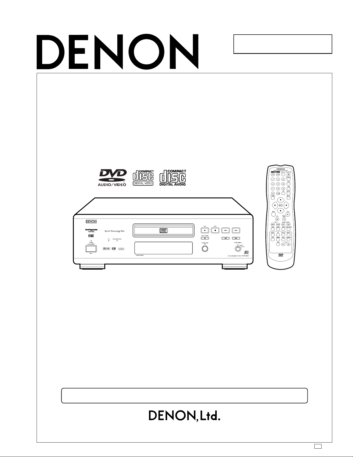
SERVICE MANUAL
For U.S.A., Canada, Europe,
Asia & Korea model
Digital Player
MODEL
DVD AUDIO-VIDEO PLAYER
DVD-3800
Some illustrations using in this service manual are slightly different from the actual set.
16-11, YUSHIMA 3-CHOME, BUNKYOU-KU, TOKYO 113-0034 JAPAN
Telephone: 03 (3837) 5321
X0137 NC 0207

SAFETY PRECAUTIONS
The following check should be performed for the continued protection of the customer and service technician.
LEAKAGE CURRENT CHECK
Before returning the unit to the customer, make sure you make either (1) a leakage current check or (2) a line to chassis
resistance check. If the leakage current exceeds 0.5 milliamps, or if the resistance from chassis to either side of the
power cord is less than 460 kohms, the unit is defective.
SPECIFICATIONS
Signal System: NTSC/PAL
Applicable Discs: (1) DVD-Audio/DVD-Video discs
1-layer 12 cm single-sided discs, 2-layer 12 cm single-sided discs,
2-layer 12 cm double-sided discs (1 layer per side)
1-layer 8 cm single-sided discs, 2-layer 8 cm single-sided discs,
2-layer 8 cm double-sided discs (1 layer per side)
(2) Compact discs (CD-DA, Video CD)
12 cm discs, 8 cm discs
S-Video Output: Y output level: 1 Vp-p (75 Ω/ohms)
C output level: 0.286 Vp-p (For U.S.A., Canada, Asia & Korea model)
Output connectors: S connectors, 2 setS
Video Output: Output level: 1 Vp-p (75 Ω/ohms)
Output connector: Pin-plug jacks, 2 setS
Component Output: Y output level: 1 Vp-p (75 Ω/ohms)
B/CB output level: 0.648 Vp-p (75 Ω/ohms) (For U.S.A., Canada, Asia & Korea model)
P
PR/CR output level: 0.648 Vp-p (75 Ω/ohms) (For U.S.A., Canada, Asia & Korea model)
Output connector: Pin jack, 1 set
RGB Output: Output level: 0.7 Vp-p (75 Ω/ohms) (For Europe model)
Output connector: AV 1 connector, 1 set (For Europe model)
Audio Output: Output level: 2 Vrms
Audio Output Properties: (1) Frequency response
1
DVDs (linear PCM) : 2 Hz to 22 kHz (48 kHz sampling)
2
CDs : 2 Hz to 20 kHz
(2) S/N ratio
1
DVDs : 116 dB
2
CDs : 116 dB
(3) Total harmonic distortion
1
DVDs : 0.0015 %
2
CDs : 0.0018 %
(4) Dynamic range
1
DVDs : 108 dB
2
CDs : 100 dB
Digital Audio Output: Optical digital output : Optical connector, 1 set
Coaxial digital output : Pin jack, 1 set
Power Supply: AC 120 V, 60 Hz (For U.S.A. & Canada model)
AC 230 V, 50 Hz (For Europe & Asia model)
AC 220 V, 50 Hz (For China model)
AC 220 V, 60 Hz (For Korea model)
Power Consumption: 30 W (For U.S.A. & Canada model)
32 W (For Europe, Asia & Korea model)
Maximum External Dimensions: 434 (W) × 132 (H) × 343 (D) mm (including protruding parts)
Mass: 10.0 kg
Remote Control Unit: RC-553
Type: Infrared pulse
Power Supply: DC 3 V, 2 "AA" /R6P batteries
∗ Design and specifications are subject to change without notice in the course of product improvement.
0.3 Vp-p (For Europe model)
AV 1 connector, 1 set (For Europe model)
AV 1 connector, 1 set/AV2 connector, 1 set (For Europe model)
0.7 Vp-p (75 Ω/ohms) (For Europe model)
0.7 Vp-p (75 Ω/ohms) (For Europe model)
2 channel (FL, FR) output connector: Pin jacks, 2 sets
Multi channel (C, SW, SL, SR) output connector: Pin jack, 1 set
AV 1, 1 set/AV 2, 1 set (For Europe model)
: 2 Hz to 44 kHz (96 kHz sampling)
: 2 Hz to 88 kHz (192 kHz sampling)
DVD-3800
2
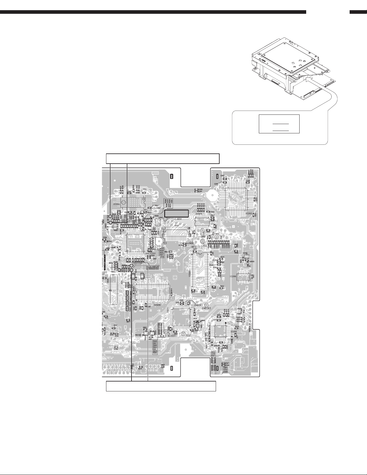
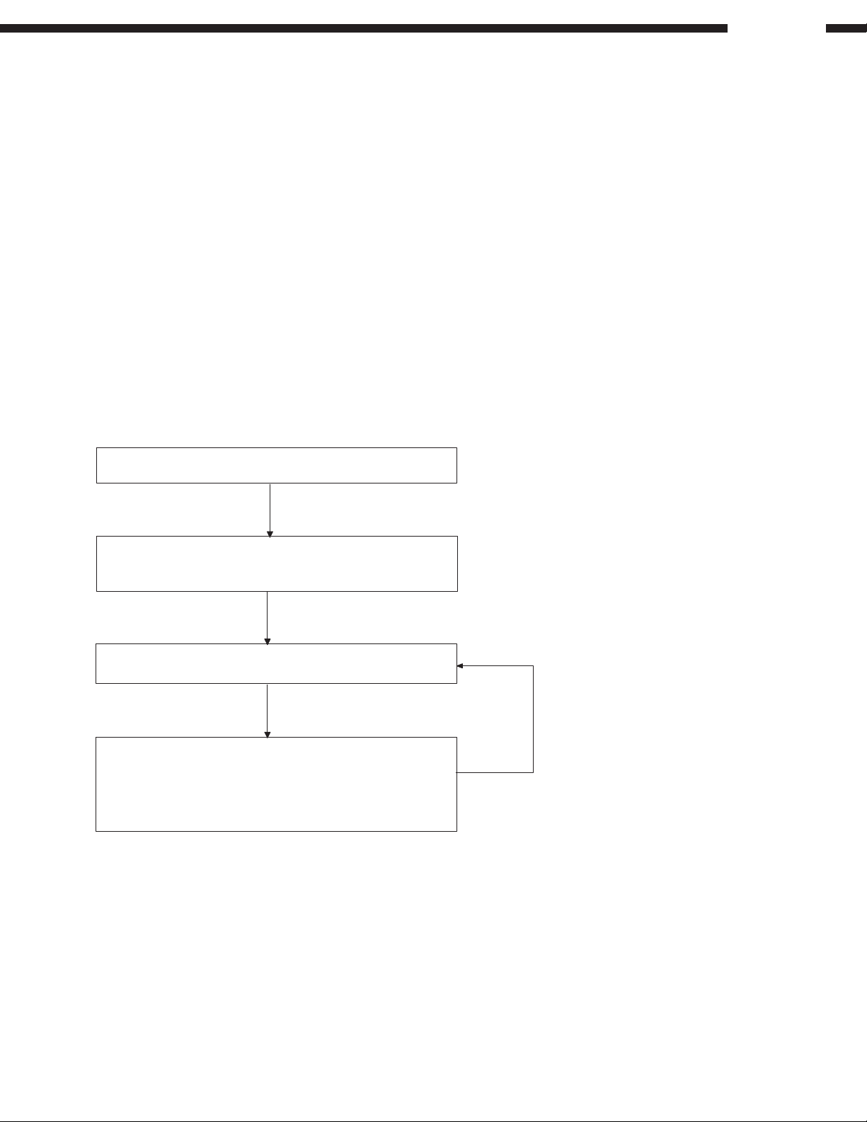
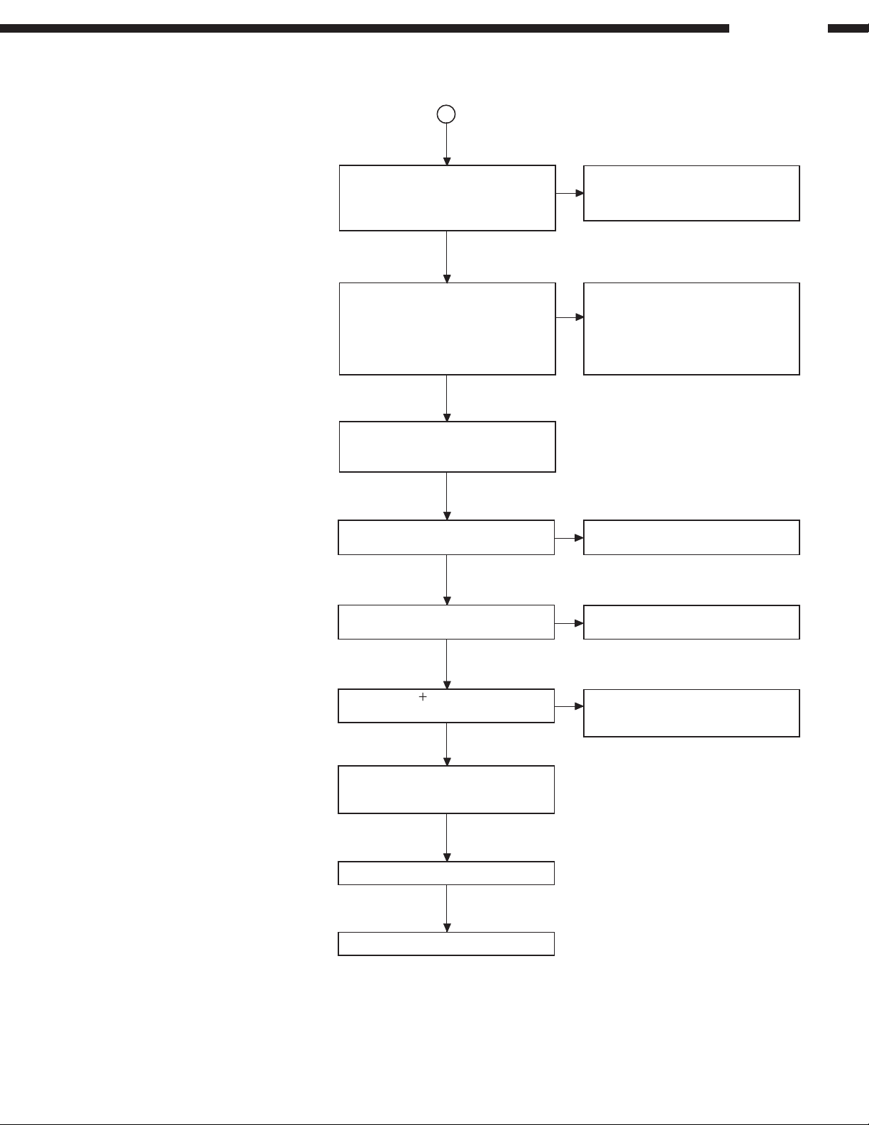
Iop Measurement Method (Diagnostics of Traverse Unit)
Diagnostics of optical pickup (Replacing Traverse Unit) as shown as below.
1. Arrange of Judgment
(1) Check read discs
Disc no read, unsteady playback, etc.
(2) Laser current (Iop) check
Check the Iop (Laser drive current).
If the present Iop value exceeds +50% of the initial value,
replace the Traverse Unit with a new one.
(3) Replacing the Traverse Unit
Traverse Unit replacing (See page 8 and 9).
No mechanical adjustment is necessary after the replacement.
DVD
CD mA
DVD-3800
mA
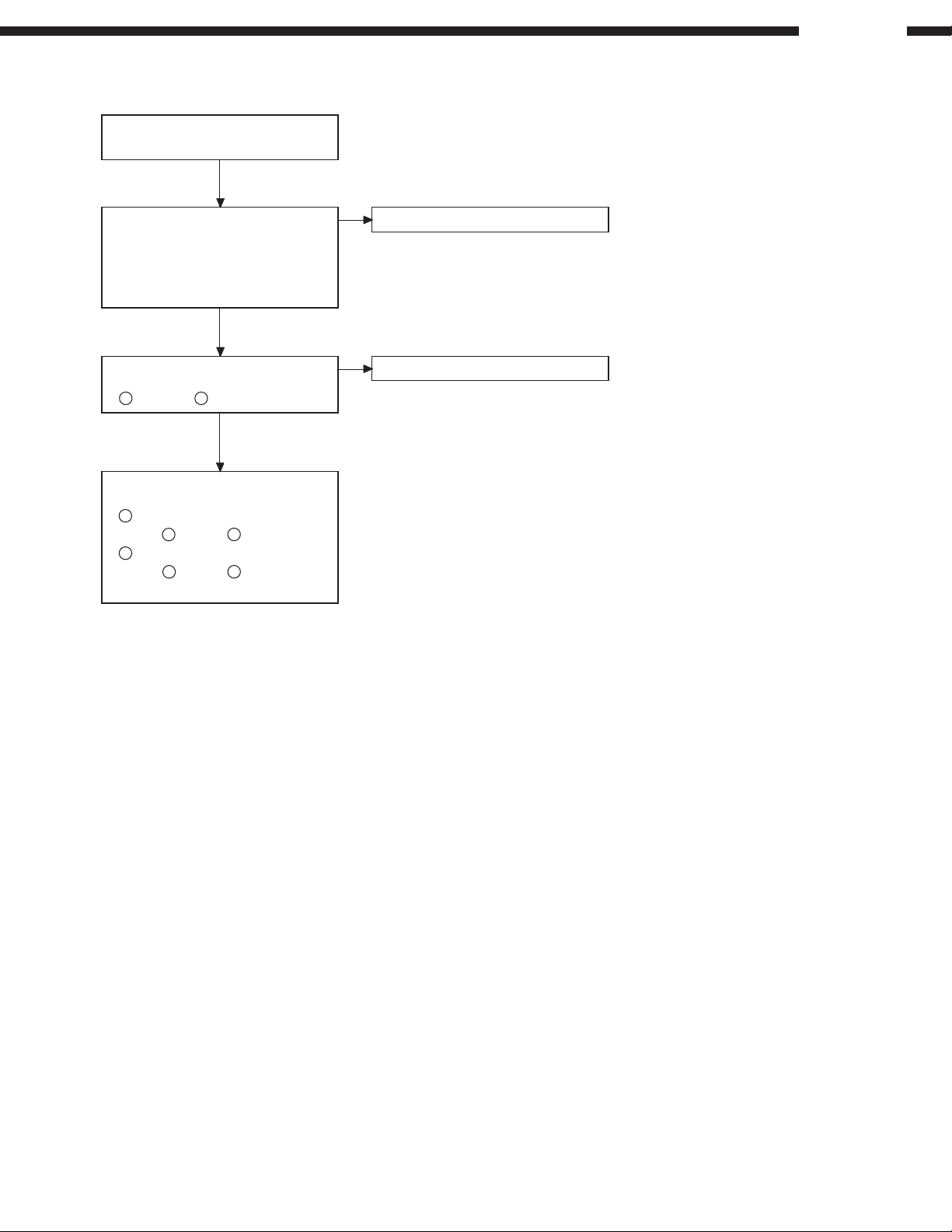
2. Iop Measurement Method
DVD laser drive current measuring points
14
15
60
61
1
4
80
1
Laser current initial value
Nearby C532
29 39
814
7
717
6
1
40
1
1
28
8
1
45
41
40
21
20
2140
1
20
76
1
115
1
20 21
5175
50
18
28
1732
16
40
100
26
1
25
12
24
CD laser drive current measuring points
[CD] IOP silk point
(1) DVD laser current measurement
• Playback the title 1/chapter 1 of DVD test disc (DVDT-S01) or the equivalent.
• Connect the oscilloscope to the above mentioned point.
• DVD laser current = Measured Voltage Value / 39 (Resistance Value)
(2) CD laser current measurement
• Playback the track 1 of CD test disc (TCD-784) or the equivalent.
• Connect the oscilloscope to the above mentioned point.
• CD laser current value = Measured Voltage Value / 39 (Resistance Value)
11
1
48
37
25 36
GU-3389 P.W.B. (foil side)
3
Note for Handling the Laser Pick-up
The protection for the damage of laser diode.
If you want to change the optical device unit from any other units, you must keep the following.
(1) It should be done at the desk already took measures the static electricity in care of removing the OPU's
(Optical device unit) connector cable.
(2) Workers should be put on the "Earth Band".
(3) It shold be done to add the solder to the short land to prevent the broken Laser diode before removing the
24P FFC cable.
(4) Don't touch OPU's connector parts carelessly.
Replacement of the Traverse Unit
When repairing, carry out failure diagnostics by following the procedure described below.
If the present value of the laser drive current is 50% up to initial value, it is the point of the pickup replacement.
In case of the pickup replacement, replace the Traverse Unit with no adjustment.
The initial value is indicated on the label on back side of Mecha.
DVD-3800
NO DISC indicated, Playback not smooth, etc.
Laser drive current check
HF signal check
Present value: 50% up to initial value
Traverse Unit replacement (refer to page 8)
Laser drive current check after replacement.
If the present value is less than 80mA, write on
the new label by hand, put on the new label over
the old label.
If the present value exceeds 80mA,
replace the Traverse Unit with a new one.
Cause: Damaged electrostatically when replaced.
4
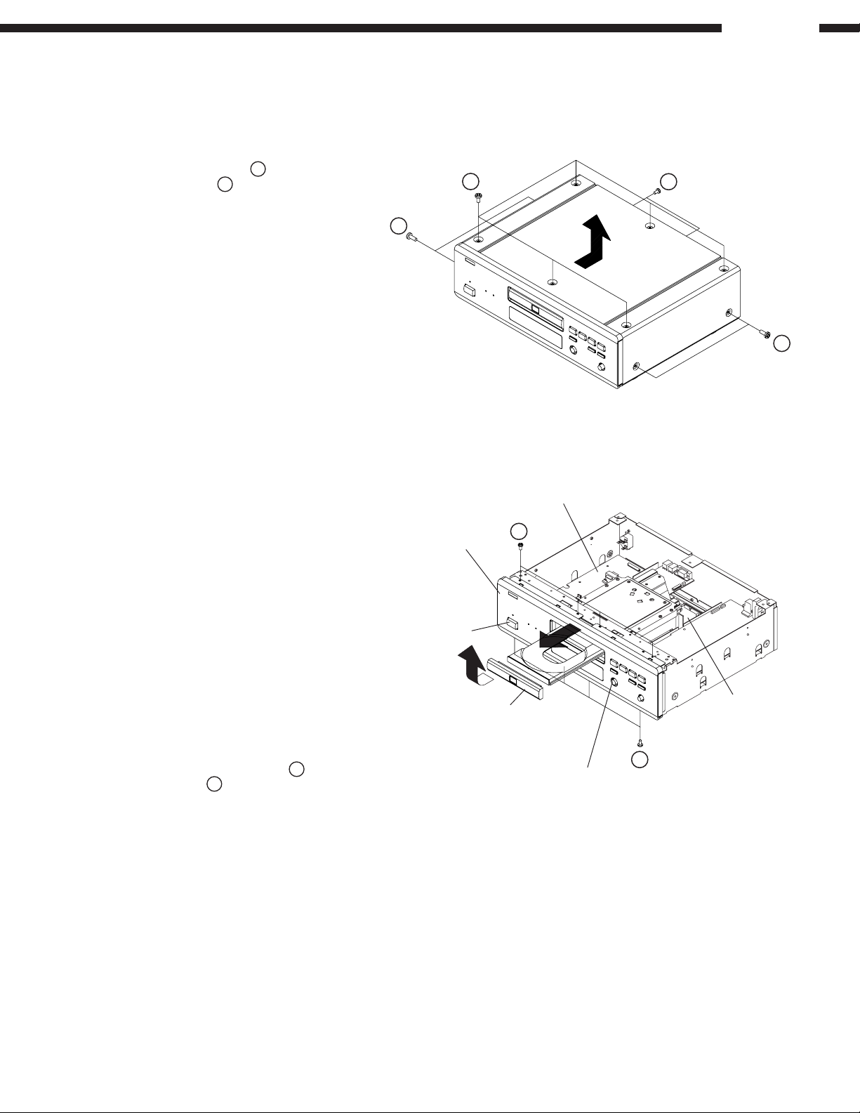
DISASSEMBLY
( Follow the procedure below in reverse order when reassembling )
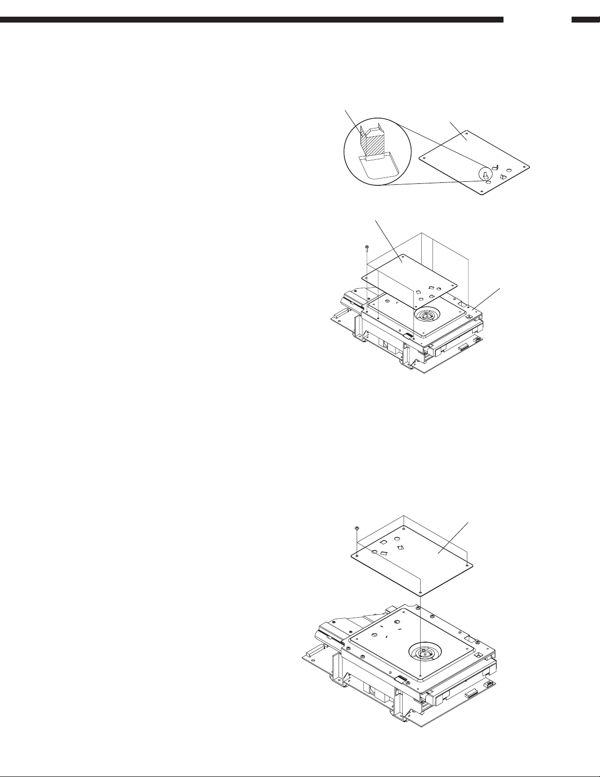
1. Top Cover
(1) Remove 10 screws 1 on the top and both sides,
and 2 screws
(2) Widen the Top Cover a little laterally, then detach it
with sliding in the arrow direction.
on the rear.
2
1
DVD-3800
1
2
1
2. Loader Panel, Front Panel
2-1. When the Disc Tray can be ejected electrically
(1) After removing the Top Cover, proceed
as follows.
(2) Plug the power cord to the wall outlet,
switch on the power, and press the
“OPEN/CLOSE” button to open the Disc
Tray.
(3) Detach the Loader Panel by lifting it in
the arrow direction.
(4) Press the “OPEN/CLOSE” button to
close the Disc Tray, then unplug the
power cord.
(5) Disconnect the wire (CX025, CX041)
connecting the Front Panel’s P.W.B. and
the Power PWB in the Chassis.
3
(6) Remove 4 top screws
4
screws
to the arrow direction.
(7) Disconnect the FFC (CX171) connecting
the Front Panel’s P.W.B. and the Main
P.W.B. in the Chassis.
, then detach the Front Panel
and 4 bottom
Power Switch
Front Panel
Loader Panel
Power P.W.B.
3
Main P.W.B.
4
“OPEN/CLOSE” button
5
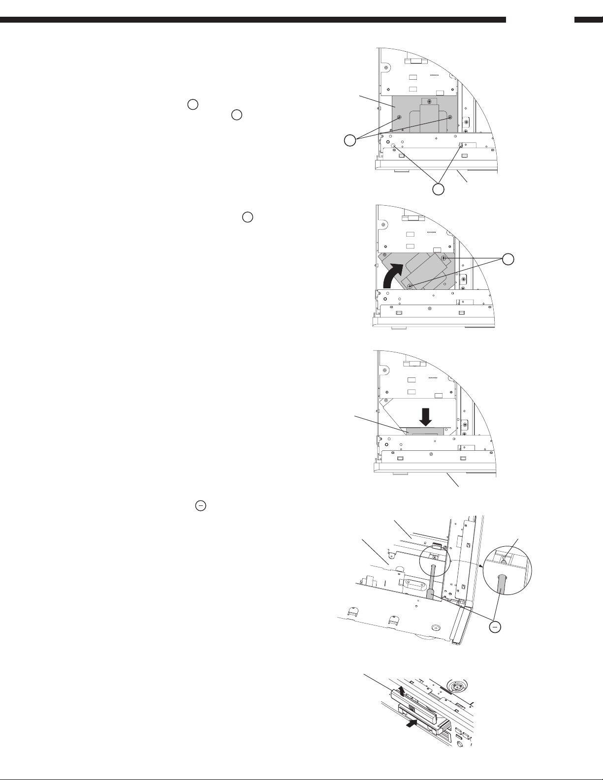
2-2. When the Disc Tray cannot be ejected electrically
(1) After removing the Top Cover, proceed as
follows.
Trans. Bracket
5
(2) Remove 2 screws
Bracket and 2 bottom screws
(3) Turn the Trans. and Bracket to the arrow
direction, then remove 2 screws
on the Trans.
6
.
7
.
DVD-3800
5
Front Panel
6
7
(4) Move the Trans. toward the Front Panel.
(5) Insert a screwdriver
into the left hole of
the Mecha. Fix Bracket, and push the Plate
Gear of the DVD Mecha. slowly to open
the Disc Tray.
Trans.
DVD Mecha.
Mecha. Fix Bracket
Front Panel
Plate Gear
screwdriver
(6) Remove the Loader Panel, and close the
Disc Tray.
(7) Detach the Front Panel following the same
steps described on the previous page 2-1.
(5)~(7).
Loader Panel
6
DVD-3800
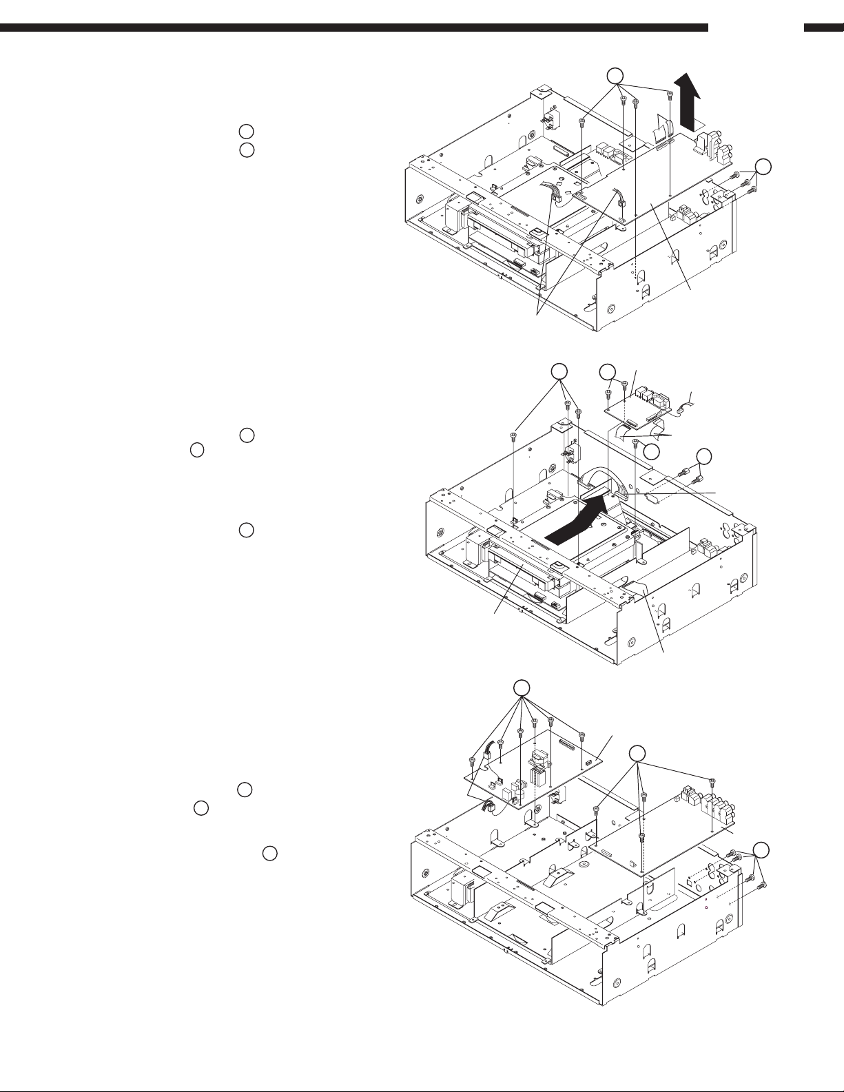
3. Video P.W.B.
(1) Disconnect 2 connectors.
(2) Disconnect 2 FFCs (CY272, CY131).
8
(3) Remove 4 screws
(4) Remove 3 screws
(5) Detach the Video P.W.B. to the arrow direction.
on the Video P.W.B.
9
from the rear.
4. DVD Mecha.
(1) Remove 2 screws on the I/F P.W.B.,
2 screws
2 FFCs (CY211, CY212) and 1 connector
(CY036) to detach the I/F P.W.B.
(2) Disconnect each one of 30P FFC (CY301) and
14P connector (CX141) from the DVD Mecha.
(3) Remove 4 screws
take it off in the arrow direction.
from the rear, then disconnect
on the DVD Mecha., and
Connector
8
I/F P.W.B.
FFC
9
Video P.W.B.
Connector
FFC
14P Connector
5. Audio P.W.B. / Power P.W.B.
5-1. Audio P.W.B.
Remove 4 screw ! on the Audio P.W.B.,
"
4 screws
5-2. Power P.W.B.
(1) Remove 6 screws # on the Power P.W.B.
(2) Disconnect 2 connectors (CX024, CX026).
from the rear.
DVD Mecha.
30P FFC
#
Power P.W.B.
!
Connector
Audio P.W.B.
"
7
A
Solder to short-circuit (CD)
Solder to short-circuit (DVD)
Short-circuit with solder (enlarged fig. A)
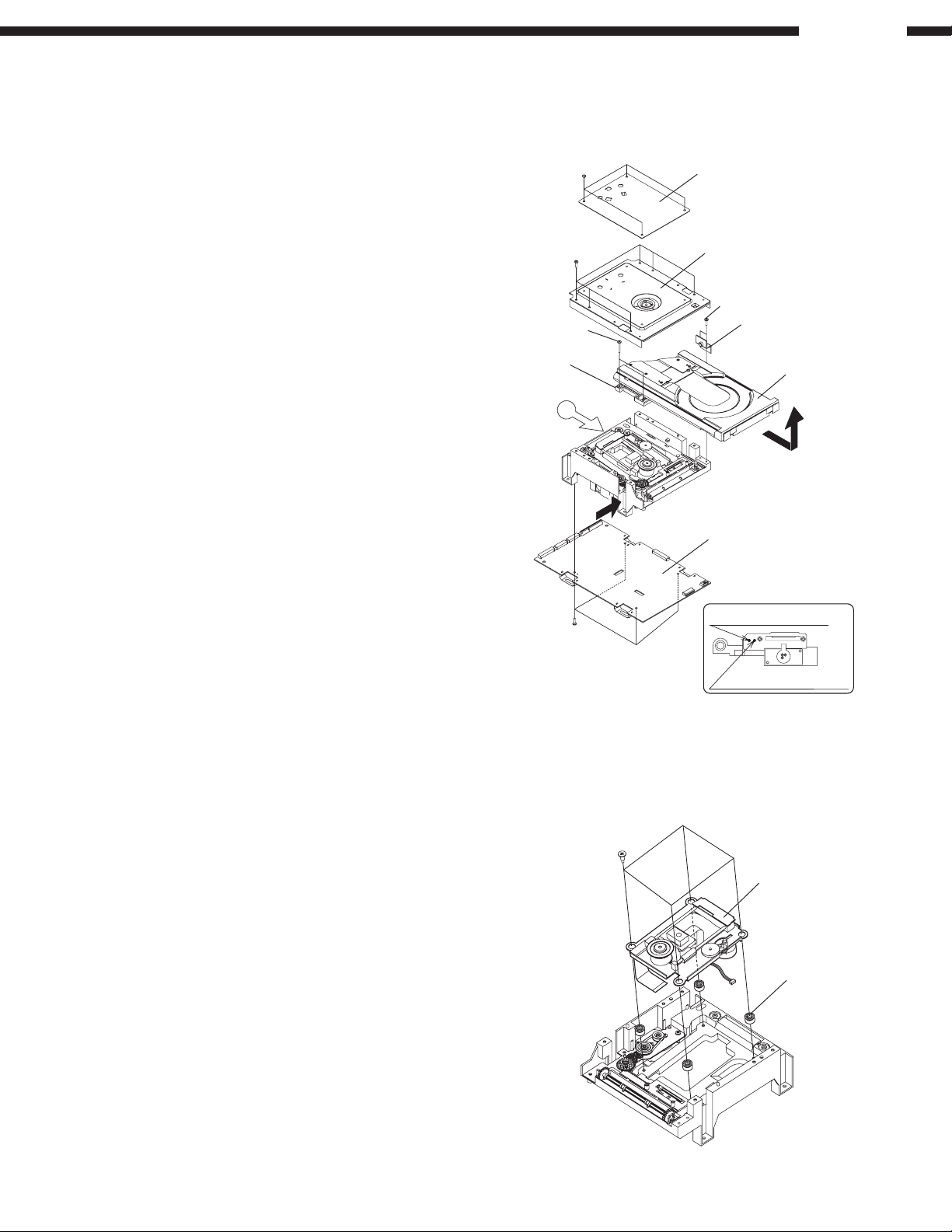
How to Replace Traverse Unit
1. Preparing for Replacement
(1) Removing Clamp Base Damper
Remove 4 pcs of 2.6mm machine screw (a), and detach
the Clamp Base Damper upward.
(2) Removing Clamp Base
Remove 6 pcs of 3mm P-tight screw (b), and detach the
Clamp Base upward.
(3) Ejecting Loader
Through the left rectangular hole of the Mechanism Unit,
push the slider with a ruler or screwdriver until the
Traverse portion lowers and the Loader comes out a little.
(4) Removing Loader
• Remove 2 pcs of 3mm P-tight screw (c) on the Loader
Holder left.
• Remove 2 pcs of 3mm P-tight screw (d) on the Loader
Holder right, then pull up the Bearing Plate.
• Fully pull out the Loader forward, and lift up to take it
out.
(5) Shorting Pickup
To protect the Pickup from static electricity, short-circuit
2 positions as shown in figure.
(6) Removing Main P.W.B. Ass'y
Remove 4 pcs of 3mm P-tight screw (e), and detach the
Main P.W.B. Ass'y downward.
(b)
Holder
(c)
(a)
(3)
DVD-3800
Clamp Base Damper
Clamp Base
(d)
Bearing Plate
Loader
(4)
Main P.W.B. Ass'y
(e)
2. Replacing Traverse Unit
(1) Removing Wires
• CX241: 24P-FFC for Pickup
• CX151: 15P-FFC for Spindle
• CX031: 3P-PH wire for PU Slide
(2) Removing Traverse Unit
Remove 4 pcs of special screw (f) and dampers, then
take out the Traverse Unit upward.
(3) Mounting Traverse Unit
Mount the Traverse Unit following the reverse order.
(f)
Traverse Unit
Damper
8
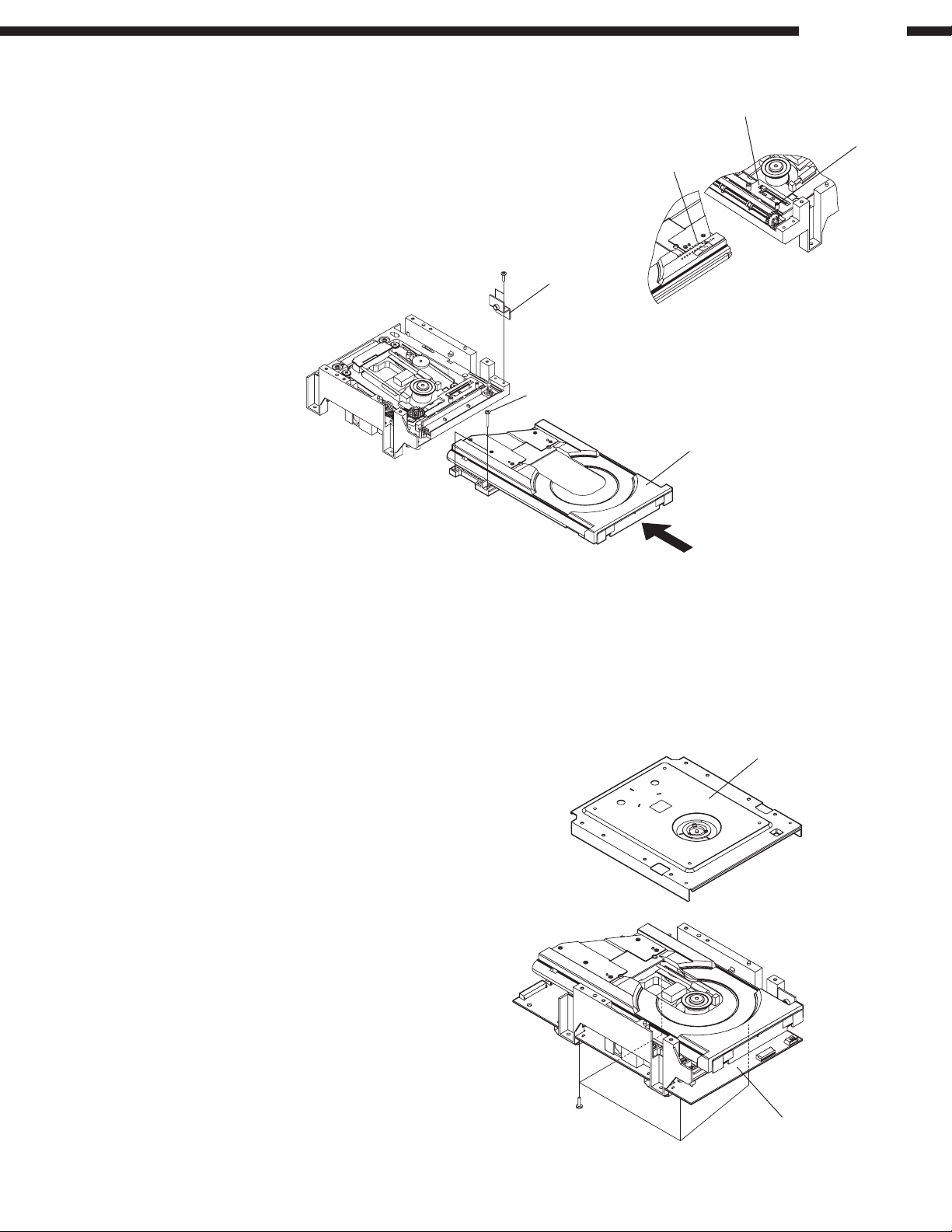
3. Installing Loader
(1) Inserting Loader
Set and push the Loader to the arrow direction until it
stops. When installing the Loader, move the Plate Gear
to right beforehand so as that the boss of the Plate Gear
fits in the backside groove of the Loader. (See figure right)
(2) Fixing Loader
Fix the Loader with each 2 screws (c) and (d).
DVD-3800
Plate Gear
Boss
Groove
(d)
Bearing Plate
(c)
Loader
4. Assembly (1)
(1) Assembling Main P.W.B. Ass'y
Fix the Main P.W.B. Ass'y with 6 pcs of 3mm P-tight
screw (e).
(2) Removing Pickup-short Solder
After connecting 24P-FFC of the Pickup with P.W.B.,
remove solder from 2 shorted positions.
(3) Temporary Positioning Clamp Base
To protect your eyes from laser light, put the Clamp Base
temporarily. (At this moment, be sure to make chucking
the Clamper and Turn-table securly.)
(4) Positioning up Traverse Unit
Connect the following wires of the Mechanism Unit, and
operate it.
• CX141: 14P-PH wire for power
• CX131: 13P-FFC wire from Display P.W.B.
Turn on the power to the unit, and press "OPEN/CLOSE"
button to close the Loader.
The Traverse Unit rises up. (display: 0h00m00s)
Clamp Base
(e)
Main P.W.B. Ass'y
9
5. Assembly (2)
(1) Attaching Tape to Clamp Base Damper
Attach acetate cloth tape to 3 projections of the Clamp
Base Damper backside. (Be careful not to make it
overlapped.)
(2) Assembling Clamp Base
Set the Clamp Base Damper with positioning for clamper
by 3 projections.
Fix the Clamp Base with 6 pcs of 3mm P-tight screw (b).
DVD-3800
Acetate Cloth Tape
Clamp Base Damper
Clamp Base Damper
(b)
Clamp Base
6. Assembly (3)
(1) Detaching Tape from Clamp Base Damper
Detach acetate cloth tape from 3 projections of the Clamp
Base Damper backside.
(2) Assembling Clamp Base Damper
Set the Clamp Base Damper to the Clamp Base contrary
to the direction set in step above.
Fix the Clamp Base Damper with 4 pcs of 3mm S-tight
screw (a).
(a)
Clamp Base Damper
10
DVD-3800
Service Mode
1. Aging Mode
(1) Preparation
(a) Equipment used: Any one of DVD Karaoke Disc (containing more than 10 titles), CD/Video CD (Ver1.0: None
playback control), or No-menu DVD. (Setting varies according to the disc used.)
(b) Unit setting: No spec other than the following procedure (Aging mode)
At the tray open status, press the "POWER" button to turn on the power while pressing the "PLAY" and
"OPEN/CLOSE" buttons for DVD operation simultaneously.
run mode.
(2) Procedure
(a) According the above, set to the aging mode.
(b) Set a DVD Karaoke disc to the tray and press the "PLAY" button once.
(after playback title-1 and title-10 of the disc, the tray open/close is made automatically, then playback the title-1
again) starts. This aging operation continues automatically until it is stopped or it stops caused by an error.
(c) When using other than a DVD Karaoke disc, aging operation (after playback all titles of the disc, the tray open/close
is made automatically, then playback all titles again) starts by pressing the "PLAY" button once, and
the FL lights. The aging operation continues automatically until it is stopped or it stops caused by an error. In case
of some error in DVD, the tray opens and the following error messages are displayed on the FL.
No. Error contents Error code FL display
1 During tray work, it doesn’t end within the time specified. 045300 ERROR 01
2 No spindle work during playback. 040990 ERROR 02
3 Out of focus during playback, search, or pause. 031100 ERROR 04
4 No data read when spin up. 031100 ERROR 04
5 No data read when playback. 031100 ERROR 04
6 Cannot read TOC within the time specified. 025700 ERROR 05
7 No sub-code read 025700 ERROR 05
8 No response from DVD drive more than 10 sec. 0B4000 ERROR 06
9 Error not specified (other than above). --- ERROR 07
mark on the FL lights, and the unit is set to the heat
mark on the FL blinks, and aging peration
mark on
2. Initial Setting Mode
(1) Preparation
(a) Equipment used: None
(b) Unit setting: No spec other than the following procedure
(2) Procedure
(a) Initialize the DVD player when µcom, peripheral parts of µcom, or Main P.W.B. has been replaced in servicing.
(b) Carry out the following to restore factory setting mode. At the player stop condition, press 3 buttons for DVD peration
("PLAY", "OPEN/CLOSE", and "
("Initialized" appears and disappears on the TV screen.)
(c) All user setting will be lost and its factory setting will be restored when this initialization is made. Be sure to
memorize your setting for restoring again after the initialization.
SKIP") until "INITIALIZE" appears and disappears in the FL.
11
3. P.W.B. Check Mode
(1) Preparation
(a) Equipment used: None
(b) Unit setting: No spec other than the following procedure
(2) Procedure
(a) Press the "POWER" button to turn on the power while pressing the "PLAY" and "OPEN/CLOSE" buttons for DVD
operation simultaneously.
(b) FL all light/extinguish mode.
This mode is for detecting FL defects. Press "STILL/PAUSE(
segments, and press it once again to extinguish them.
(c) DVD µcom and main unit µcom firm check mode.
This mode is for displaying the status of each µcom employed.
• DVD µcom firm: Press the "MENU" button. Each time the "MENU" button is pressed, µcom firm is displayed one
after another.
Ex.: [DRV_6067, ESS_6094, PANEL 6093]
Set Serial No. (lower 5 digits) Bus Manager Drive Pcom ESS Pcom Panel Pcom
1 00001~ V.52
2
3
4
Ver. 6067
(Display) 6067
)"on the remote control unit once to light all FL
Ver. 6094
(Display) 6094
Ver. 6093
(Display) 6093
DVD-3800
12
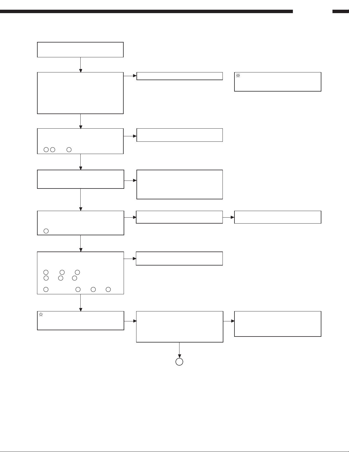
TROUBLESHOOTING
1. No power
(FL tube doesn't light.)
Check connector insertion.
Switching power (GU-3439-1):
[CX024, CX025, CX026, CY041,
CX141]
Main PWB (GU-3389):
[CX031, CX131, CX141, CX171,
CX272]
No
Re-insert the connector. When replacing µcom, µcom
peripheral parts, or Main PWB,
perform initializing of DVD player.
DVD-3800
Check switching power (GU-3439-1)
voltages.
[CX141]: 14P PH for Main PWB:
5
, +5V, "(3.3V)
(1) Check reset signal (3V) at 67pin of
IC601 on DISP PWB.
(2) Check 4.3MHz at 65pin of IC601.
Check switching power (GU-3439-1)
voltages.
[CX041]: 4P PH for Main PWB:
1
+3.6V
Check switching power (GU-3439-1)
voltages.
[CX141]: 14P PH for Main PWB:
1
+12V2-12V3+5V
9
3.3V +5V!+3.3V
[CX041]: 4P PH for DISP PWB:
1
ON/ST(3.6V)2-24V3-29V4-32V
Replace the switching power
No
unit (GU-3439-1).
(1) Check R681, R602 solderring.
No
(2) After checking X601 and IC601
soldering, change X601.
If still NG after changing, replace
IC601.
Check soldering of IC201 on Main PWB
No No
(GU-3389).
Replace the switching power unit
No
(GU-3439-1).
Check after replacing IC201 on Main
PWB (GU-3389).
Perform operation check after
changing Main PWB (GU-3389) with
a perfect one.
There is something wrong in Main PWB
No No
(GU-3389).
→ Check 27MHz output of IC101 (49)
pin/XIN, (105) pin/CLK, and (116) pin/
PCLK2X on Main PWB.
Check soldering of IC108, IC110 and
IC116 on Main PWB (GU-3389), then
change IC101 if it's NG. Change IC111 if
it's still NG.
A
Note: When switching power unit is repairable, refer to the waveforms and voltages shown in Schematic Diagram.
13
DVD-3800
A
There is something wrong in Main PWB
(GU-3389).
→ Check 11MHz input of IC101 (39) pin/
MCLK.
There is something wrong in Main PWB
(GU-3389).
→ Check if CLOCK and DATA signals of
ICBUS are output on IC101 (160) pin/
AUX0, (161) pin/AUX1 when the power
is on.
Check soldering of IC101 (208 pins) on
Main PWB (GU-3389).
→ Perform re-soldering.
Caused by Main PWB (GU-3389).
→Check 20MHz output on IC703(10) pin.
Check IC109→IC113→IC112→IC111
No
(see Schematic Diagram) on Main PWB
(GU-3389).
Check soldering of IC106, IC703, IC706
and IC101 on Main PWB (GU-3389),
No
and change IC101 if it's NG. Change
IC106, then IC703 and IC706 if it's still
NG. Finally, change IC601 on Video
PWB (GU-3438-2) if still NG.
Check soldering of IC703 and X701, and
No
replace if NG.
Caused by Main PWB (GU-3389).
→Check 27MHz input on IC706 (32) pin.
Check RESET 5V output of IC511 (30)
pin on Main PWB.
Check Laser drive current/HF wave form.
Criterion: Iop is less than 1.5 times of its
initial value.
Replace Traverse Unit.
Write Iop after replacing the unit.
Check soldering of IC706, and replace
No
if NG.
Check soldering of R637 and IC101
No
(145) pin on Main PWB.
→ Perform re-soldering.
14
2. No power
(Both FL tube & LED don't light.)
DVD-3800
Check connector insertion.
Switching power (GU-3439-1):
[CX024, CY025, CX028, CY141,
CX041]
Main PWB (GU-3389):
[CX141, CX171]
Check switching power voltages.
[CY141]: 14P PH for Main PWB:
+5V(NSW)"+3.3V(NSW)
Check Main PWB voltages.
[CX171]:
1
pin: +5V check
(CX141 →CX1711 break check)
pin: +3.3V check
(CX141"→CX1712 break check),
etc.
No
Re-insert the connector.
No
Replace the switching power unit.
15
DVD-3800
Electrical Adjustment for Video
SETTING
1. Connect the monitor TV to the video output 1 terminal.
2. Connect the Oscilloscope to the Y-signal and C-signal of S2 video output terminal and each terminate at 75 Ohms.
3. Connect the Oscilloscope to the P
terminate at 75 Ohms.
Use the 75 Ohms resistance must be 1%
4. DVD test disc : DVDT-S01
ADJUSTMENT
Setting the Oscilloscope as bellow.
1
PB / CB / PR / CR
(a) TIME / DIV : 2 µS
(b) VOLT / DIV : 100 mV
(use the probe : ×10)
2
Y / C
(a) TIME / DIV :2 µS
(b) VOLT / DIV :50 mV
(use the probe : ×10)
Power on. Power Supply
U.S.A.& Canada : 120 V
Asia : 230 V
China : 220 V
Europe : 230 V
B-signal , CB-signal and Y-signal of Component video output terminal and each
1. Power on.
2. Set the [SOURCE] selector knob : DVD.
3. Push [OPEN/CLOSE] button, then open the Disc Tray.
4. Set DVD test disc (DVDT-S01) on the Disc Tray, and then push [CLOSE] button.
5. FL display appear "STOP", push [PLAY] button to playback DVD.
6. Set the Video output to INTERLACED by remote control unit. (Push the
[SETUP] button, set to the mode of VIDEO SETUP.)
7. Push the [DISPLAY] button of remote control unit and then appear the ONScreen Display (GUI) on the monitor TV.
8. Push the [12] button, select title 12 of DVD.
9. Push the [SELECT] button, playback title 12. (color bar 75%)
Adjustment Point & Adjustment Value Wave
Adjust the signal of S2 video out by the
wave of Oscilloscope.
1
Y-signal
Adjust the signal of S2 video out by the
wave of Oscilloscope.
2
C-signal
Adjust the signal of Component video out.
1
CB-signal
Point : VR602
Adjustment Value : 1000 ±20 mV
Point : VR603
Adjustment Value : 286 ±5 mV
Point : VR601
Adjustment Value : *525 ±10 mV
Y
Y-signal of S2 video out
C
C-signal of S2 video out
PB
PB-signal
16
Adjustment Point & Adjustment Value Wave
DVD-3800
Adjust the signal of Component video out
2
Y-signal
Set the Video output to PROGRESSIVE by
remote control unit. (Push the [SETUP]
button, set to the mode of VIDEO SETUP.)
1
Y-signal
Set the Video output to PROGRESSIVE by
remote control unit.
(Push the [SETUP] button, set to the mode
of VIDEO SETUP.)
2
PB-signal
Point: VR604
Adjustment Value: 1000 ±20mV
Point: VR710
Adjustment Value: 1000 ±20mV
Point: VR709
Adjustment Value: *525 ±10mV
Y-signal
Y-signal
B-signal
P
Y
Y
PB
Set the Video output to PROGRESSIVE by
remote control unit.
(Push the [SETUP] button, set to the mode
of VIDEO SETUP.)
3
PR-signal
Point: VR708
Adjustment Value: *525 ±10mV
*: 486 ±10mV for U.S.A. & Canada model
R-signal
P
PR
17
DVD DRIVE
MECHA UNIT
[FG-180]
ACT/MOTOR
DRIVER
ATAPI INTERFACE
DVD DECODER
[TC9469BF]
DRIVE CONTROL
µ-COM
[TMP95FY64F]
FRONTEND
PROCESSOR
[TA1293F]
DISC SERVO
PROCESSOR
[TA1293F]
DRAMDRAM
< FRONT END >
DVD PROCESSOR
[ES6038]
64M SDRAM 16M FLASH ROM E2PROM
I/O
EXPAN
PLL
27MHz
OSC
33MHz
OSC
< BACK END >
DIGITAL
POWER
UNIT
64M SDRAM
ANALOG
POWER
UNIT
POWER
TRANS
I/P µCOM
[PIC18LC242]
I/P CONVERTER
[SiI504]
FPGA
XC2530
PROM
VIDEO ENCODER
[ADV7190]
VIDEO ENCODER
[ADV7300]
VR &
FILTER
VR &
FILTER
< VIDEO BLOCK >
MONO MULTI
MONO MULTI
SELECTOR
CLAMP &
DRIVER
CLAMP &
DRIVER
525I/625I
525P
DAC
[PCM1738]
DAC
[PCM1738]
FLASH
ROM
ALPHA
PROCESSOR
[DXP7001]
BASS
MANAGEMENT.
DSP
[ADSPMEL322]
12MHz
OSC
FILTER&
AMP
FILTER&
AMP
FILTER&
AMP
FILTER&
AMP
FILTER&
AMP
FILTER&
AMP
RESET
FLT
KEY ROT SW.REM
WIRED REM
FLASH
ROM
RS-232C
LED
< PANEL CONTROL >
PANEL CONTROL
µ-COM
[MN102H460B]
FL DRIVER
[ML9207]
SPDIF
SW
S L
C
S R
F L
F R
[PCM1738]
DAC
< AUDIO BLOCK >
BLOCK DIAGRAM
DVD-3800
1 5678
32
4
A
B
C
D
E
18
SEMICONDUCTORS
IC’s
Note: Indications before IC numbers denote P.W.B. name.
AV: AUDIO/VIDEO P.W.B.
MA: MAIN P.W.B.
PD: POWER/DISPLAY P.W.B.
SC: SCART P.W.B.
DVD-3800
TC9453F (MA: IC505)
PDON2
132
133
LPFN
134
LPFO
135
PVREF
136
VCOREF
137
VCOF
138
PVDD
139
SLCO1
140
TESM9
141
TEST2
142
RFCD
143
RFDVD
144
AVDD
145
RFCT
146
RFZ1
147
TEZ1
148
AWIN
149
AVSS
150
FE1
151
TE1
152
RFSB
153
RFRP
154
AVSS
155
TESM10
156
EXTAD
157
VREF
158
FOO
159
TRO
160
AVDD
161
AWCTL
162
FMO
163
DMO
164
TEBC
165
FEBC
166
DPDC
167
EQBC
168
ANMON
169
/DFCT
170
VRCK
171
VSS3
172
SCD
173
SCL
174
SCB
175
FGIN
176
NC
PDOP2
131
PDON1
130
PDOP1
129
PESP
128
PVSS
127
from
RF-Amp.
(servo signal)
from
RF-Amp.
(RF signal)
PESV
PPW
CFC2
CFC1
126
125
124
123
VSS3
122
TESM8
121
TESM7
120
TESM6
119
RF Signal
Process
TESM5
PLCK
118
117
ADC
PLL
VDD3NCNC
116
115
114
BD15
113
Sync
BD14
112
111
Digital
Servo
DSP
BD13
VSS5
110
BD12
109
BD11
108
to Driver
Output
DRAM
BD10
BD9
107
106
I/F
ECC
1Mbit
VSS3
105
BD8
104
Analog
Digital
Out
IN
1bit DAC
for CD-DA
Clock
PLL
Output
I/F
MPU I/F
BD7
BD6
BD5
BD4
BD3
BD2
9998979695949392919089
103
102
101
100
BD1
BD0
VDD5
/BWU
Data Out
MPU
/BWL
/BCAS
/BRAS
/BOE
VDD3
BA8
88
BA7
87
BA6
86
BA5
85
BA4
84
VSS5
83
BA3
82
BA2
81
BA1
80
BA0
79
VDD3
78
TESM4
77
DIGI
76
TESM3
75
VDD5
74
PDCK
73
/PDRQ
72
/PSYC
71
PD8
70
PD7
69
PD6
68
PD5
67
VSS3
66
PD4
65
PD3
64
PD2
63
PD1
62
VSS5
61
PD0
60
VDD3
59
VMCK
58
SMCK
57
NC
56
NC
55
VDD5
54
MD7
53
MD6
52
MD5
51
MD4
50
MD3
49
MD2
48
MD1
47
MD0
46
45
/MINT
123456789
NC
NC
LO
RO
DVR
DVSS
DVDD
DVSS
101112131415161718192021222324252627282930313233343536373839404142
XI
XO
XVSS
XVDD
VSS3
VDD3
TESM0
TESM1
TESM2
VSS3
VPFC
MON0
MON1
MON2
MON3
MON4
MON5
VLPF1
VLPF0
TEST0
MON6
NC
NC
VSS3
FLGA
VDD3
MON7
MON8
MON9
FLGB
TEST1
43
44
/MA
/RST
/MCE
/MRD
/MWR
19
TC9453F Terminal Function
DVD-3800
Pin No.
Pin Name Function
1NC
2NC
3DVSS GND for DAC
4 RO O R-ch output signal, Analog output pin
5DVDD Power for DAC
6 DVR O Amp ref. signal output, Analog input pin
7 LO O L-ch output signal, Analog output pin
8DVSS GND for DAC
9XVSS GND for oscillator
10 XI I X’tal osc. input, Analog input pin
11 XO O X’tal osc. output, Analog output pin
12 XVDD Power for oscillator
13 TESM0 Test pin, Connect to GND
14 TESM1 Test pin, Open
15 TESM2 Test pin, Connect to VDD3
16 VDD3 3.3V digital power
17 VSS3 3.3V digital GND
18 VPFC O Clock PLL block phase/freq. comparator out, Analog output pin
19 TEST0 I Test mode pin, Connect to VDD3
20 VLPFI I VCO block filter input for clock PLL, Analog input pin
21 VLPFO O VCO block filter output for clock PLL, Analog output pin
22 VSS3 3.3V digital GND
23 MON0 O Test monitor
24 MON1 O Test monitor
25 MON2 O Test monitor
26 MON3 O Test monitor
27 MON4 O Test monitor
28 MON5 O Test monitor
29 MON6 O Test monitor
30 MON7 O Test monitor
31 MON8 O Test monitor
32 MON9 O Test monitor
33 VDD3 3.3V digital power
34 NC
35 NC
36 TEST1 I Test mode pin, Connect to VDD3
37 FLGA I/O Universal I/O or flag monitor
38 FLGB I/O Universal I/O or flag monitor
39 VSS3 3.3V digital GND
40 /RST I Reset pin, Pull-up resister built-in
41 /MA I µcom address enable signal, Fail-safe pin
42 /MRD I µcom data read signal, Fail-safe pin
43 /MWR I µcom data write signal, Fail-safe pin
44 /MCE I µcom chip enable signal, Fail-safe pin
45 /MINT O µcom interrupt signal, Open drain pin
46 MD0 O µ com data bus
47 MD1 O µ com data bus
48 MD2 O µ com data bus
49 MD3 O µ com data bus
50 MD4 O µ com data bus
51 MD5 O µ com data bus
52 MD6 O µ com data bus
53 MD7 O µ com data bus
54 VDD5 Power for 5V
55 NC
56 NC
57 SMCK O 22M block clock output
58 VMCK O Data output block (signal processing system) clock output
I/O
20
DVD-3800
Pin No.
Pin Name Function
59 VDD3 3.3V digital power
60 PD0 O DVD/CD data output
61 VSS5 GND for 5V
62 PD1 O DVD/CD data output
63 PD2 O DVD/CD data output
64 PD3 O DVD/CD data output
65 PD4 O DVD/CD data output
66 VSS3 3.3V digital GND
67 PD5 O DVD/CD data output
68 PD6 O DVD/CD data output
69 PD7 O DVD/CD data output
70 PD8 O DVD/CD data output
71 /PSYC O DVD data sector sync signal
72 /PDRQ O DVD data transfer block
73 PDCK O DVD data transfer clock
74 VDD5 Power for 5V
75 TESM3 Test pin, Connect to VSS5
76 DIGI I 1bit DAC digital-in input
77 TESM4 Test pin, Connect to VSS5
78 VDD3 3.3V digital power
79 BA0 O External RAM address output
80 BA1 O External RAM address output
81 BA2 O External RAM address output
82 BA3 O External RAM address output
83 VSS5 GND for 5V
84 BA4 O External RAM address output
85 BA5 O External RAM address output
86 BA6 O External RAM address output
87 BA7 O External RAM address output
88 BA8 O External RAM address output
89 VDD3 3.3V digital power
90 /BOE O External RAM/OE signal
91 /BRAS O External RAM/RAS signal
92 /BCAS O External RAM/CAS signal
93 /BWL O External RAM Lower/WE signal
94 /BWU O External RAM Upper/WE signal
95 VDD5 Power for 5V
96 BD0 I/O External RAM data in/output
97 BD1 I/O External RAM data in/output
98 BD2 I/O External RAM data in/output
99 BD3 I/O External RAM data in/output
100 BD4 I/O External RAM data in/output
101 BD5 I/O External RAM data in/output
102 BD6 I/O External RAM data in/output
103 BD7 I/O External RAM data in/output
104 BD8 I/O External RAM data in/output
105 VSS3 3.3V digital GND
106 BD9 I/O External RAM data in/output
107 BD10 I/O External RAM data in/output
108 BD11 I/O External RAM data in/output
109 BD12 I/O External RAM data in/output
110 VSS5 GND for 5V
111 BD13 I/O External RAM data in/output
112 BD14 I/O External RAM data in/output
113 BD15 I/O External RAM data in/output
114 NC
115 NC
116 VDD3 3.3V digital power
117 PLCK I/O PLL block clock in/output
I/O
21

DVD-3800
Pin No.
* Pin names begin with “/” are active “L” terminals.
Pin Name Function
118 TESM5 Test pin, Connect to GND
119 TESM6 Test pin, Connect to GND
120 TESM7 Test pin, Open
121 TESM8 Test pin, Open
122 VSS3 3.3V digital GND
123 CFC1 O VCO frequency control signal, Analog output pin
124 CFC2 O VCO frequency control signal, Analog output pin
125 PPW O Phase comparator offset adj. V out, Analog output pin
126 PESV I Phase comparator offset adj. sig. in, Analog input pin
127 PVSS GND for 3.3V PLL block
128 PESP O Phase comparator offset adj. sig. out, Analog output pin
129 PDOP1 O DVD/CD phase control sig. (positive), Analog output pin
130 PDON1 O DVD/CD phase control sig. (negative), Analog output pin
131 PDOP2 O DVD/CD phase control sig. (positive), Analog output pin
132 PDON2 O DVD/CD phase control sig. (negative), Analog output pin
133 LPFN I Data PLL low pass filter inverted input, Analog input pin
134 LPFO O Data PLL low pass filter output, Analog output pin
135 PVREF Ref. V for data PLL block
136 VCOREF I VCO reference, Analog input pin
137 VCOF I VCO auto-adj. filter out, Analog input pin
138 PVDD Power for 3.3V PLL block
139 SLCO1 O Data slice 6bitDAC out, Analog output pin
140 TESM9 Test pin, Open
141 TEST2 I Test mode pin, Connect to VDD3
142 RFCD I CD RF signal input, Analog input pin
143 RFDVD I DVD RF signal input, Analog input pin
144 AVDD Power for 3.3V analog block
145 RFCT I RFRP center V input (zero-cross intake), Analog input pin
146 RFZI I RFRP signal input (zero-cross intake), Analog input pin
147 TEZI I Tracking error signal input (zero-cross intake), Analog input pin
148 AWIN I Active wide PLL control signal input, Analog input pin
149 AVSS GND for 3.3V analog block
150 FEI I Focus error signal input, Analog input pin
151 TEI I Tracking error signal input, Analog input pin
152 RFSB I RF level or sub beam signal add input, Analog input pin
153 RFRP I RFRP signal input, Analog input pin
154 SAVSS GND for 3.3V analog block
155 TESM10 Test pin, Connect to VREF
156 EXTAD I Universal outside ADC input, Analog input pin
157 VREF Ref. V (1.65V) for analog block
158 FOO O Focus EQ output, Analog output pin
159 TRO O Tracking EQ output, Analog output pin
160 AVDD Power for 3.3V analog block
161 AWCTL O Active wide PLL control output, Analog output pin
162 FMO O Focus EQ output, Analog output pin
163 DMO O Disc EQ output, Analog output pin
164 TEBC O Tracking balance control signal, Analog output pin
165 FEBC O Focus balance control signal, Analog output pin
166 DPDC O DPD error signal pit depth adj. signal, Analog output pin
167 EQBC O RF wide boost adj. signal, Analog output pin
168 ANMON O Universal PWM output, Analog output pin
169 /DFCT O Black dot detect signal
170 VRCK O RF EQ characteristic control clock
171 VSS3 3.3V digital GND
172 SCD O Head amp serial data
173 SCL O Head amp serial data latch pulse
174 SCB O Head amp serial data clock
175 FGIN I Disc FG signal input (w/ self-bias circuit), Feedback R/Analog input pin
176 NC
I/O
22
TC9469BF (MA: IC508)
PSYCN.PDROM
PDCK
PDA8
PDA(7:0)
TEST2-0
/RST
DVD-3800
Buffer
DRAM 256kw/128kw/64kw
tion
Correc-
9
AUTH
CD-IF &
DVD-IF
SUB-IF
(4Mbit/2Mbit/1Mbit)
Da
Daf
HEDda
HSYC
SBDa
SBQa
BSYC
M-FIFO
´
3ch)
(8B
MD7-0
SEDVD
3
Input
Selecter
Input
8
IF
Convert
Gnd
Vdd
30
Clock
3
XI
XO
BD15-0
/BWU./BWL
/RAS./CAS
/BOE
BA8-0
3
16
64
16
8
64
16
16
8
(M-IF)
M Interrupt
M Address
7
3
8
/MCE
MA6-0
/MWR./WRD
2
9
Buffer
Address
16
ECC
8
8
/MINT
(H-IF)
H-FIFO
(64B)
64
H Interrupt
8
16
AV-IF
ASYC
TC9469BF
m com
CSEL
/PDIAG./DASP
2
IORDY
HDRQ
/HDAK
/IOCS16
16
HD15-0
2
/HRD./HWR
Driver
5
/HCS3./HCS1
HA2-0
INTRQ
DIGO
AZCK
3
ABCK.ACHCK
ADO
V
HD7
HD8
HD6
HD9
HD5
HD10
V
HD4
HD11
HD3
HD12
HD2
HD13
HD1
HD14
HD0
V
V
HD15
HDRQ
/HWR
VSShr
/HRD
V
SS
IORDY
V
DD
V
/HDAK
INTRO
/IOCS16
HA1
/PDIAG
HA0
V
(NC)
SSVSSVDD
/RST
ESTOUT
/MINT
/MWR
VSS/WRD
/WCE
MA6
MA5
MA4
MA3
MA2
MA1
MA0
VDDVSSMD7
MD6
MD5
MD4
MD3
MD2
MD1
MD0
VSSSEDVD
VDDACHCK
AD0
ABCK
AZCK
(NC)
V
108
107
106
105
104
103
109
DD
999897969594939291908988878685848382818079787776757473
102
101
100
110
111
112
113
114
115
SS
116
117
118
119
120
121
122
123
124
125
126
DD
127
SS
128
129
130
131
132
133
24
134
135
24
136
SS
137
138
139
140
141
142
143
DD
144
(NC)
(NC)
72
(NC)
71
V
70
SS
69
(LRCK)PDA0
(BCK)PDA1
68
(DA1)PDA2
67
(C2P1)PDA3
66
(CLCK)PDA4
65
V
64
SS
63
(SB01)PDA5
(SFSY)PDA6
62
(SBSY)PDA7
61
PDA8
60
PSYCN
59
PDRQN
58
PDCK
57
(NC)
56
DIGO
55
VDDck
54
X0
53
X1
52
VSSck
51
TEST2
50
TEST1
49
TEST0
48
BA3
47
BA1
46
BA2
45
V
44
SS
43
BA0
BA4
42
BA5
41
BA6
40
BA7
39
V
38
SS
37
(NC)
123456789
(NC)
SS
A2
V
/HCS1
SS
V
CSEL
/HCS3
/DASP
101112131415161718192021222324252627282930313233343536
DD
V
BD15
BD14
BD13
BD12
BD11
BD10
SS
DD
V
V
BD4
BD5
BD7
BD6
BD9
BD8
BD3
SS
V
BD2
BD1
BD0
/RAS
/BOE
/BWU(/BWE)
/BWL(/CASL)
/CAS(/CASU)
DD
V
BA8
(NC)
23

TC9469BF Terminal Function
DVD-3800
Pin No.
Pin Name Function
1NC
2VSS GND pin
3 HA2 I Host address 2 input: IDE sig. DA2, TTL level input, pull-up R built-in
4 /HCS1 I Chip select 1 input: IDE sig. /CS1FX, TTL level input, pull-up R built-in
5 HCS3 I Chip select 3 input: IDE sig. /CS3FX, TTL level input, pull-up R built-in
6 /DASP I/O Drive active in/output: IDE sig. /DASP, TTL level input, open drain out, pull-up R built-in
7 CSEL I Cable select pin: IDE sig. CSEL
8VSS GND pin
9VDD Power pin
10 BD15 I/O Buffer RAM data in/output, at low power: output
11 BD14 I/O Buffer RAM data in/output, at low power: output
12 BD13 I/O Buffer RAM data in/output, at low power: output
13 BD12 I/O Buffer RAM data in/output, at low power: output
14 BD11 I/O Buffer RAM data in/output, at low power: output
15 BD10 I/O Buffer RAM data in/output, at low power: output
16 BD9 I/O Buffer RAM data in/output, at low power: output
17 BD8 I/O Buffer RAM data in/output, at low power: output
18 VDD Power pin
19 VSS GND pin
20 BD4 I/O Buffer RAM data in/output, at low power: output
21 BD5 I/O Buffer RAM data in/output, at low power: output
22 BD7 I/O Buffer RAM data in/output, at low power: output
23 BD6 I/O Buffer RAM data in/output, at low power: output
24 BD3 I/O Buffer RAM data in/output, at low power: output
25 BD2 I/O Buffer RAM data in/output, at low power: output
26 BD1 I/O Buffer RAM data in/output, at low power: output
27 BD0 I/O Buffer RAM data in/output, at low power: output
28 VSS GND pin
29 /BWU O For write enable bit (for /BWE sig.), at low power: H
30 /BWL O For /CAS signal lower 8bit (for /CASL sig.), at low power: H
31 /CAS O For /CAS signal upper 8bit (for /CASU sig.), at low power: H
32 /RAS O RAS signal output, at low power: H
33 /BOE O Output enable, at low power: H
34 BA8 O Buffer address output
35 VDD Power pin
36 NC
37 NC
38 VSS GND pin
39 BA7 O Buffer address output
40 BA6 O Buffer address output
41 BA5 O Buffer address output
42 BA4 O Buffer address output
43 BA0 O Buffer address output
44 VSS GND pin
45 BA2 O GND pin
46 BA1 O GND pin
47 BA3 O Buffer address output
48 TEST0 I Test pin, Fixed to “L”
49 TEST1 I Test pin, Fixed to “L”
50 TEST2 I Test pin, Fixed to “L”
51 VSSck GND pin (for clock system)
52 XI I Master clock in/output, feedback R built-in
53 XO O Master clock in/output, feedback R built-in
54 VDDck Power pin (for clock system)
55 DIGO O Digital out pin
56 NC
57 PDCK I Data read clock input
58 PDRQN I Data effective flag input
I/O
24
DVD-3800
Pin No.
Pin Name Function
59 PSYCN I Sync signal input
60 PDA8 I Parallel data 8 input
61 PDA7 I Parallel data 7 input
62 PDA6 I Parallel data 6 input
63 PDA5 I Parallel data 5 input
64 VSS GND pin
65 PDA4 I Parallel data 4 input
66 PDA3 I Parallel data 3 input
67 PDA2 I Parallel data 2 input
68 PDA1 I Parallel data 1 input
69 PDA0 I Parallel data 0 input
70 VSS GND pin
71 NC
72 NC
73 NC
74 AZCK I Ref. clock input for audio playback
75 ABCK O Bit clock (BCK) output for audio playback
76 ADO O Data output for audio playback
77 ACHCK O Channel clock (LRCK) output for audio playback
78 VDD Power pin
79 SEDVD I Input IF select
80 VSS GND pin
81 MD0 I/O µcom data in/output, tri-state output
82 MD1 I/O µcom data in/output, tri-state output
83 MD2 I/O µcom data in/output, tri-state output
84 MD3 I/O µcom data in/output, tri-state output
85 MD4 I/O µcom data in/output, tri-state output
86 MD5 I/O µcom data in/output, tri-state output
87 MD6 I/O µcom data in/output, tri-state output
88 MD7 I/O µcom data in/output, tri-state output
89 VSS GND pin
90 VDD Power pin
91 MA0 I µcom address input
92 MA1 I µcom address input
93 MA2 I µcom address input
94 MA3 I µcom address input
95 MA4 I µcom address input
96 MA5 I µcom address input
97 MA6 I µcom address input
98 /MCE I Chip enable signal input
99 /MRD µcom chip read signal input
100 VSS GND pin
101 /MWR I µcom write signal input
102 /MINT O µcom interrupt signal output, open drain, pull-up R built-in
103 TESTOUT O Output for test, leave it open
104 /RST I Hardware reset input (CMOS level), pull-up R built-in
105 VDD Power pin
106 VSS GND pin
107 VSS GND pin
108 NC
109 VDD Power pin
110 HD7 I/O
111 HD8 I/O
112 HD6 I/O
113 HD9 I/O Host data in/output (HD[0:15]:IDE sig. DD[0:15]), TTL level, tri-state out, pull-up R built-in
114 HD5 I/O
115 HD10 I/O
116 VSS GND pin
I/O
25
DVD-3800
Pin No.
Pin Name Function
I/O
117 HD4 I/O
118 HD11 I/O
119 HD3 I/O
120 HD12 I/O
121 HD2 I/O Host data in/output (HD[0:15]:IDE sig. DD[0:15]), TTL level, tri-state out, pull-up R built-in
122 HD13 I/O
123 HD1 I/O
124 HD14 I/O
125 HD0 I/O
126 VDD Power pin
127 VSS GND pin
128 HD15 I/O Host data in/output (HD[0:15]:IDE sig. DD[0:15])
129 HDRQ O Data request output: IDE sig. DMARQ, tri-state out, drive-ability 12mA
130 /HWR I Host write signal input: IDE sig. /DIOW, TTL level, pull-up R built-in
131 VSShr GND pin (for /HR)
132 /HRD I Host read signal input: IDE sig. /DIOR, TTL level, pull-up R built-in
133 VSS24 GND pin (for IORDY)
134 IORDY O IO transfer ready output: IDE sig. IORDY, tri-state out, drive-ability 24mA
135 VDD24 Power pin (for IORDY)
136 VSS GND pin
137 /HDAK I Data acknowledge input: IDE sig. /DMACK, TTL level, pull-up R built-in
138 INTRQ O Interrupt signal output: IDE sig. INTRQ, tri-state out, drive-ability 12mA
139 /IOCS16 O Data bit wide select output: IDE sig. /IOCS16, open drain, pull-up R built-in
140 HA1 I Host address 1 input: IDE sig. DA1, TTL level, pull-up R built-in
141 /PDIAG I/O Post diagnostic in/output: IDE sig. /PDIAG, TTL level, tri-state out, pull-up R built-in
142 HA0 I Host address 0 input: IDE sig. DA0, TTL level, pull-up R built-in
143 VDD Power pin
144 NC
* Pin names begin with “/” PSYNCN, and PDRQN are active “L” terminals.
MX29LV160BTC-90 (MA: IC102)
1
A15
2
A14
3
A13
4
A12
5
A11
6
A10
7
A9
A8
8
A19
9
NC
10
11
WE
RESET
12
NC
13
14
NC
RY/BY
15
A18
16
17
A17
A7
18
19
A6
20
A5
21
A4
22
A3
23
A2
24
A1
48
47
46
45
44
43
42
41
40
39
38
37
36
35
34
33
32
31
30
29
28
27
26
25
SYMBOL PIN NAME
A16
BYTE
A0~A19 Address Input
GND
Q0~Q14 Data Input/Output
Q15/A-1
Q15/A-1 Q15 (Word mode)/LSB addr (Byte mode)
Q7
Q14
CE Chip Enable Input
Q6
WE Write Enable Input
Q13
BYTE Word/Byte Selection input
Q5
RESET Hardware Reset Pin/Sector Protect Unlock
Q12
Q4
OE Output Enable Input
V
CC
RY/BY Ready/Busy Output
Q11
VCC Power Supply Pin (2.7V~3.6V)
Q3
Q10
GND Ground Pin
Q2
Q9
Q1
Q8
Q0
OE
GND
CE
A0
26
TMP95FY64F (MA: IC511)
DVD-3800
100
76
77
78
79
80
81
82
83
84
85
86
87
88
89
90
91
92
93
94
95
96
97
98
99
P33/A11
P32/A10
P31/A9
P30/A8
P47/A7
P46/A6
P45/A5
P44/A4
P43/A3
P42/A2
P41/A1
P40/A0
P50/RD
P51/WR
P52/HWR
(GND)VSS
PA0/AN0
PA1/AN1
PA2/AN2
PA3/AN3/ADTRG
PA4/AN4
PA5/AN5
PA6/AN6
PA7/AN7
VREFH
TMP95FY64F Terminal Function
P34/A12
P35/A13
P36/A14
P37/A15
P20/A16
P21/A17
P22/A18
P23/A19
P24/A20
P25/A21
757473727170696867666564636261605958575655
123456789
AVSS
AVCC
VREFL
DAOUT0
NMI
DAOUT1
P53/BUSRQ
P55/WAIT
P54/BUSAK
1011121314
P56/INTO
P26/A22
P57/SCLK2/CTS2
P27/A23
P80/TxD0
P17/D15
VCC
VSS(GND)
AM8/16
15161718192021
P83/TxD1
P84/RxD1
P81/RxD1
P82/SCLK0/CTS0
P16/D14
P85/SCLK1/CTS1
P15/D13
P86/TxD2
P14/D12
P87/RxD2
P13/D11
P60/CS0
P12/D10
P11/D9
545352
222324
P61CS1
P62/CS2
P10/D8
P62/CS3
P07/D7
P06/D6
51
P05/D5
50
P04/D4
49
48
P03/D3
P02/D2
47
46
P01/D1
45
P00/D0
44
VCC
P96/TOA/TOB
43
42
P95/TIB/INT8
P94/TIA/INT7
41
P93/TO9
40
39
P92/TO8
P91/TI9/INT6
38
37
P90/TI8/INT5
P75/TO7/INT4
36
P74/TO5
35
P73/TI4/INT3
34
P72/TO3/INT2
33
P71/TO1
32
P70/TI0/INT1
31
RESET
30
EA
29
X2
28
27
X1
26
VSS(GND)
25
CLK
VCC
Pin No.
Pin Name Function
Symbol
I/O
1 VREFL VREFL I Ref. V input (L) for A/D converter
2AVSS AV SS GND
3AVCC AVCC Power
4 DAOUT0 DAOUT0 O D/A output 0
5 DAOUT1 DAOUT1 O D/A output 1
6 NMI NMI I Non-maskable interrupt request pin
7 P53 STBN O TA8493F/BA5952FP standby pin
8 P54 AMUTE O Not used
9 P55 Not used
10 INT0 DSPINT I Interrupt input from TC9453F
11 P57 RSTN O Reset output of TC9453F
12 P80 Not used
13 P81 Not used
14 P82 TEST I Not used
15 P83 Not used
16 P84 TMM+ O Loading motor control pin
17 P85 TMM- O Loading motor control pin
18 P86 O Not used
19 P87 I Not used
20 CS0 DECCSN O TC9469BF chip select
21 CS1 DSPCSN O TC9453F chip select
22 P62 Not used
23 P63 Not used
24 CLK Not used
25 VCC VCC Power
26 VSS VSS GND
27 X1 X1 I X’tal connection
28 X2 X2 O X’tal connection
29 EA EA I Power
30 RESET RESET I Reset input pin
31 INT1 DECINT I Interrupt input from TC9469BF
32 P71 Not used
33 P72 Not used
27
DVD-3800
Pin No.
Pin Name Function
34 INT3 FG I FG signal input from TA8493F
35 P74 BRKN O Brake signal output to TA8493F
36 P75 Not used
37 INT5 SLIDE_PULSE I Pulse counter input of slide
38 P91 P-LOW O PLL filter switching output
39 P92 PLLD Not used
40 P93 P-HIGH O PLL filter switching output
41 INT7 Not used
42 P95 Not used
43 P96 PLLB Not used
44 VCC VCC Power
45 D0 MD0 I/O Data bus
46 D1 MD1 I/O Data bus
47 D2 MD2 I/O Data bus
48 D3 MD3 I/O Data bus
49 D4 MD4 I/O Data bus
50 D5 MD5 I/O Data bus
51 D6 MD6 I/O Data bus
52 D7 MD7 I/O Data bus
53 D8 T22 Not used
54 D9 T9 Not used
55 D10 T10 Not used
56 D11 T11 Not used
57 D12 T12 Not used
58 D13 T13 Not used
59 D14 T14 Not used
60 D15 T15 Not used
61 AM8/16 AM8/16 I Pull-up
62 VSS VSS GND
63 VCC VCC Power
64 P27 BUSY O Busy output
65 P26 O Not used
66 P25 O Not used
67 P24 Not used
68 P23 Not used
69 P22 Not used
70 P21 Not used
71 A16 Not used
72 A15 Not used
73 A14 Not used
74 A13 Not used
75 A12 Not used
76 A11 Not used
77 A10 Not used
78 A9 Not used
79 A8 MA8 O Address bus
80 A7 Not used
81 A6 MA6 O Address bus
82 A5 MA5 O Address bus
83 A4 MA4 O Address bus
84 A3 MA3 O Address bus
85 A2 MA2 O Address bus
86 A1 MA1 O Address bus
87 A0 MA0 O Address bus
88 RD RDN O Strobe signal output for read
89 WR WRN O Strobe signal output for write
90 P52 Not used
91 VSS VSS Powe r
92 PA0 MASTER I Pull-down
93 PA1 SLAVE I Pull-up
94 PA2 CSEL I Pull-up
95 PA3 CLOS I Loader close SW input pin
96 PA4 OPEN I Loader open SW input pin
97 PA5 INSWN I Pickup inner SW input pin
98 AN6 +1.65V I Analog input pin
99 PA7 EJECT I Not used
100 VREFH VREFH I Ref. V input (H) for A/D converter
Symbol
I/O
28
TA1293F (MA: IC501)
LDO1
MDI1
EQF
EQB
RFDC
GND2
EQDNCVcc2
60595857565554535251504948474645444342
VccO
PSC
FEB
TEB
DPDB
VccR
RFO
RPP
RPB
RPO
DVD-3800
RPZ
41
61
P1TN
62
P1TP
P1FN
63
P1FP
64
LDP1
65
GNDR
66
P1DI
67
P1CI
68
P1BI
69
P1AI
70
LDP2
71
P2AI
72
P2BI
73
P2CI
74
P2DI
75
GNDS
76
P2FP
77
P2FN
78
P2TP
79
P2TN
80
123456789
NC
NC
VrA
MDI2
LDO2
GNDP
TA1293F Terminal Function
Pin Name FunctionPin No. I/O
1 GNDP GND pin
2 LDO2 O Drive pin
3 MDI2 I Monitor pin
4 NC Used connecting with VrA
5 NC Used connecting with VrA
6 VrA O Analog VREF
7 Vrfi Filter capacity for reference
8 VrD O Digital VREF, outputs 1/2 of Vdd
9 Vdd I Power pin, connect Vdd of servo IC
10 DPAC DPD AC coupling capacity 1
11 DPBD DPD AC coupling capacity 2
12 DPD1 DPD integral capacity 1
13 DPD2 DPD integral capacity 2
14 SCB I Control line (bit clock)
15 SCL I Control line (latch signal)
16 SCD I Control line (serial data)
17 VRCK I Ref. clock input
18 NC Used connecting with GND
19 NC Used connecting with GND
20 VCKF Capacity for adjusting time constant
21 VccP Power pin
22 NC Used in open
23 NC Used in open
24 NC Used in open
25 NC Used connecting with GND
26 RFSW I RFO control pin, outputs signal after EQ at L
27 VccS Power pin
28 NC Used in open
29 NC Used connecting with VrA
1011121314151617181920
Vrfi
VrD
Vdd
DPAC
DPD1
DPBD
SCB
DPD2
SCL
SCD
NC
VRCK
NC
VCKF
40
39
38
37
36
35
34
33
32
31
30
29
28
27
26
25
24
23
22
21
DFTN
NC
NC
NC
NC
NC
FEO
TEO
NC
LVL
NC
NC
NC
VccS
RFSW
NC
NC
NC
NC
VccP
29
DVD-3800
Pin No.
Pin Name Function
30 NC Used connecting with VrA
31 LVL O Servo addition output
32 NC Used in open
33 TEO O TE output
34 FEO O TE output
35 NC Used connecting with VrA
36 NC Used connecting with VrA
37 NC Used connecting with VrA
38 NC Used connecting with VrA
39 NC Used connecting with VrA
40 DFTN I DPD defect, L: DPD out = Mute
41 RPZ O RF ripple center output
42 RPO O RF ripple output
43 RPB O Bottom of RF ripple
44 RPP O Peak of RF ripple
45 RFO O Equivalent RF output
46 VccR Power pin (RF)
47 DPDB I Pit depth adjustment
48 TEB I TE balance
49 FEB I FE balance
50 PSC I VRCK divide on/off, H: divide off
51 VccO Power pin
52 Vcc2 Power pin
53 NC Connect with VrD, or GND via C
54 EQD I Group delay correction
55 GND2 GND pin
56 RFDC DC feedback capacity
57 EQB I Boost adjustment
58 EQF I Frequency adjustment
59 MDI1 I Monitor input
60 LDO1 O Drive output
61 P1TN I TE(-) input (DVD)
62 P1TP I TE(+) input (DVD)
63 P1FN I FE(-) input (DVD)
64 P1FP I FE(+) input (DVD)
65 LDP1 I APC polarity 1, positive when connected to Vcc
66 GNDR GND pin
67 P1DI I D input (DVD)
68 P1CI I C input (DVD)
69 P1BI I B input (DVD)
70 P1AI I A input (DVD)
71 LDP2 I APC polarity 2, positive when connected to Vcc
72 P2AI I A input (CD)
73 P2BI I B input (CD)
74 P2CI I C input (CD)
75 P2DI I D input (CD)
76 GNDS GND pin
77 P2FP I FE(+) input (CD)
78 P2FN I FE(-) input (CD)
79 P2TP I TE(+) input (CD)
80 P2TN I TE(-) input (CD)
I/O
30