

Denon DVD-310 Service Manual
For Japan model
SERVICE MANUAL
MODEL
DVD VIDEO PLAYER
Ver. 1
DVD-310
注 意
For purposes of improvement, specifications and
●
design are subject to change without notice.
Please use this service manual with referring to
●
the operating instructions without fail.
●
Some illustrations using in this service manual are
slightly different from the actual set.
16-11, YUSHIMA 3-CHOME, BUNKYOU-KU, TOKYO 113-0034 JAPAN
サービスをおこなう前に、このサービスマニュアルを
必ずお読みください。本機は、火災、感電、けがなど
に対する安全性を確保するために、さまざまな配慮を
おこなっており、また法的には「電気用品安全法」に
もとづき、所定の許可を得て製造されております。
従ってサービスをおこなう際は、これらの安全性が維
持されるよう、このサービスマニュアルに記載されて
いる注意事項を必ずお守りください。
● 本機の仕様は性能改良のため、予告なく変更すること
があります。
● 補修用性能部品の保有期間は、製造打切後
修理の際は、必ず取扱説明書を参照の上、作業を行って,
●
ください。
● 本文中に使用しているイラストは、説明の都合上現物
と多少異なる場合があります。
8年です。
S-1129V.01 DE/CDM 0307
DVD-310
SAFETY PRECAUTIONS
Thefollowingcheckshouldbeperformedforthecontinuedprotectionofthecustomerandservicetechnician.
LEAKAGE CURRENT CHECK
Beforereturningtheunittothecustomer,makesureyoumakeeither(1)aleakagecurrentcheckor(2)alinetochassis
resistancecheck.Iftheleakagecurrentexceeds0.5milliamps,oriftheresistancefromchassistoeithersideofthe
powercordislessthan460kohms,theunitisdefective.
LASER RADIATION
Donotstareintobeamorviewdirectlywithopticalinstruments,class3Alaserproduct.
500V
1M
2
(1)
(2)
(1)
(2)
2
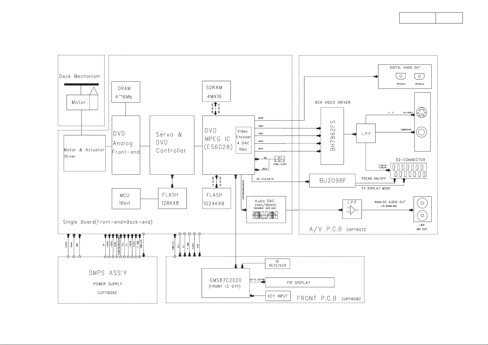
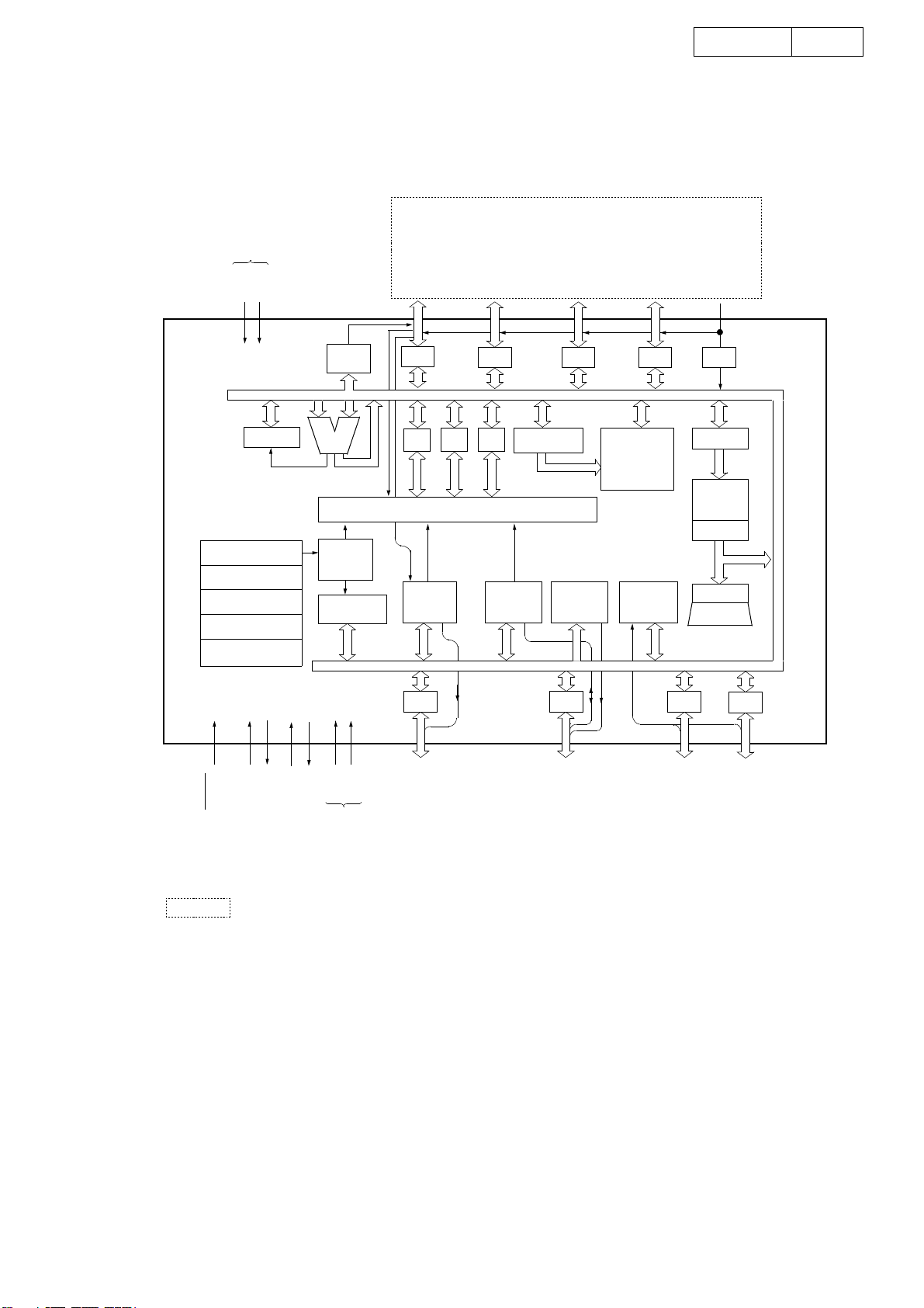
BLOCK DIAGRAM
DVD-310
3
3
半導体一覧表
Only major semiconductors are shown, general semiconductors etc. are omitted to list.
主な半導体を記載しています。汎用の半導体は記載を省略しています。
●
IC's
Note: Abbreviation ahead of IC No. indicates the name of P.W.B., etc.
注 ): IC No. の前の記号は、基板の名称を表します。
AV: A/V P.W.B. ME: MECHA P.W.B.
FR: FRONT P.W.B. SM: SMPS P.W.B.
ES6028FW (ME: U9)
VSS
HA1
HA0
HCS3FX#
HCS1FX#
HIOCS16#
HRD#
HWR#
VEE
VSS
HIORDY
HRST#
HIRQ
HRDQ#
HWRQ#
HD15
HD14
VCC
VSS
HD13
HD12
HD11
HD10
HD9
HD8
HD7
VEE
VSS
HD6
HD5
HD4
HD3
HD2
HD1
HD0
VCC
156
155
154
153
152
151
150
149
148
147
146
145
144
143
142
141
140
139
138
137
136
135
134
133
132
131
130
129
128
127
126
125
124
123
122
VEE
157
HA2
158
VEE
159
AUX[0]
160
AUX[1]
161
AUX[2]
162
VSS
163
VEE
164
AUX[3]
165
AUX[4]
166
AUX[5]
167
AUX[6]
168
AUX[7]
169
LOE#
170
VSS
171
VCC
172
LCS0#
173
LCS1#
174
LCS2#
175
LCS3#
176
VSS
177
LD0
178
LD1
179
LD2
180
LD3
181
LD4
182
VEE
183
VSS
184
LD5
185
LD6
186
LD7
187
LD8
188
LD9
189
LD10
190
LD11
191
VSS
192
VEE
193
LD12
194
LD13
195
LD14
196
LD15
197
LWRLL#
198
LWRHL#
199
VSS
200
VEE
201
CAMIN0
202
CAMIN1
203
LA0
204
LA1
205
LA2
206
LA3
207
VSS
208
123456789101112131415161718192021222324252627282930313233343536373839404142434445464748495051
LA4
LA5
LA6
LA7
LA8
VEE
LA9
VSS
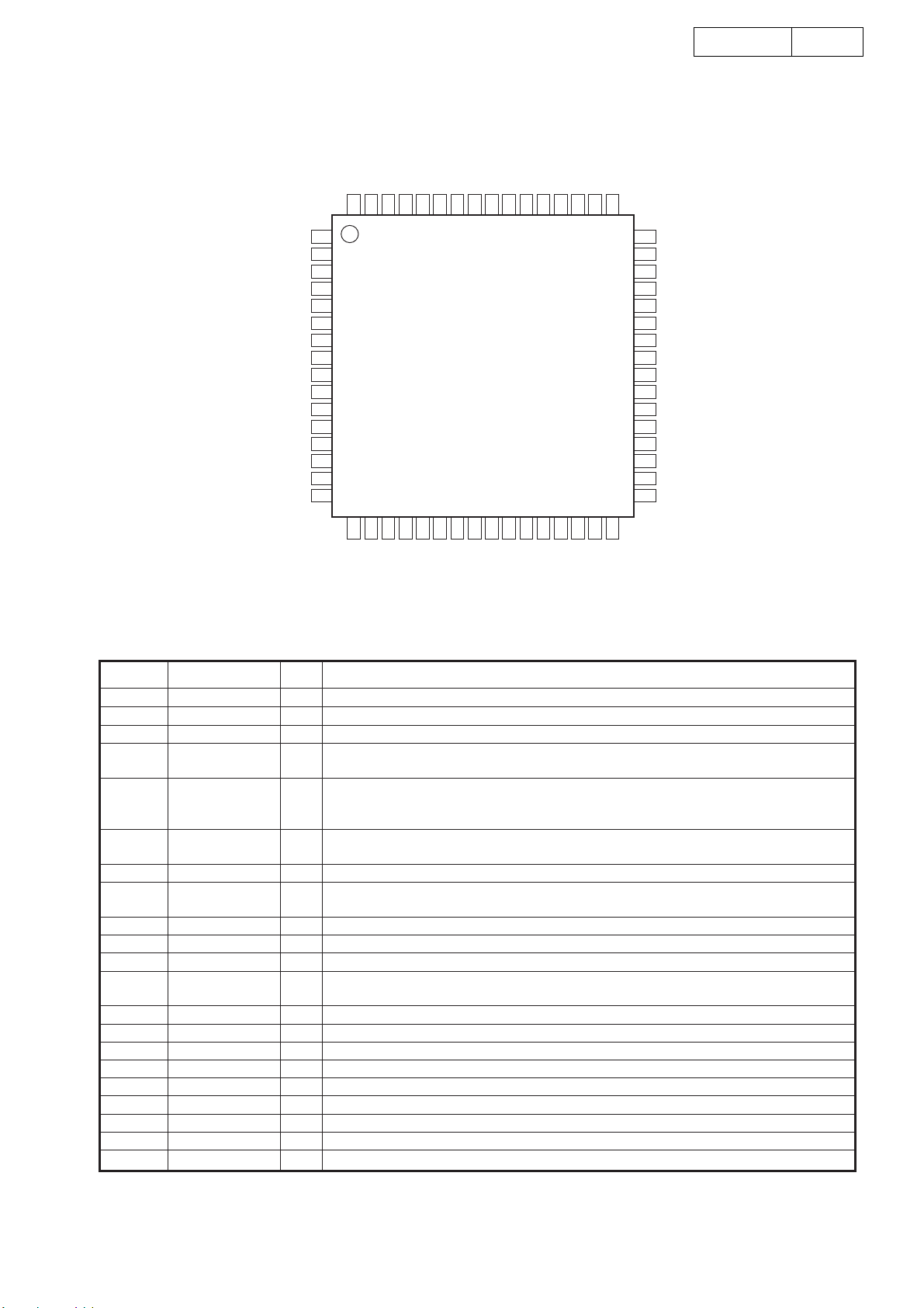
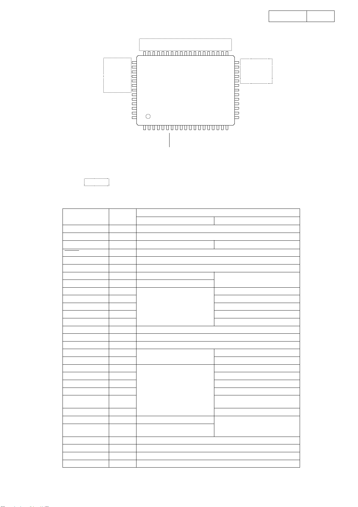
ES6038 Terminal Function
VCC
VSS
VSS
LA10
LA11
LA12
LA13
VEE
LA14
LA15
LA16
LA17
LA18
LA19
LA20
VEE
LA21
TDMDX
RESET#
TDMFS
TDMDR
TDMCLK
TDMTSC#
121
VSS
VCC
TWS/SEL_PLL2
TSD0/SEL_PLL0
TSD1/SEL_PLL1
VSS
120
TSD2
HSYNC#
VSYNC#
119
118
TSD3
MCLK
PCLKQSCN
PCLK2XSCN
YUV7
117
116
115
NC
TBCK
SPDIF/PLL3
YUV6
114
VSS
YUV5
113
VCC
VSS
112
RSD
ADVEE
111
RWS
YUV4
110
RBCK
YUV3
109
NC
DVD-310
YUV2
YUV1
YUV0
DCLK
108
107
106
105
52
XIN
VSS
AVEE
XOUT
4
104
VEE
103
VSS
102
DSCK
101
DQM
100
DCS0#
99
VEE
98
VSS
97
DCS1#
96
DB15
95
DB14
94
DB13
93
DB12
92
VEE
91
VSS
90
DB11
89
DB10
88
DB9
87
DB8
86
DB7
85
DB6
84
VSS
83
VCC
82
DB5
81
DB4
80
DB3
79
DB2
78
DB1
77
DB0
76
VSS
75
VEE
74
DMBS1
73
DMBS0
72
DRAS#
71
DWE#
70
DSCK_EN
69
DCAS#
68
VEE
67
VSS
66
DMA11
65
DMA10
64
DMA9
63
DMA8
62
DMA7
61
DMA6
60
VSS
59
VEE
58
DMA5
57
DMA4
56
DMA3
55
DMA2
54
DMA1
53
DMA0
1, 18, 27, 59,
68, 75, 92, 99,
104, 130, 148, VEE I I/O power supply.
157, 159, 164,
183, 193, 201
8, 17, 26, 34,
43, 52, 60, 67,
76, 84, 91, 98,
103, 112, 120, VSS I Ground.
129, 138, 147,
156, 163, 171,
177, 184, 192,
200, 208
23:19, 16:10,
7:2, 207:204
9, 35, 44, 83,
121, 139, 172
LA[21:0] O Device address output.
VCC I Core power supply.
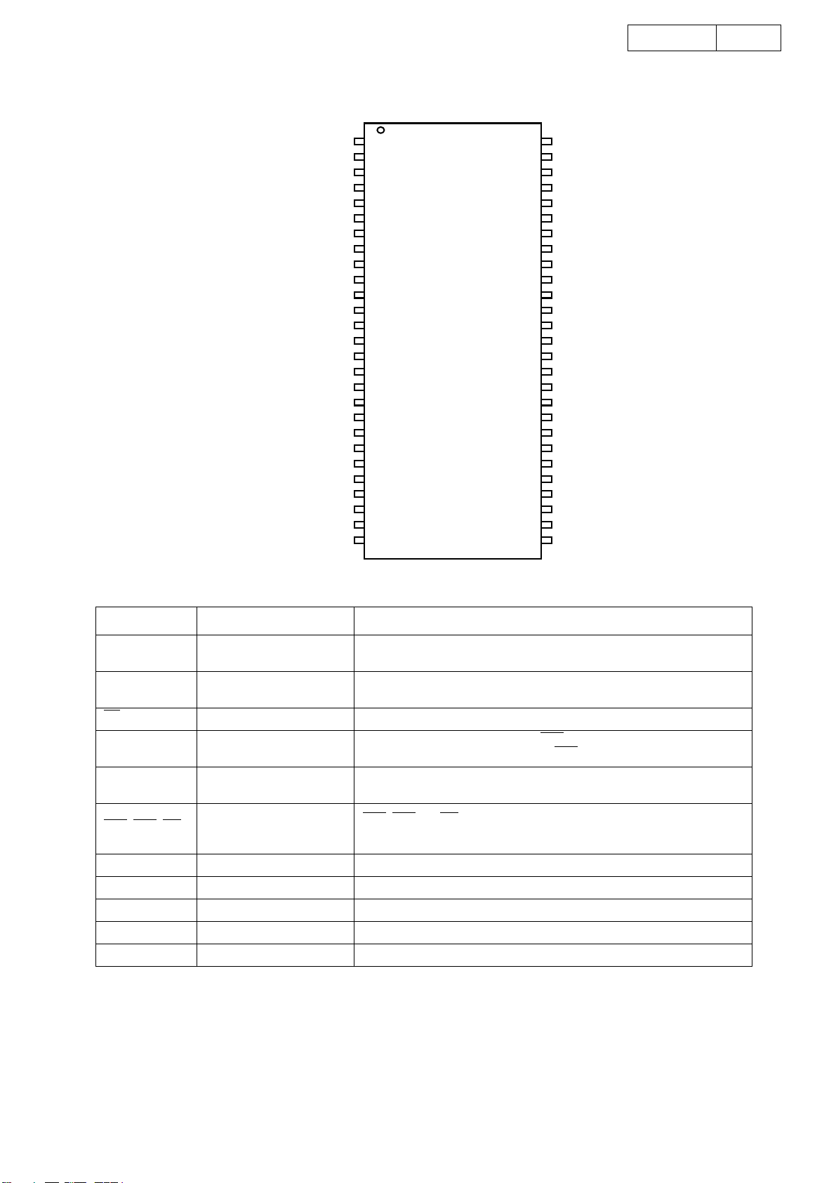
FunctionI/OPin No. Pin Name
4
DVD-310
5
Pin No. Pin Name
24 RESET# I Reset input, active low.
25 TDMDX O TDM transmit data.
28 TDMDR I TDM receive data.
29 TDMCLK I TDM clock input.
30 TDMFS I TDM frame sync.
31 TDMTSC# O TDM output enable.
TWS O Audio transmit frame sync.
SEL_PLL2 I System and DSCK output clock frequency selection is made at the rising edge of RESET#.
The matrix below lists the available clock frequencies and their respective PLL bit settings.
SEL_PLL2 SEL_PLL1 SEL_PLL0 Clock Type
0 0 0 VCO off.
0 0 1 DCLK
32 0 1 0 Bypass mode
0 1 1 DCLK x 2
1 0 0 DCLK x 4.5
1 0 1 DCLK x 3
1 1 0 DCLK x 3.5z
1 1 1 DCLK x 4
33
36
37 TSD[2] O Audio transmit serial data output 2.
38 TSD[3] O Audio transmit serial data output 3.
39 MCLK I/O Audio master clock for audio DAC.
40 TBCK O Audio transmit bit clock.
41 SEL_PLL3 Clock Source
42,48 NC No connect pins. Leave open.
45 RSD I Audio receive serial data.
46 RWS I Audio receive frame sync.
47 RBCK I Audio receive bit clock.
49 XIN I Crystal input.
50 XOUT O Crystal output.
51 AVEE I Analog power for PLL.
66:61, 58:53 DMA[11:0] O DRAM address bus [11:0]
69 DCAS# O DRAM column address strobe,
70 DSCK_EN O DRAM clock enable.
71 DWE# O DRAM write enable.
72 DRAS# O DRAM row address strobe.
73 DMBS0 O SDRAM bank select 0.
74 DMBS1 O SDRAM bank select 1.
96:93, 90:85,
82:77
97, 100 DCS[1:0]# O SDRAM chip select [1:0]
101 DQM O Data input/output mask.
102 DSCK O Output clock to SDRAM.
105 DCLK I 27 MHz clock input to PLL.
106 UDAC O Video UDAC output.
107 VREF I Internal voltage to video DAC.
108 CDAC O Video CDAC output.
109 COMP I Compensation input.
110 RSET I DAC current adjustment resistor input.
111 ADVEE I Analog power for video DAC.
113 YDAC O Video YDAC output.
TSD0 O Audio transmit serial data port 0.
SEL_PLL0 I Refer to the description and matrix for SEL_PLL2 pin 32.
TSD1 O Audio transmit serial data port 1.
SEL_PLL1 I Refer to the description and matrix for SEL_PLL2 pin 32.
SPDIF O S/PDIF output.
SEL_PLL3 I Clock source select.
0 Crystal oscillator
1 DCLK input
DB[15:0] I/O DRAM data bus [15:0]
FunctionI/O
5
DVD-310
6
Pin No. Pin Name
114 VDAC O Video VDAC output.
115 YUV7 O YUV7 pixel output data.
116 PCLK2XSCN I/O 27 MHz video output pixel clock.
117 PCLKQSCN O 13.5 MHz video output pixel clock.
118 VSYNC# I/O Vertical sync, active low.
119 HSYNC# I/O Horizontal sync, active low.
127:122 HD[5:0] I/O Host data I/O [5:0].
128 HD[6] I/O Host data I/O [6].
131 HD[7] I/O Host data I/O [7].
132 HD[8] I/O Host data bus 8.
133 HD[9] I/O Host data bus line 9.
134 HD[10] I/O Host data bus line 10.
135 HD[11] I/O Host data bus line 11.
136 HD[12] I/O Host data bus line 12.
137 HD[13] I/O Host data bus line 13.
140 HD[14] I/O Host data bus line 14.
141 HD[15] I/O Host data bus line 15.
142 HWRQ# O Host write request.
143 HRRQ# O Host read request.
144 HIRQ I/O Host interrupt.
145 HRST# O Host reset.
146 HIORDY I Host I/O ready.
149 HWR# I/O Host write.
150 HRD# O Host read.
151 HIOCS16# I Device16-bit data transfer.
152 HCS1FX# O Host select 1.
153 HCS3FX# O Host select 3.
158, 155:154 HA[2:0] I/O Host address bus.
160 AUX[0] O I2C DATA.
162 AUX[2] I/O Auxiliary ports 2.
165 AUX[3] I/O Auxiliary ports 3.
169:166 AUX[7:3] I/O Auxiliary ports 7:3.
170 LOE# O Device output enable.
176:173 LCS[3:0]# O Chip select [3:0].
197:194,
191:185, LD[15:0] I/O EPROM device data bus.
182:178
198 LWRLL# O Device low-byte write enable.
199 LWRHL# O Device high-byte write enable.
202 CAMIN0 I Camera YUV 0.
203 CAMIN1 I Camera YUV 1.
161 AUX[1]OI2C CLK.
FunctionI/O
6
M5705 (ME: U1)
AVSS-DS
XSRFIN
XSIPIN
AVDD5-DS
XSDSSLV
XSRSLINT
XSAWRC
XSRFGC
XSEFGC
XSFOCUS
XSTRACK
XSSLEG
AVDD5-DA
XSMOTOR
AVSS-DA
XSRFRPLP
XSTELP
XSVREF2
XSRFRP
XSTEXI
AVSS-AD
XSTEI
XSFEI
XSAEI
AVDD5-AD
XSSBAD
XSDFCT
XSCSJ
XSCLK
XSDATA
XSLDC
XSFGIN
XSSPDON
XSFLAG(3)
XSFLAG(2)
XSFLAG(1)
XSFLAG(0)
XMP1_7
XMP1_6
XMP1_4
XSAWRCVCO
XSVREFO
XSPDOFTR2
XSVR_PLL
XSFTROPI
XSFDO
AVSS_PL
XSPLLFTR2
AVDD5_PL
XSFDIREF
XSPDIREF
GND
XTSLRF
XTPLCK
VDD
XRA(3)
XRA(2)
XRA(1)
XRA(0)
XRA(4)
XRA(5)
XRA(6)
GND
XRA(7)
XRA(10)
XRA(11)
VDD
XRA(8)
XRA(9)
XROEJ
VDD
176
175
174
173
172
171
170
169
168
167
166
165
164
163
162
161
160
159
158
157
156
155
154
153
152
151
150
149
148
147
XMD(7)
146
XMCSJ
XMRDJ
XMWRJ
XMA(11)
XMA(10)
XMINT1J
1
2
3
4
5
6
VDD
7
8
9
10
11
12
13
14
15
16
17
18
19
20
21
22
23
24
25
26
27
GND
28
29
30
31
32
33
34
35
36
37
38
39
40
41
GND
42
NC
43
44
45464748495051525354555657585960616263646566676869707172737475767778798081828384858687
VDD
VDD
GND
XOSC1
XOSC2
XMALE
XMD(0)
XMD(1)
XMD(2)
XMD(3)
XMD(4)
XMD(5)
XMP1_3
XMFSCSJ
XMP1_2
XMP1_1
XGPIO(2)
M5705
XMRSTJ
XGPO(1)
XCRSTJ
XGPO(0)
XMPSENJ
XMP1_0
XMD(6)
4M DRAM
XRCASJ
XRRASJ
145
144
VDD
XMA(9)
XRSDCLK
XRWEJ
143
142
XMA(8)
XMA(7)
XRD(7)
141
XMA(6)
XRD(8)
140
XMA(5)
XRD(6)
139
XMA(4)
GND
138
XMA(3)
XRD(9)
137
XMA(2)
XRD(5)
136
XMA(1)
XRD(10)
XRD(4)
135
134
XMA(0)
XMA(12)
XRD(11)
133
132
131
130
129
128
127
126
125
124
123
122
121
120
119
118
117
116
115
114
113
112
111
110
109
108
107
106
105
104
103
102
101
100
88
GND
99
98
97
96
95
94
93
92
91
90
89
XRD(3)
XRD(12)
GND
XRD(2)
XRD(13)
XRD(1)
XRD(14)
XRD(0)
XRD(15)
XHD(7)
XHD(8)
XHD(6)
XHD(9)
XHD(5)
XHD(10)
XHD(4)
XHD(11)
VDD
XHD(3)
XHD(12)
XHD(2)
XHD(13)
GND
XHD(1)
XHD(14)
XHD(0)
XHD(15)
XHDRQ
XHIOWJ
XHIORJ
XHIORDY
XHDACKJ
XHINT
XHCS16J
XHA(1)
XHPDIAGJ
XHA(0)
XHA(2)
XHCS1J
XHCS3J
XHDASPJ
XMA(15)
XMA(14)
XMA(13)
DVD-310
7
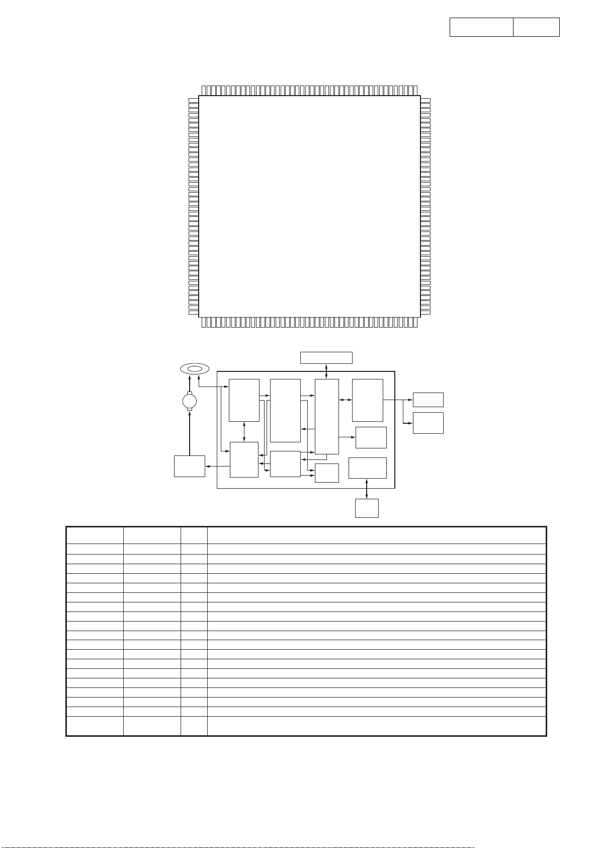
ATAPI
M
Motor
Driver
Data
Separator
Digital
Servo
DVD-DSP
CD-DSP
RAM
Arbiter
Target
Search
&
MPEG
I/F
C3 ECC
EDC
MCU
ROM
M5705 Terminal Function
Pin Name
Type
2 XSRFIN I/A Analog RF signal input after passing through the equalizer
3 XSIPIN I/A Inverting input pin of data slicer
5 XSDSSLV O/A Slice level output pin
6 XSRSLINT I/A Reference current setting pin for analog data slicer
8 XSAWRC O/A Output for enlarge VCO range. Analog output from DAC buffer
9 XSRFGC O/A RF gain control output
10 XSEFGC O/A E,F gain control output
11 XSFOCUS O/A Output voltage level for focusing buffer IC
12 XSTRACK O/A Output voltage level for tracking buffer IC
13 XSSLEG O/A Output voltage level for sledge buffer IC
15 XSMOTOR O/A Output voltage level for spindle motor buffer IC
17 XSRFRPLP I/A High bandwidth low pass filter input for RFRP
18 XSTELP I/A High bandwidth low pass filter input for TE
19 XSVREF2 I/A 2.1V reference voltage input
20 XSRFRP I/A RF ripple/envelope signal input
21 XSTEXI I/A Tracking zero crossing input signal
23 XSTEI I/A Tracking error input signal
24 XSFEI I/A Focus error input signal
25 XSCEI I/A
1. Center error input signal
2. Photo Interrupt input
DescriptionPin No.
PC
MPEG
DEC.
7
DVD-310
8
Pin Name
27 XSSBAD I/A Sub-beam addition signal input
166 XSPDIREF I/A
167 XSFDIREF I/A
169 XSPLLFTR2 I/A Data PLL loop filter pin#2
171 XSFDO O/A Output node of frequency detector charge pump circuit
172 XSFTROPI I/A Input node of loop filter OP circuit
173 XSVR_PLL I/A PLL reference voltage input
174 XSPDOFTR2 I/A Phase detector filter pin#1
175 XSVREFO O/A Reference voltage output
176 XSAWRCVCO I/A Auto Wide Range Control of VCO input pin. For enlarge VCO range in CAV mode
29 XSDFCT I Detect detection signal input
30 XSCSJ O Chip select signal for accessing control registers
31 XSCLK O Clock output for accessing control registers
32 XSDATA I/O Registers data input/output pin
33 XSLDC O Laser diode on/off control output for both CD/DVD
34 XSFGIN I Motor Hall sensor input
35 XSSPDON O Spindle motor on output
36, 37, 38, 39 XSFLAG[3:0] O These pins are used to monitor some status of ser vo control block
48, 51, 52 XGPIO[2:0] I/O
40 XMP1_7 I/O Internal microcontroller programmable I/O port 1.7.
41 XMP1_6 I/O Internal microcontroller programmable I/O port 1.6.
43 XMP1_5 I/O This pin is now changed to be NC.
44 XMP1_4 I/O Internal microcontroller programmable I/O port 1.4.
45 XMP1_3 I/O Internal microcontroller programmable I/O port 1.3.
47 XMP1_2 I/O Internal microcontroller programmable I/O port 1.2.
49 XMP1_1 I/O Internal microcontroller programmable I/O port 1.1.
57 XMP1_0 I/O
46 XMFSCSJ I/O Output chip select connected to external flash ROM chip enable pin
54 XMPSENJ I/O Output program store enable connected to external ROM PSENJ pin.
56 XMALE I/O This signal is used as address latch signal in address/data mux mode
70 XMCSJ I/O
71 XMRDJ I/O
72 XMWRJ I/O This signal is used as the Wire Strobe signal
73 XMINT1J I/O
74, 75, 77, 78,
79, 80, 81, 82,
83, 84, 85, 86,
87, 89, 90, 91
62, 63, 64, 65,
66, 67, 68, 69 bus for the 8-bit processor mode.
163 XTPLCK I/O PLCK test pin
164 XTSLRF I/O SLRF test pin
59 XOSC1 I Crystal input/System clock. The input frequency from outside crystal or oscillator is 33.8688MHz
60 XOSC2 O Crystal output
53 XCRSTJ I
94 XHCS1J I This pin is used to select the command block task file registers
93 XHCS3J I This pin is used to select the control block task file registers
103 XHIORJ I Asserted by the host during a host I/O read operation
104 XHIOWJ I Asserted by the host during a host I/O write operation
105 XHDRQ O
101 XHDACKJ I
99 XHCS16J O
50 XHRSTJ I Host Reset. The reset of ATA bus
100 XHINT O
XMA[15:0] I/O These pins are used as address bus
XMD[7:0] I/O
Type
Phase detector reference current generator. Connect a resistor between this pin and
ground to set reference current
Frequency detector reference current generator. Connect a resistor between this pin and
ground to set reference current
1. These pins are used as general purpose I/O bus
2. When use internal microcontroller, XGPIO[2] can be used as programmable I/O port 3.6.
Internal microcontroller programmable I/O port 1.0.
This pin is default used as the A16 (microcontroller address line 16)
1. This signal must be asserted for all microcontroller accesses to the register of this chip
2. When use internal microcontroller, this signal can be used as programmable I/O port 3.1
1. This signal is used as the Read Strobe signal
2. When use internal microcontroller, this signal can be used as programmable I/O port 3.0
1. This signal is an interrupt line to the microcontroller
2. When use internal microcontroller, this signal can be used as programmable I/O port 3.7
These pins are used as data bus for the 16-bit processor mode, or the address/data mux
Chip Reset. As asserted low input generates a component reset that stops all operations within
the chip and deasserts all output signals. All input/output signals are set to input.
DMA request. This pin is configured as the DMA request signal, and is used during DMA transfer
1.
between the host and the controller. This pin is tri-stated when DMA transfers are not enabled.
2.
MPEG acknowledge. This pin is used as the ACKJ signal when MPEG interface mode is selected.
1. DMA acknowledge. This pin is configured as DACKJ, and is used as the DMA acknowledge
signal during DMA data transfers.
2. MPEG request. This pin is used as the REQ signal when MPEG interface mode is selected
1. 16-bit data select. This signal indicates that a 16-bit data transfer is active on the host data
bus. This pin is open-drain tri-state output.
2. MPEG clock. This pin is used as the CLOCK signal when MPEG interface mode is selected.
1. Host interface request. This tri-state pin is the host interrupt request, and is asserted to
indicate to the host that the controller needs attention.
2. MPEG begin. This pin is used as the BEGIN signal when MPEG interface mode is selected
DescriptionPin No.
8
DVD-310
9
Pin Name
97 XHPDIAGJ I/O This pin is used as the Passed Diagnostics signal, and may be an input or an open-drain output
92 XHDASPJ I/O
102 XHIORDY I/O
95, 96, 98 XHA[2:0] I
106, 107, 108, 2.
109, 111, 112, 3. VCD I/F. Bit3-0 are used as VCD I/F signal when VCD function is enabled. The relationship of
113, 114, 116, bit3-0 and VCD I/F is as follow
117, 118, 119, HD0—CD-DATA
120, 121, 122, HD1—CD-LRCK
123 HD2—CD-BCK
143 XRSDCLK O This signal is the clock output for SDRAM
147 XROEJ O
142 XRWEJ O This signal is asserted low when a buffer memory write operation is active
144 XRRASJ O
145 XRCASJ O
148, 149, 151,
152, 153, 155,
156, 157, 158,
159, 160, 161
124, 125, 126,
127, 128, 129,
131, 132, 134,
135, 136, 137,
138, 139, 140,
141
4 AVDD5_DS Analog Power +5V for Data Slicer part
14 AVDD5_DA Analog Power +5V for DAC part
26 AVDD5_AD Analog Power +5V for ADC part
168 AVDD5_PL Analog Power +5V for Data PLL part
7, 55, 58, 76,
115, 146,
150, 162
1 AVSS_DS Analog Ground for Data Slicer part
16 AVSS_DA Analog Ground for DAC part
22 AVSS_AD Analog Ground for ADC part
170 AVSS_PL Analog Ground for Data PLL part
28, 42, 61,
88, 110, 130,
138, 154, 165
XHD[15.0] I/O
XRA[11:0] O 1: Normal operation
XRD[15:0] I/O These signals are the 8-bit parallel data lines to/from the buffer memory.
VDD Power +3.3V for digital core logic and pad
GND Digital Ground core logic and pad.
Type
This pin is used as the Drive Active/Slave Present signal, and is an input or an open-drain
output. This pin is used for Master/Slave drive communication and/or for driving an LED
1. I/O channel ready. This signal is driven low to extend host transfer cycles when the controller
is not ready to respond. This pin will be tri-stated when a read or write is not in progress.
2. MPEG error. This pin is used as the ERROR signal when MPEG interface mode is selected
Host address lines. The host address lines A[2:0] are used to access the various host control,
status, and data registers
1. Host data bus. This bus is used to transfer data and status between the host and the controller.
MPEG data bus 7-8. The HD[7:0] are used as the DATA [7:0] when MPEG interface mode is selected.
HD3—CD-C2PO
This signal is used as the memory output enable for external DRAM buffers. After RSTJ is
asserted, this signal will be low
This signal is used as Row address output to external DRAM buffer. After RSTJ is asserted, this
signal will be high
This signal is used as column address output to external DRAM. After RSTJ is asserted, this
signal will be high
1. RAM address lines. These are bits11-0 for addressing the buffer memory.
2. Hardware setting. The bits6-0 are used as hardware setting for some functions.
RA[9] : FLASH size is 64K/128K
1: FLASH size is 64K
0: FLASH size is 128K
RA[8] : External CPU is 8032/H8
1: 8032
0: H8
RA[7] : Microcontroller programmable I/O port 1 pin control
1: By internal microcontroller
0: By registers to decide input/output
RA[6] : System test pin output
0: System test pin output
RA[5] : For testing purpose, don’t need to set
RA[4] : IDE master/slave
1: Slave
0: Master
RA[3] : For testing purpose, don’t need to set
RA[2] : For testing purpose, don’t need to set
RA[1-0] : MCU Mode selection
11: Normal Mode (internal uP, internal address latch)
10: Outside uP Mode (ICE Mode)
01: Test mode for internal uP testing
00: Internal uP mode with external address latch
DescriptionPin No.
9
SP3721A (ME: U2)
CDRF
CDRDDC
ATOP
ATON
AIN
AIP
DVD-310
HOLD1
VNA
FNN
FNP
DIP
DIN
RX
BYP
SIGO
VPA
49505152535455565758596061626364
10
DVDRFP
DVDRFN
PD1
PD2
A2
B2
C2
D2
CP
CN
1
2
3
4
5
6
7
8
9
10
11
D
12
C
13
B
14
A
15
F
16
E
NC
VCI2
CDTE
TOP VIEW
VNB
DVDLD
DVDPD
CDPD
CDLD
LDON#
VC
VCI
VPB
VIIRR
VIP
32313029282726252423222120191817
VIB
48
47
46
45
44
43
42
41
40
39
38
37
36
35
34
33
FDCHG#
SDEN
SD ATA
SCLK
LCP
LCN
CE
FE
TE
MEI
MEV
TPH
DFT
PI
MIN
MEVO
MLPF
SP3721A Terminal Function
Pin Name
Type
1, 2 DVDREP, DVDREN I RF Signal Inputs. Differential RF signal attenuator input pins
63 CDRF I RF Signal Inputs. Single-ended RF signal attenuator input pin
59, 60 AIP, AIN I AGC Amplifier Inputs. Differential AGC amplifier input pins
53, 54 DIP, DIN I
Analog inputs for RF Single Buffer. Differential analog inputs to the RF single-ended output buffer
and full wave rectifier
Low Impedance Enable. A TTL compatible input pin that activates the FDCHG switches. A low
32 FDCHG# I
level activates the switches and the falling edge of the internal FDCHG triggers the fast decay for
the MIRR bottom hold circuit. (open high)
49 HOLD1 I
Hold Control. A TLL compatible control pin which, when pulled high, disables the RF AGC charge
pump and holds the RF AGC amplifier gain at its present value. (open high)
11~14 D, C, B, A I Photo Detector Interface Inputs. Inputs from the main beam Photo detector matrix outputs
5~8 A2, B2, C2, D2 I
Photo Detector Interface Inputs. AC coupled inputs for the DPD from the main beam Photo
detector matrix outputs
15~16 F, E I CD tracking Error Inputs. Inputs from the CD photo detector error outputs.
3~4 PD1, PD2 I CD Photo detector Interface Inputs. Inputs from the CD photo detector error outputs
40 MEI I Mirror Envelope Inputs. The SIGO envelope input pin
35 MIN I
RF signal Input for Mirror. AC coupled inputs for the mirror detection circuit from the pull-in signal
output. (PI)
21 DVDPD I APC Input. DVD APC input pin from the monitor photo diode
23 CDPD I APC Input. CD APC input pin from the monitor photo diode
25 LDON# I APC Output On/Off. APC output control pin. A low level activates the LD output. (open high)
61, 62 ATON/ATOP O Differential Attenuator Output. Attenuator outputs
51, 52 FNN, FNP O Differential Normal Output. Filter normal outputs
57 SIGO O Single Ended Normal Output. Single-ended RF output
64 CDRFDC O CD RF Signal Output. Single ended CD RF summing output
42 FE O Focusing Error Signal Output. Focus error output reference to VCI
41 TE O Tracking Error Signal Output. Tracking error output reference to VCI
DescriptionPin No.
10
DVD-310
11
Pin Name
43 CE O Center Error Signal Output. Center error output reference to VCI
34 NEVO O SIGO Bottom Envelope Output. Bottom envelope for mirror detection
37 DFT O
29 MIRR O Mirror Detect Output. Mirror Detect comparator output. Pseudo CMOS output
36 PI O
22 DVDLD O APC output. DVD APC output pin to control the laser power
24 CDLD O APC output. CD APC output pin to control the laser power
56 BYP I/O The RF AGC integration capacitor CBYP, is connected between BYP and VPA
9 CP I/O
10 CN I/O
45 LCP — Center Error LPF pin. An external capacitance is connected between this pin and the LCN pin
44 LCN — Center Error LPF pin. An external capacitance is connected between this pin and the LCP pin
30 MP — MIRR signal Peak hold pin. An external capacitance is connected to between this pin and VPB
31 MB — MIRR signal Bottom hold pin. An external capacitance is connected to between this pin and VPB
39 MEV — Sigo Bottom Envelope pin. An external capacitance is connected to between this pin and VPB
17 CDTE — CD Tracking. E-F Opamp output for feedback
38 TPH — PI Top Hold pin. An external capacitance is connected to between this pin and VPB
26 VC —
27 VCI — Reference Voltage input. DC bias voltage input for the servo input reference
18 VCI2 — Reference Voltage input. DC bias voltage input for the servo input reference
55 RX —
33 MLPF — MIRR signal LPF pin. An external capacitance is connected between this pin and VPB
19 NC — No Connect
48 SDEN I
47 SDATA I/O
46 SCLK I
58 VPA Power. Power supply pin for the RF block and serial port
28 VPB Power. Power supply pin for the servo block
50 VNA Ground. Ground pin for the RF block and serial port
20 VNB Ground. Ground pin for the servo bolck
Type
Defect Output. Pseudo CMOS output. When a defect is detected, the DFT output goes high. Also
the servo AGC output can be monitored at this pin, when CAR bits 7-4 are ‘0011’
Pull-in Signal Output. The summing signal output of A, B, C, D or PD1, PD2 for mirror detection.
Reference to VCI
Differential Phase tracking LPF pin. An external capacitance is connected between this pin and
the CN pin
Differential Phase tracking LPF pin. An external capacitance is connected between this pin and
the CP pin
Reference Voltage output. This pin provides the internal DC bias reference voltage (+2.5V lix).
Output Impedance is less than 50ohms
Reference Resistor Input. An external 8.2kohm, 1% resistor is connected from this pin to ground
to establish a precise PTAT (proportional to absolute temperature) reference current for the filter
Serial Data Enable. Serial Enable CMOS input. A high level input enable the serial port (Not to be
left open)
Serial Data. Serial data bi-directional CMOS pin. NRZ programming data for the internal registers
is applied to this input ( Not to be left open)
Serial Clock. Serial Clock CMOS input. The clock applied to this pin is synchronized with the data
applied to SDATA (Not to be left open)
DescriptionPin No.
11
GMS87C2020Q (FR: IC91)
BLOCK DIAGRAM
ADC Power
Supply
SS
AVDDAV
R07
R06
R05
R04
R03/BUZO
R02/EC0
R01/INT1
R00/INT0
R10~R17
R20~R27
R30~R35
DVD-310
Vdisp/RA
12
PSW
Syst
em controller
System
Clock Controller
Sub System
Clock Controller
Timing generator
Cloc k
Genera tor
IN
X
OUT
RESET
X
SX
IN
SX
Driver
Buzzer
ALU
8-bit Basic
Interval
Timer
Watchdog
Timer
DD
OUT
V
Power
Supply
R0
A
Interrupt Controller
8-bit
Timer/
Counter
R4 R5
R40 / T0O
R41
SS
V
R42
R43 R73 / AN11
X Y
R1
Stack Pointer
8-bit serial
Interface
R2
Data Memory
(448 bytes)
10-bit
PWM
R50
R51
R52
R53 / SCLK
R54 / SIN
R55 / SOUT
R56 / PWM1O/T1O
R57
8-bit
ADC
R3
R60 / AN0
R61 / AN1
R62 / AN2
R63 / AN3
R64 / AN4
R65 / AN5
R66 / AN6
R67 / AN7
Program
Memory
Data Table
R6
RA
PC
PC
R7
R70 / AN8
R71 / AN9
R72 / AN10
High Voltage Port
12
64MQFP
R30
R31
R32
R33
R34
R35
V
RA
disp
T0O
R40
R41
R42
R43
R50
R51
High Voltage Port
R27
R25
R24
R23
R26
515049
52
53
54
55
56
57
58
59
60
61
62
63
64
484746
123456789
R53
R52
R54
R55
R56
SIN
SCLK
SOUT
PWM1O/T1O
R22
R21
R20
R17
R16
R15
45
4443424140
GMS81C2012/20
101112131415161718
XI
SS
XO
V
R57
RESET
R74
SXI
R14
R13
R12
39
3837363534
SS
R75
R60
AV
AN0
SXO
DVD-310
R11
R10
R07
R06
R05
33
R04
32
R03
R02
R01
R00
DD
V
AV
R73
R72
R71
R70
R67
R66
DD
BUZO
EC0
INT1
INT0
AN11
AN10
AN9
AN8
AN7
AN6
31
30
29
28
27
26
25
24
23
22
21
20
19
R61
R62
R63
R64
R65
AN1
AN2
AN3
AN4
AN5
13
PIN NAME In/Out
DD
V
SS
V
)
RA (V
disp
RESET
Basic Alternate
- Supply voltage
- Circuit ground
I(I) 1-bit high-voltage Input only port High-voltage input power supply pin
I Reset signal input
Function
XIN I Oscillation input
XOUT O Oscillation output
SXIN(R74) I Sub Oscillation input
SXOUT(R75) O Sub Oscillation output
R00 (INT0) I/O (I)
General I/O ports
External interrupt 0 input
R01 (INT1) I/O (I) External interrupt 1 input
R02 (EC0) I/O (I) Timer/Counter 0 external input
8-bit high-voltage I/O ports
R03 (BUZO) I/O (O) Buzzer driving output
R04~R07 I/O
R10~R17 I/O 8-bit high-voltage I/O ports
R20~R27 I/O 8-bit high-voltage I/O ports
R30~R35 I/O 6-bit high-voltage I/O ports
R40 (T0O) I/O (O)
R41~R43 I/O
4-bit general I/O ports
Timer/Counter 0 output
R50~R52 I/O
R53 (SCLK) I/O (I/O) Serial clock source
R54 (SIN) I/O (I) Serial data input
R55 (SOUT) I/O (O) Serial data output
R56 (PWM1O/T1O) I/O (O)
8-bit general I/O ports
PWM 1 pulse output /Timer/Counter 1 output
R57 I/O
R60~R67 (AN0~AN7) I/O (I) 8-bit general I/O ports
R70~R73
(AN8~AN11)
DD
AV
SS
AV
DD
V
SS
V
I/O (I) 4-bit general I/O ports
- Supply voltage input pin for ADC
- Ground level input pin for ADC
- Supply voltage
- Circuit ground
Analog voltage input
Port Function Description
13
HY57V65120BTC-75 (ME: U11)
DVD-310
14
DD
V
DQ0
V
DDQ
DQ1
DQ2
SSQ
V
DQ3
DQ4
DDQ
V
DQ5
DQ6
V
SSQ
DQ7
DD
V
LDQM
/WE
/CAS
/RAS
/CS
BA0
BA1
A10/ AP
A0
A1
A2
A3
V
DD
1
2
3
4
5
6
7
8
9
10
11
12
13
14
15
16
17
18
19
20
21
22
23
24
25
26
27
54
53
52
51
50
49
48
47
46
45
44
43
42
41
40
39
38
37
36
35
34
33
32
31
30
29
28
SS
V
DQ15
V
SSQ
DQ14
DQ13
DDQ
V
DQ12
DQ11
SSQ
V
DQ10
DQ9
V
DDQ
DQ8
SS
V
NC
UDQM
CLK
CKE
NC
A11
A9
A8
A7
A6
A5
A4
V
SS
PIN DESCRIPTION
PIN PIN NAME DESCRIPTION
CLK Clock
CKE Clock Enable
CS
BA0,BA1 Bank Address
A0 ~ A11 Address
RAS
, CAS, WE
LDQM, UDQM Data Input/Output Mask Controls output buffers in read mode and masks input data in write mode
DQ0 ~ DQ15 Data Input/Output Multiplexed data input / output pin
V
DD/VSS Power Supply/Ground Power supply for internal circuits and input buffers
V
DDQ/VSSQ Data Output Power/Ground Power supply for output buffers
NC No Connection No connection
Chip Select Enables or disables all inputs except CLK, CKE and DQM
Row Address Strobe,
Column Address Strobe,
Write Enable
The system clock input. All other inputs are registered to the SDRAM on the
rising edge of CLK
Controls internal clock signal and when deactivated, the SDRAM will be one
of the states among power down, suspend or self refresh
Selects bank to be activated during RAS activity
Selects bank to be read/written during CAS
Row Address : RA0 ~ RA11, Column Address : CA0 ~ CA7
Auto-precharge flag : A10
RAS
, CAS and WE define the operation
Refer function truth table for details
activity
14
T431616A-8S(ME:U5)
DVD-310
15
DD
V
DQ0
DQ1
SSQ
V
DQ2
DQ3
DDQ
V
DQ4
DQ5
V
SSQ
DQ6
DQ7
DDQ
V
LDQM
WE
CAS
RAS
CS
BA
A10/ AP
A0
A1
A2
A3
V
DD
1
2
3
4
5
6
7
8
9
10
11
12
13
14
15
16
17
18
19
20
21
22
23
24
25
50
49
48
47
46
45
44
43
42
41
40
39
38
37
36
35
34
33
32
31
30
29
28
27
26
SS
V
DQ15
DQ14
V
SSQ
DQ13
DQ12
DDQ
V
DQ11
DQ10
SSQ
V
DQ9
DQ8
V
DDQ
N . C / RFU
UDQM
CLK
CKE
N . C
A9
A8
A7
A6
A5
A4
V
SS
PIN DESCRIPTION
PIN PIN NAME DESCRIPTION
CLK System Clock
CS
CKE Clock Enable
A0 ~ A10/AP
BA Bank Select Address
RAS
CAS
WE
L(U)DQM Data Input/Output Mask
DQ0 ~ DQ15
DD/VSS Power Supply/Ground
V
VDDQ/VSSQ
N.C/RFU
Chip Select
Address
Row Address Strobe
Column Address Strobe
Write Enable
Data Input/Output
Data Output Power/Ground
No Connection/Reserved
for Future Use
Active on the positive going edge to sample all input.
Disables or enables device operation by masking or enabling all input
except CLK,CKE and L(U)DQM
Masks system clock to freeze operation from the next clock cycle.
CKE should be enabled at least one cycle prior to new command.
Disable input buffers for power down in standby.
Row/column aaddresses are multiplexed on the same pins.
Row address : RA0 ~ RA10,column address : CA0 ~ CA7
Selects bank to activated during row address latch time.
Select bank for read/write during column address latch time.
Latches row addresses on the positive going edge of the CLK
with RAS low.
Enables row access & precharge.
Latches column addresses on the positive going edge of the CLK
with CAS low.
Enables column access.
Enables write operation and row precharge.
Latches data in starting from CAS, WE active.
Makes data output Hi-Z, t
Blocks data input when L(U)DQM active.
Data inputs/outputs are multiplexed on the same pins.
Powe and ground for the input buffers and the core logic.
Isolated power supply and ground for the output buffers to provide
improved noise immunity.
This pin is recommended to be left No Connection on the device.
SHZ after the clock and masks the output.
15
MX29LV160ABTC-70 (ME: U10)
1
A15
2
A14
3
A13
4
A12
5
A11
6
A10
7
A9
8
A8
9
A19
10
NC
11
WE
NC
NC
A18
A17
12
13
14
15
16
17
18
A7
19
A6
20
A5
21
A4
22
A3
23
A2
24
A1
RESET
RY/B Y
BLOCK DIAGRAM
DVD-310
48
A16
47
BYTE
46
GND
45
Q15/A-1
44
Q7
43
Q14
42
Q6
41
Q13
40
Q5
39
Q12
38
Q4
37
VCC
36
Q11
35
Q3
34
Q10
33
Q2
32
Q9
31
Q1
30
Q8
29
Q0
28
OE
27
GND
26
CE
25
A0
16
CE
OE
WE
RESET
A0-A19
CONTROL
INPUT
LOGIC
ADDRESS
LATCH
AND
BUFFER
PROGRAM/ERASE
HIGH VOLTAGE
X-DECODER
FLASH
ARRAY
Y-DECODER
Y-PASS GATE
SENSE
AMPLIFIER
ARRAY
SOURCE
PGM
DATA
HV
HV
WRITE
S TAT E
MACHINE
(WSM)
STATE
REGISTER
COMMAND
DA TA
DECODER
COMMAND
DATA LATCH
Q0-Q15/A-1
PROGRAM
DATA LAT C H
I/O BUFFER
16
 Loading...