

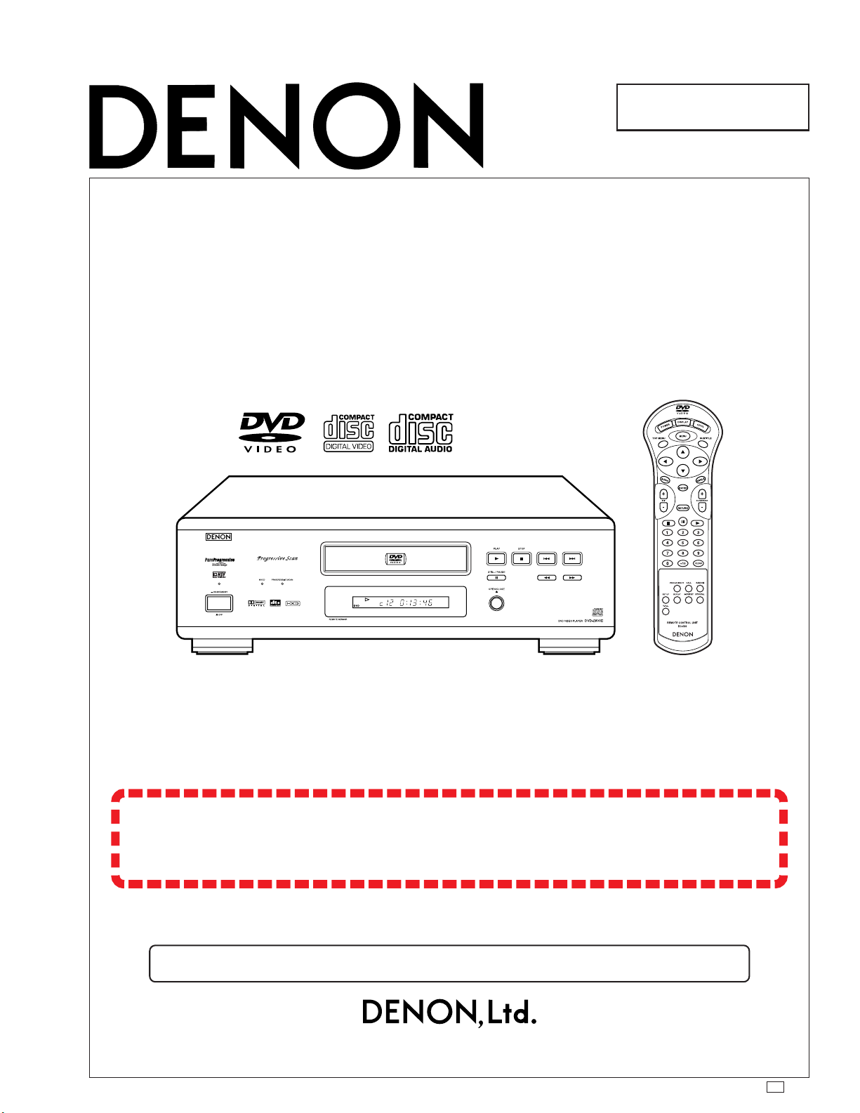
Denon DVD-2800MK2 Service Manual
SERVICE MANUAL
For U.S.A., Canada &
Europe model
Digital Player
MODEL
DVD VIDEO PLAYER
DVD-2800
II
This service manual is composed of only pages whose contents are different
from those for the model DVD-2800. For servicing, refer to the previously
issued service manual of DVD-2800 (X0111) at the same time.
Some illustrations using in this service manual are slightly different from the actual set.
16-11, YUSHIMA 3-CHOME, BUNKYOU-KU, TOKYO 113-0034 JAPAN
Telephone: 03 (3837) 5321
X0143 NC 0205
DVD-2800II
SAFETY PRECAUTIONS
The following check should be performed for the continued protection of the customer and service technician.
LEAKAGE CURRENT CHECK
Before returning the unit to the customer, make sure you make either (1) a leakage current check or (2) a line to chassis
resistance check. If the leakage current exceeds 0.5 milliamps, or if the resistance from chassis to either side of the
power cord is less than 460 kohms, the unit is defective.
SPECIFICATIONS
Signal System: NTSC/PAL
Applicable Discs: (1) DVD/Video discs
1-layer 12 cm single-sided discs, 2-layer 12 cm single-sided discs,
2-layer 12 cm double-sided discs (1 layer per side)
1-layer 8 cm single-sided discs, 2-layer 8 cm single-sided discs,
2-layer 8 cm double-sided discs (1 layer per side)
(2) Compact discs (CD-DA, Video CD)
12 cm discs, 8 cm discs
S-Video Output: Y output level: 1 Vp-p (75 Ω/ohms)
C output level: 0.286 Vp-p (For U.S.A. & Canada model)
0.3 Vp-p (For Europe model)
Output connectors: S connectors, 1 set
AV 1 connector, 1 set (For Europe model)
Video Output: Output level: 1 Vp-p (75 Ω/ohms)
Output connector: Pin-plug jacks, 1 set
AV 1 connector, 1 set (For Europe model)
Component Output: Y output level: 1 Vp-p (75 Ω/ohms)
B output level: 0.648 Vp-p (75 Ω/ohms) (For U.S.A. & Canada model)
C
0.7 Vp-p (75 Ω/ohms) (For Europe model)
R output level: 0.648 Vp-p (75 Ω/ohms) (For U.S.A. & Canada model)
C
0.7 Vp-p (75 Ω/ohms) (For Europe model)
Output connector: Pin jack, 1 set
RGB Output: Output level: 0.7 Vp-p (75 Ω/ohms) (For Europe model)
Output connector: AV 1 connector, 1 set (For Europe model)
Audio Output: Output level: 2 Vrms, 1 set
Audio Output Properties: (1) Frequency response
1
DVDs (linear PCM) : 2 Hz to 22 kHz (48 kHz sampling)
: 2 Hz to 44 kHz (96 kHz sampling)
2
CDs : 2 Hz to 20 kHz
(2) S/N ratio
1
DVDs : 115 dB
2
CDs : 115 dB
(3) Total harmonic distortion
1
DVDs : 0.0025 % (For Europe model)
: 0.0020 % (For U.S.A. & Canada model)
2
CDs : 0.0025 % (For Europe model)
: 0.0020 % (For U.S.A. & Canada model)
(4) Dynamic range
1
DVDs : 108 dB
2
CDs : 100 dB
Digital Audio Output: Optical digital output : Optical connector, 1 set
Coaxial digital output : Pin jack, 1 set
Power Supply: AC 120 V, 60 Hz (For U.S.A. & Canada model)
AC 230 V, 50 Hz (For Europe model)
Power Consumption: 22 W (For U.S.A. & Canada model)
18 W (For Europe model)
Maximum External Dimensions: 434 (W) × 132 (H) × 339 (D) mm (including protruding parts)
Mass: 6.5 kg
Remote Control Unit: RC-546
Type: Infrared pulse
Power Supply: DC 3 V, 2 "AAA" /R03 batteries
∗ Design and specifications are subject to change without notice in the course of product improvement.
2
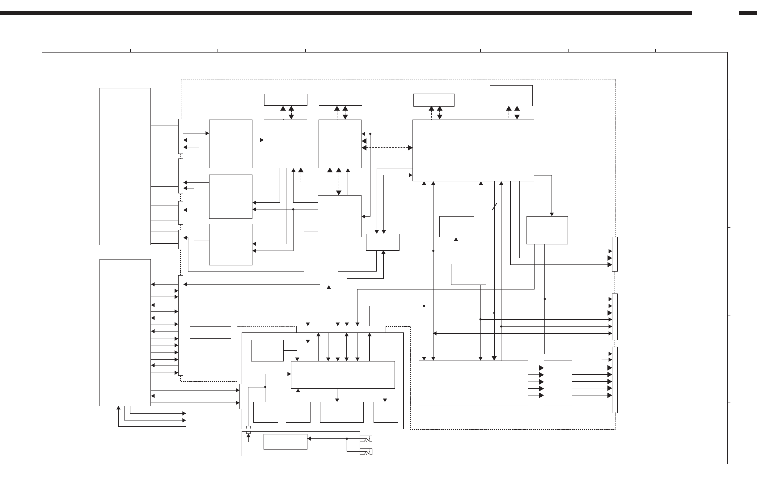
BLOCK DIAGRAMS
DVD DRIVE
MECHA
UNIT
FRONTEND
PROCESSOR
[TA1293F]
4ch MOTOR
DRIVER
[BA5952FP]
SPINDLE
MOTOR
DRIVER
[AN8471]
4M DRAM 4M DRAM
DISC SERVO
PROCESSOR
[TC9453F]
ATAPI
INTERFACE
DVD DECODER
[TC9469BF]
DRIVE
CONTROL
m
-COM
[TMP95CW64F]
POWER
SWITCHING
UNIT
GU-3340-2
+3.7V REG.
+3.3V[D1]REG.
[TC7WT125]
DVD PROCESSOR
[ES4408]
16M SDRAM x2
8M FLASH ROM
[HY29F080T]
E2PROM
[S24C01B]
I/O EXPANDER
[HCT273]
27MHz
OSC
BUFFER
AMP
VIDEO ENCODER
[ADV7172]
FRONT
m
-COM & FL DRIVER
[MN101C35D]
RESET
[MN1382]
REMO
CON
KEY
FLT
[HNV-13SM10]
LED
24P FFC
15P FFC
5P PH
3P PH
+5V[USW]
+5V[V]
+5V[D1]
GND[D1]
GND[V]
+5V[A]
GND[A]
+12V[A]
-12V[A]
+12V[M]
+5V[D2]
GND[D2]
+3.3V[D3]
GND[A]
-12V[A]
+12V[A]
VEE
FL+
FL-
96k,DEEM,/DFRES
TSDO,TWS,TBCK,MCLK
SPDIF
PROG/INT
/RST
YVU0~7
27M
HSYNC,VSYNC
SDA,SCL
VIDCNTL1,2,RGB-H
+5V[V]
G/Y
B/Cb
R/Cr
Y
C
HSYNC
VSYNC
8
LD8~15
/RST
HRESET
DMO,TRD
DMO
DATA
CS,CLK
ON/ST
PDET
(+5V[D])
/DFRES
/RST
/RST
I C BUS
2
DISP PWB UNIT
GU-3341
AUDIO PWB UNIT
GU-3340-1
MAIN PWB UNIT GU-3333
VIDEO PWB UNIT
GU-3441
VIDEO PWB UNIT
GU-3441
AUDIO PWB UNIT
GU-3340-1
DVD-2800II Block Diagram (1/2)
PRE AMP
CXA1511M
W. REM UNIT
GU-3341-4
IN
OUT
DVD-2800II
1
32
4
5678
A
B
C
D
E
3
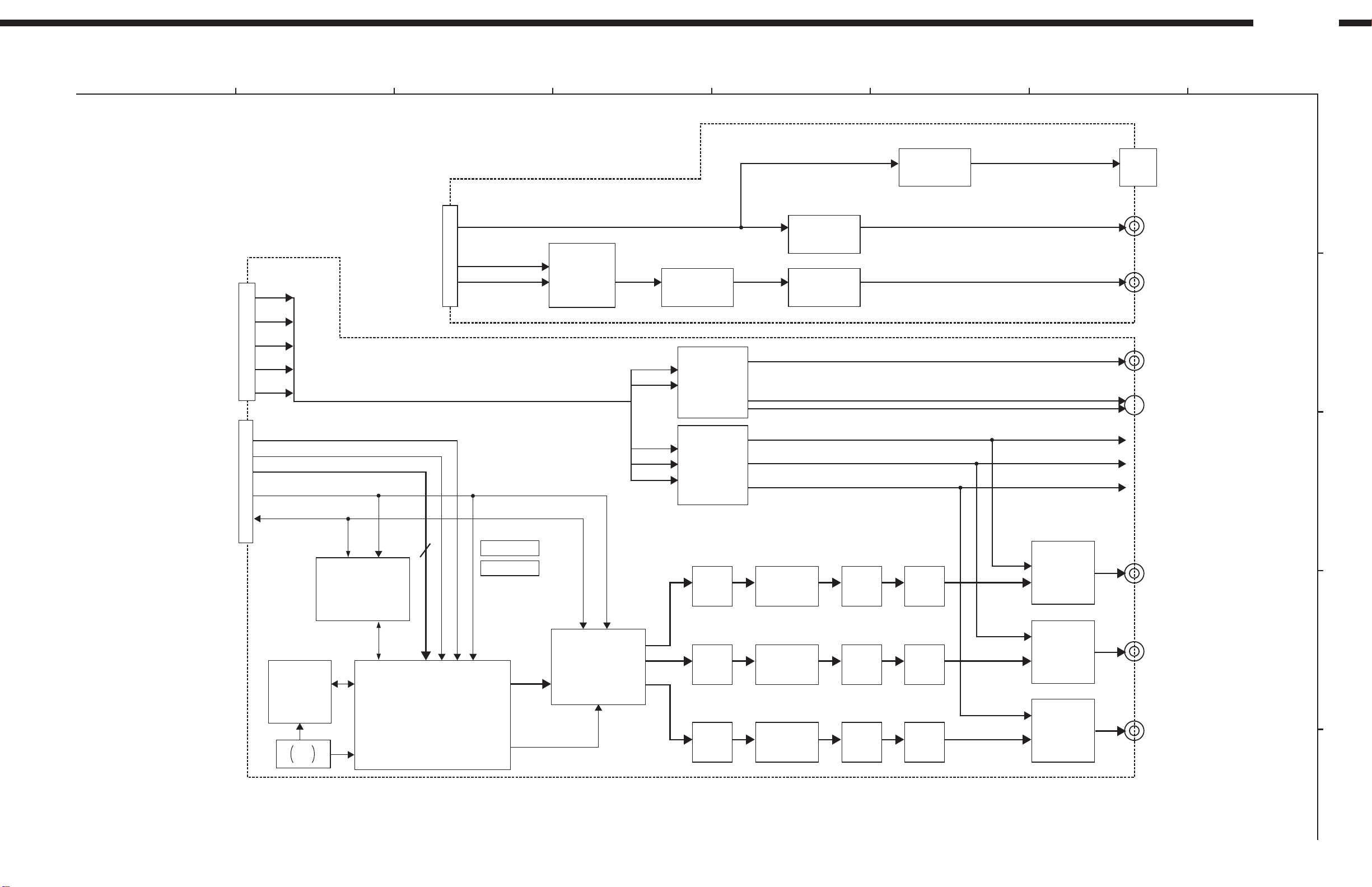
DVD-2800II
MAIN PWB
UNIT
GU-3333
Y
C
G/Y
B/CB
R/CR
MAIN PWB
UNIT
GU-3333
HSYNC,YSYNC
27M
YUV0~7
/RST
SDA,SCL
I C
2
8
I C
2
YCBCR
/RGB
HSYNC(P)
VSYNC(P)
PR
CR
PB
CB
Yp
Yi
R/CR
B/CB
G/Y
C
Y
V
OPTICAL
OUT
COAXIAL
OUT
AUDIO
OUT
VIDEO
OUT
Y OUT
PB/CB
OUT
PR/CR
OUT
MAIN PWB
UNIT
GU-3333
VIDEO PWB UNIT GU-3441
AUDIO PWB UNIT GU-3340-1
OPTICAL
PULSE TRANS
AUDIO AMPAUDIO AMP
AUDIO DAC
[AD1854K]
VIDEO FILTER
& DRIVER II
[ML6427]
VIDEO FILTER
& DRIVER I
[ML6427]
I/P CONTROL
m COM
[PIC18LC242]
64M
SD-RAM
72M
OSC
I/P
CONVERTER
[SiI504]
VIDEO DAC
[ADV7300]
I/V
&
BUFFER
I/V
&
BUFFER
I/V
&
BUFFER
Y
FILTER
PB
FILTER
PR
FILTER
VR
&
BUFFER
VR
&
BUFFER
VR
&
BUFFER
DRIVER
DRIVER
DRIVER
VIDEO
SELECTOR
(RELAY)
VIDEO
SELECTOR
(RELAY)
VIDEO
SELECTOR
(RELAY)
S-VIDEO
OUT
DVD-2800II Block Diagram (2/2)
+2.5V REG.
+1.8V REG.
1 5678
32
4
A
B
C
D
E
4
SEMICONDUCTORS
IC’s
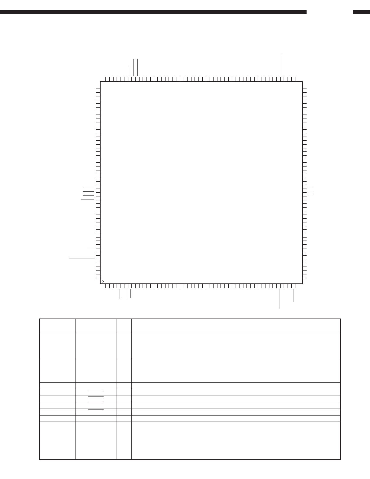
SiI504CM208 (IC701)
HostAddr5
HostAddr4
HostAddr3
156
155
HostAddr6
HostAddr7
HostMode
VDDCore
HostClk
HostData15\VidlnData19
HostData14\VidlnData18
HostData13\VidlnData17
HostData12\VidlnData16
HostData11\VidlnData15
HostData10\VidlnData14
GNDCore
GNDCore
VDDCore
HostData9\VidlnData13
HostData8\VidlnData12
RSVD
HostData7\VS
HostData6\HS
HostData5
HostData4
HostData3
HostData2
HostData1
HostData0
VDDIO
GNDIO
Det32PD
Det22PD
DetVideo
DeintDone
MemAddr12
VDDIO
GNDIO
SDOut
WSOut
SCKOut
VDDIO
SDIn
WSIn
SCKIn
GNDIO
VDDCore
Reset
Test0
Test1
BypPLLClk54_72M
Clk54_72M
VDDCore
GNDCore
ARTN
AVDD
154
157
158
159
160
161
162
163
164
165
166
167
168
169
170
171
172
173
174
175
176
177
178
179
180
181
182
183
184
185
186
187
188
189
190
191
192
193
194
195
196
197
198
199
200
201
202
203
204
205
206
207
208
123456789101112131415161718192021222324252627282930313233343536373839404142434445464748495051
DVD-2800II
HostAddr2
HostAddr1
HostAddr0
GNDCore
HostCS
HostRd_SDA
HostWr_SCL
VDDCore
VidlnClk
GNDIO
VidlnData9
VidlnData8
VidlnData7
VidlnData6
VidlnData5
VidlnData4
VidlnData3
VidlnData2
VDDIO
ExtRefXtalIOut
ExtRefXtalIn
VDDIO
GNDIO
MemData16
MemData17
MemData18
MemData19
GNDIO
MemData20
MemData21
MemData22
MemData23
GNDIO
MemData31
MemData30
GNDIO
VDDIO
MemData29
MemData28
GNDIO
MemData27
MemData26
MemData25
MemData24
MemData15
BypPLLMemClk
GNDCore
VDDCore
RSVD
153
152
151
150
149
148
147
146
145
144
143
142
141
140
139
138
137
136
135
134
133
132
131
130
129
128
127
126
125
124
123
122
121
120
119
118
117
116
115
114
113
112
111
110
109
108
107
106
105
RSVD
104
RSVD
103
GNDCore
102
MemClk
101
GNDCore
100
VDDCore
99
MemData14
98
MemData13
97
MemData12
96
MemData11
95
MemData10
94
GNDIO
93
MemData9
92
MemData8
91
PuPdDis
90
VDDIO
89
MemData0
88
MemData1
87
MemData2
86
GNDIO
85
MemData3
84
MemData4
83
MemData5
TOP VIEW
82
MemData6
81
MemData7
80
GNDIO
79
DQM
78
WE
77
CAS
76
RAS
75
VDDIO
74
VDDIO
73
GNDIO
72
RSVD
71
MemAddr11
70
MemAddr10
69
MemAddr9
68
MemAddr8
67
GNDIO
66
MemAddr7
65
MemAddr6
64
MemAddr5
63
MemAddr4
62
GNDIO
61
MemAddr0
60
MemAddr1
59
MemAddr2
58
MemAddr3
57
VDDCore
56
GNDCore
55
RSVD
54
RSVD
53
52
RSVD
VDDCore
GNDCore
LCDPwrEn
CBIank
CSync
VSync
HSync
Blue_Cb0
Blue_Cb1
Blue_Cb2
Blue_Cb3
Blue_Cb4
GNDIO
Blue_Cb5
VDDIO
Blue_Cb6
Blue_Cb7
Blue_Cb8
GNDIO
Blue_Cb9
VDDIO
Green_Y0
Green_Y1
Green_Y2
Green_Y3
Green_Y4
Green_Y5
GNDIO
Red_Cr0
Red_Cr1
Red_Cr2
Red_Cr3
Red_Cr4
Red_Cr5
Green_Y6
Green_Y7
Green_Y8
Green_Y9
GNDCore
SiI504CM208 Terminal Function
FunctionI/OPin No. Pin Name
2, 41, 51, 56,
99, 106, 146,
160, 168, 199,
205
3, 40, 47, 50,
55, 100, 102,
107, 150, 162,
167, 206
4 LCDPwrEn Out LCD Power Enable
5 CBlank Out Composite Blank
6 CSync Out Composite Sync
7 VSync Out Vertical Sync
8 HSync Out Horizontal Sync
9~14, 17~20 Blue_Cb[9:0] Out Blue Data (RGB output mode); Cb Data (YCrCb output mode)
15, 21, 33, 61,
66, 72, 79, 85,
93, 114, 118,
121, 126, 131,
144, 183, 190,
198
VDDCore Pwr 1.8V Core Power.
GNDCore Pwr Digital Ground for Core Power.
GNDIO Pwr Digital Ground for I/O Power.
Red_Cr6
Red_Cr7
Red_Cr8
VDDCore
Clk48M
Red_Cr9
VidOutClk
GNDCore
BypPLLClk48M
VDDCore
GNDCore
ExtRefSel
5
DVD-2800II
Pin No. Pin Name
16, 26, 73, 74,
89, 117, 132,
135, 182, 189,
194
22~25, 27~32 Green_Y[9:0] Out Green Data (RGB output mode); Y Data (YCrCb output mode)
34~39, 42~45 Red_Cr[9:0] Out Red Data (RGB output mode); Cr Data (YCrCb output mode)
46 VidOutClk Out Video Output Clock, 36, 27 or 24 MHZ
48 BypPLLClk48M In Bypass PLL for Clk48M.
49 Clk48M InOut 48 MHz Clock.
52 ExtRefSel In External APLL Reference Select.
57~60, 62~65,
67~70, 188
75 RAS Out SDRAM Row Address Strobe.
76 CAS Out SDRAM Column Address Strobe.
77 WE Out SDRAM Write Enable.
78 DQM Out SDRAM Data Mask.
80~84, 86~88,
91, 92, 94~98,
109, 110~113,
115, 116, 119,
120, 122~125,
127~130
90 PuPdDis In Internal pullup and pulldown disable test function.
101 MemClk InOut SDRAM Clock.
108 BypPLLMemClk In Bypass PLL for MemClk.
133 ExtRefXtalIn In External APLL Reference Crystal/oscillator Input.
134 ExtRefXtalOut Out External APLL Reference Crystal Output.
136~143 VidlnData[9:2] In Multiplexed Video Input Data; Y Video Input Data.
145 VidlnClk In Video Input Clock, 27.0 MHz
147 HostWr_SCL In 186-Compatible Write when HostMode=0. Serial Clock when HostMode=1.
148 HostRd_SDA InOut 186-Compatible Read when HostMode=0. Serial Data when HostMode=1.
149 HostCS In
151~158 HostAddr[7:0] In 186-Compatible Address when HostMode=0. No connect when HostMode=1.
159 HostMode In Serial Host Interface when HostMode=1. 186-compatible host interface when HostMode=0.
161 HostClk InOut 186-Compatible Clock when HostMode=0. No connect when HostMode=1.
163~166, HostData[15:8]
169~172 (VidInData[19:2])
174 HostData[7](VS) InOut 186-Compatible Data when HostMode=0. Vertical sync input when HostMode=1.
175 HostData[6](HS) InOut 186-Compatible Data when HostMode=0. Horizontal sync input when HostMode=1.
176~181 HostData[5:0] InOut 186-Compatible Data when HostMode=0. No connect when HostMode=1.
184 Det32PD Out 3:2 Pulldown Sequence Detected.
185 Det22PD Out 2:2 Pulldown Sequence Detected.
186 DetVideo Out Interlaced Video Sequence Detected.
187 DeintDone Out Deinterlace processing complete for current field period.
191 SDOut Out Serial Digital Audio Output Data.
192 WSOut Out Serial Digital Audio Output Word Select.
193 SCKOut Out Serial Digital Audio Output Clock.
195 SDIn In Serial Digital Audio Input Data.
196 WSIn In Serial Digital Audio Input Word Select.
197 SCKIn In Serial Digital Audio Input Clock.
200 Reset In Hardware Reset.
201, 202 Test[1:0] In Production hardware test support.
203
204 Clk54_72M InOut 54 or 72 MHz Clock.
207 ARTN Pwr Analog Return for PLLs.
208 AVDD Pwr 1.8V Analog Power for PLL.
VDDIO Pwr 3.3V I/O Power.
MemAddr[12:0] InOut SDRAM Address when an output. Configuration at reset when an input.
MemData[31:0] InOut SDRAM Data.
186-Compatible Chip Select when HostMode=0.
When HostMode=1, must be tied to VDD or pulled up to VDD.
InOut 186-Compatible Data when HostMode=0. Chroma video input data when HostMode=1.
BypPLLClk54_72M
In Bypass PLL for Clk54_72M.
FunctionI/O
6
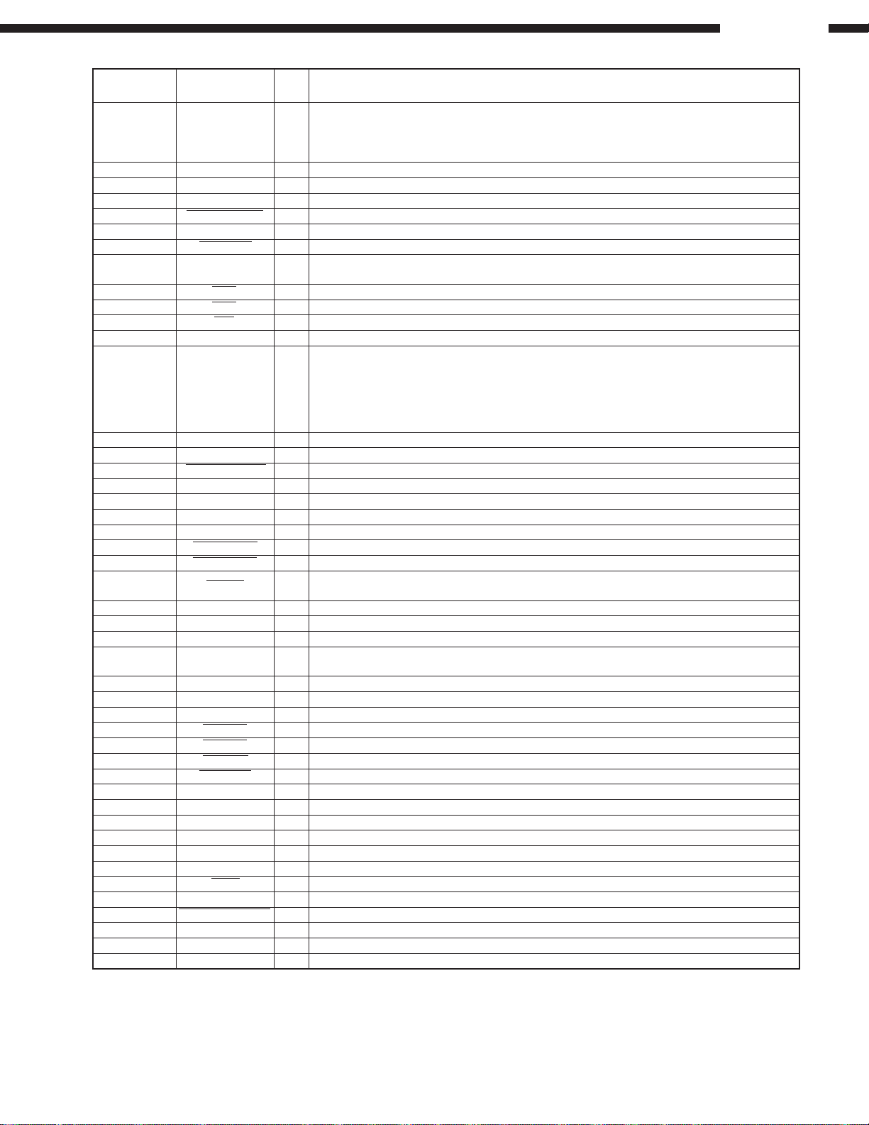
ADV7300 (IC706)
ADV7300 Terminal Function
VDD_IO
VDD
DGND
GND_IO
CLKIN_BS9S8S7S6S5DGND
646362616059585756555453525150
1
Y0
2
Y1
3
Y2
4
Y3
5
Y4
6
Y5
7
Y6
8
Y7
9
10
11
Y8
12
Y9
13
C0
14
C1
15
C2
16
171819202122232425262728293031
C3
TOP VIEW
C4
SPI/I2C
ALSB_SO
SDA_CLKSP
SCLK_SI
P_HSYNC
VDDS4S3S2S1
C5C6C7C8C9
P_BLANK
P_VSYNC
S0
S_VSYNC
S_HSYNC
49
32
CLKIN_A
RTC_SCR_TR
48
47
46
45
44
43
42
41
40
39
38
37
36
35
34
33
S_BLANK
R
SET 1
VREF
COMP1
DAC A
DAC B
DAC C
VAA
AGND
DAC D
DAC E
DAC F
COMP2
R
SET 2
EXT_LF
RESET
DVD-2800II
Pin No. Pin Name
FunctionI/O
1VDD_IO P Digital power supply.
2~9, 12, 13 Y9-0 I 10-Bit Progressive scan/ HDTV input port for Y data.
10, 56 VDD P Digital power supply.
11, 57 DGND G Digital Ground
14~18, 26~30 C9-0 I 10-Bit Progressive scan/ HDTV input port for CrCb color data in 4:2:2 input mode.
When this input pin is brought low, the ADV7300 interfaces over the SPI port and uses this
19 SPI/I2C I input as part of the 4 wire SPI interface. When this input pin is tied high [VDD_IO], the ADV7300
interfaces over the I2C port.
20 ALSB_SO I/O Multifunctional pin.
21 SDA_CLKSP I/O Multifunctional pin.
22 SCLK_SI I Multifunctional input.
23 P_HSYNC I
24 P_VSYNC I
Video Horizontal Sync Control Signal for HD sync in simultaneous SD/HD mode
and HD only mode.
Video Vertical Sync Control Signal for HD sync in simultaneous SD/HD mode
and HD only mode.
25 P_BLANK I Video Blanking Control Signal for HD sync in simultaneous SD/HD mode and HD only mode.
31 RTC_SCR_TR I Multifunctional input.
32 CLKIN_A I Pixel Clock Input for HD only or SD only modes.
33 RESET I
This input resets the on-chip timing generator and sets the ADV7300 into Default Register
setting. Reset is an active low signal.
34 EXT_LF I External Loop filter for the internal PLL.
35, 47 RSET1,2 I
A1520 Ohms resistor must be connected from this pin to AGND and is used to control the
amplitudes of the DAC outputs.
36,45 COMP O Compensation Pin for DACs.
37 DAC F O
38 DAC E O
39 DAC D O
In SD only mode: Chroma/RED/V analog output.
In HD only mode and simultaneus HD/SD: Pb/ BLUE (HD) analog output.
In SD only mode: Luma/BLUE/U analog output.
In HD only mode and simultaneus HD/SD: Pr/ RED (HD) analog output.
In SD only mode: CVBS/GREEN/Y analog output.
In HD only mode and simultaneus HD/SD: Y/ GREEN (HD) analog output.
40 AGND G Analog Ground
41 VAA P Analog power supply.
42 DAC C O Chroma/ RED/ V SD analog output.
43 DAC B O Luma/ BLUE/ U SD analog output.
44 DAC A O CVBS/ GREEN/ Y SD analog output.
46 VREF I/O Optional External Voltage Reference Input for DACs or Voltage Reference Output (1.235V).
48 S_BLANK I/O Video Blanking Control Signal for SD.
49 S_VSYNC I/O Video Vertical Sync Control Signal for SD.
50 S_HSYNC I/O Video Horizontal Control Signal for SD.
51~55, 58~62 S9-S0 I
10-Bit Standard Definition input port. Or Progressive Scan/ HDTV input port for
Cr [Red/V] color data in 4:4:4 input mode.
63 CLKIN_B I Pixel Clock Input.
64 GND_IO G Digital Ground
7
PIC18LC242-I/SO (IC703)
DVD-2800II
MCLR
RA0
RA1
RA2
RA3
RA4
RA5
V
OSC1
OSC2
RC0
RC1
RC2
RC3
1
2
3
4
5
6
7
SS
TOP VIEW
8
9
10
11
12
13
14
28
27
26
25
24
23
22
21
20
19
18
17
16
15
RB7
RB6
RB5
RB4
RB3
RB2
RB1
INT0
V
DD
V
SS
RC7
RC6
RC5
RC4
PIC18LC242-I/SO Terminal Function
Pin No. Pin Name
1 MCLR I Master Clear (Reset) input. This pin is an active low RESET to the device.
2 RA0 I/O Digital I/O.
3 RA1 I/O Digital I/O.
4 RA2 I/O Digital I/O.
5 RA3 I/O Digital I/O.
6 RA4 I/O Digital I/O. Open drain when configured as output.
7 RA5 I/O Digital I/O.
8VSS P Ground reference for logic and I/O pins.
9 OSC1 I
Oscillator crystal input or external clock source input.
ST buffer when configured in RC mode. CMOS otherwise.
10 OSC2 O Oscillator crystal output. Connects to crystal or resonator in Crystal Oscillator mode.
11 RC0 I/O Digital I/O.
12 RC1 I/O Digital I/O.
13 RC2 I/O Digital I/O.
14 RC3 I/O Digital I/O.
15 RC4 I/O Digital I/O.
16 RC5 I/O Digital I/O.
17 RC6 I/O Digital I/O.
18 RC7 I/O Digital I/O.
19 VSS P Ground reference for logic and I/O pins.
20 VDD P Positive supply for logic and I/O pins.
21 INT0 I External Interrupt 0.
22 RB1 I/O Digital I/O.
23 RB2 I/O Digital I/O.
24 RB3 I/O Digital I/O.
25 RB4 I/O Digital I/O. Interrupt-on-change pin.
26 RB5 I/O Digital I/O. Interrupt-on-change pin.
27 RB6 I/O Digital I/O. Interrupt-on-change pin. ICSP programming clock.
28 RB7 I/O Digital I/O. Interrupt-on-change pin. ICSP programming data.
DescriptionI/O
Legend: O=Output
I=Input
P=Power
8
T
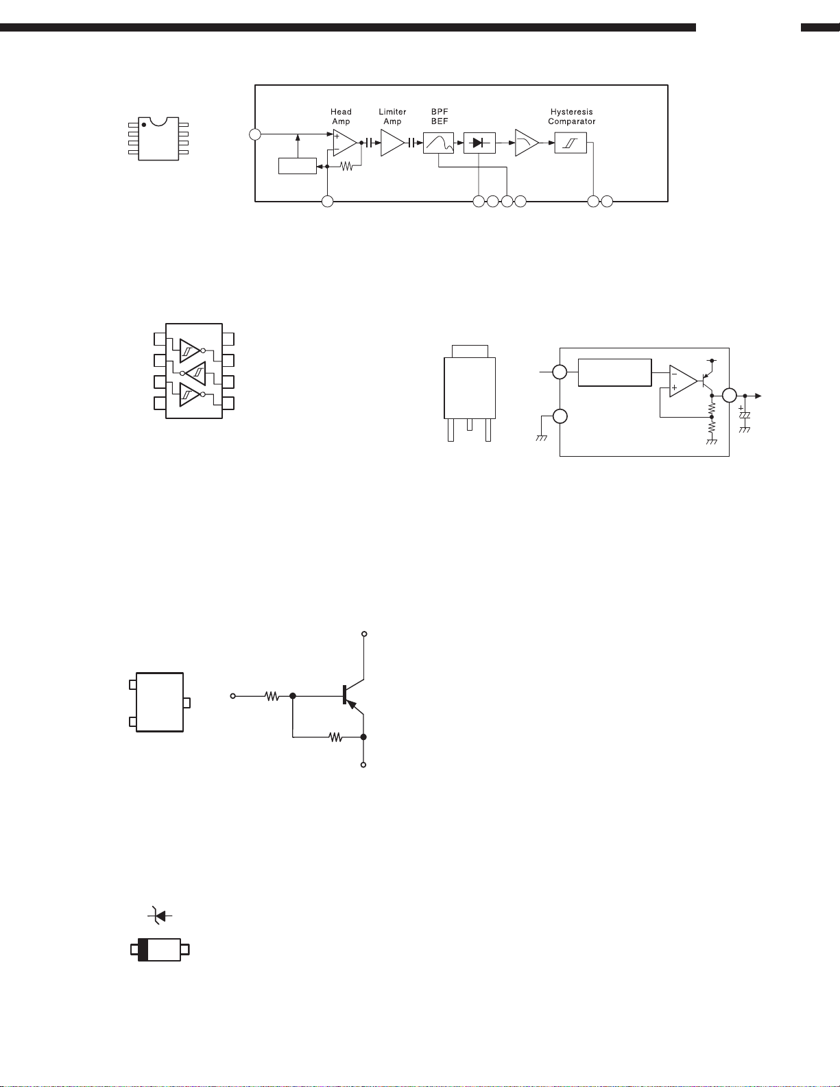
CXA1511M (IC510)
DVD-2800II
1
TOP
VIEW
45
8
TC7W14F (IC707)
1A
1
3Y
2
3
2A
4
GND
Detector &
IN
1
ABLC
2 3 4 5 6 7 8
C1
Comparator
C2
GNDfoN.C.
Integrator
OUT Vcc
BA18BC0FP (IC710)
Vcc
8
1Y
7
6
3A
5
2Y
2
TOP
VIEW
Vcc
GND
1
REFERENCE
VOLTAGE
OUT
3
2
1
3
TRANSISTORS
DTA144EK
B
TOP
VIEW
C
E
DIODES
UDZS5.1B
C
47kohm /9
B
47kohm /9
E
OP VIEW
9
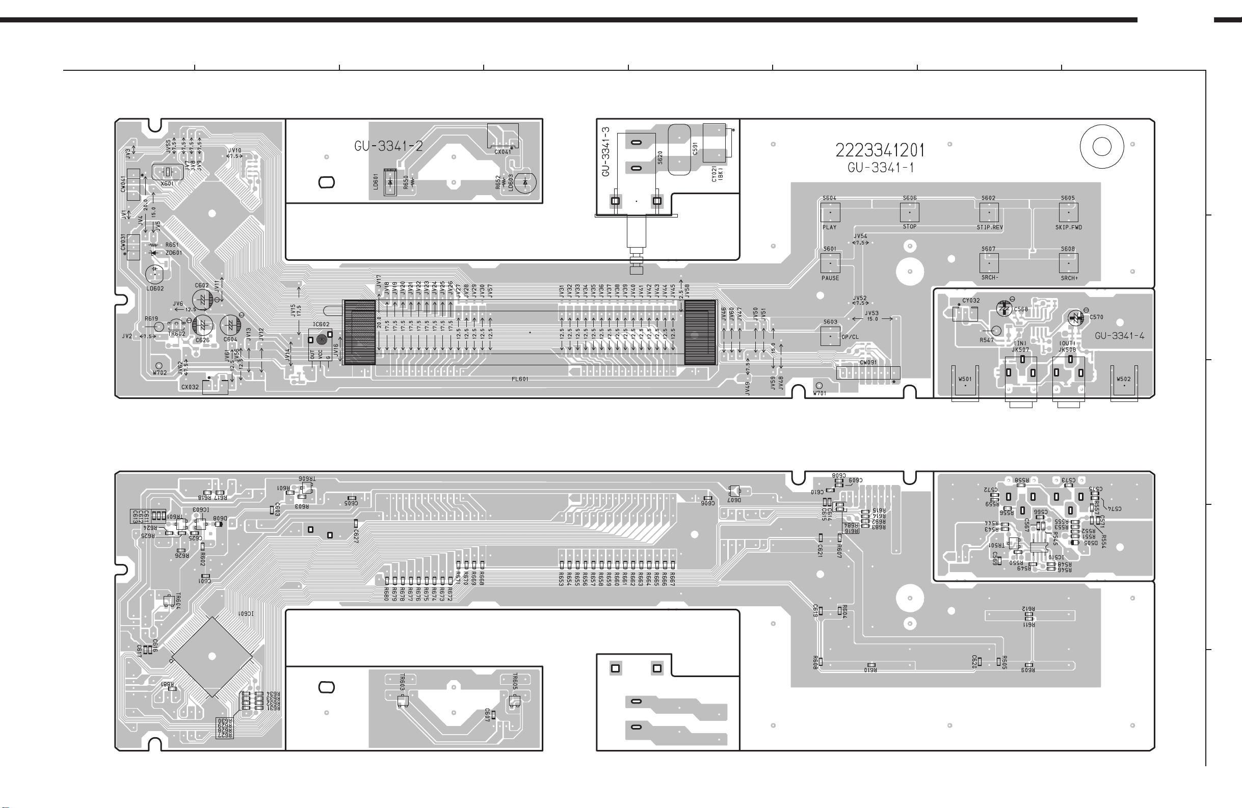
PRINTED WIRING BOARDS
DVD-2800II
1
DISPLAY P.W.B. UNIT
1
4
3
1
2
3
14
4
5
12
76
8
A
B
1 3
1
100
19
1
3
COMPONENT SIDE
C
1
4
8
5
D
75
76
51
50
25
26
E
FOIL SIDE
10
 Loading...