

Denon AVR-1513 User Manual
e
SERVICE MANUAL
MODEL JP E3 E2 EK EA E1C E1K CI
Ver. 1
AVR-1513
P P P
AV SURROUND RECEIVER
• For purposes of improvement, specications and design are subject to change without notice.
Please use this service manual with referring to the operating instructions without fail.
•
Some illustrations using in this service manual are slightly different from the actual set.
•
e
D&M Holdings Inc.
S0422-0V01DM/DG1202
Copyright 2012 D&M Holdings Inc. All rights reserved.
WARNING: Violators will be prosecuted to the maximum extent possible.

CONTENTS
ABOUT THIS MANUAL
What you can do with this manual ............................................3
Using Adobe Reader (Windows version) ..................................4
SAFETY PRECAUTIONS
NOTE FOR SCHEMATIC DIAGRAM
NOTE FOR PARTS LIST
TECHNICAL SPECIFICATIONS
DIMENSION
CAUTION IN SERVICING
Initializing AV SURROUND RECEIVER ....................................9
Service Jig ................................................................................9
DISASSEMBLY
1. FRONT PANEL ASSY .........................................................12
2. DIGITAL PCB ASSY ............................................................13
3. RADIATOR ASSY ................................................................14
4. POWER PCB ......................................................................15
5. REGULATOR PCB ..............................................................15
6. TRANS POWER ..................................................................15
SPECIAL MODE
Special mode setting button ....................................................16
1. µcom/DSP/OSD Version display mode ...............................17
WHEN THE MICROPROCESSOR IS
REPLACED WITH A NEW ONE
PROCEDURE FOR UPGRADING
THE VERSION OF THE FIRMWARE
1. Preparations ........................................................................18
2. UPDATE FIRMWARE ..........................................................23
3. Notice: .................................................................................42
Conrming the rmware’s number after upgraded ..................42
ADJUSTMENT
SURROUND MODES AND PARAMETERS
TROUBLE SHOOTING
1. POWER ...............................................................................47
2. Analog video ........................................................................48
3. HDMI/DVI ............................................................................49
4. AUDIO .................................................................................54
CLOCK FLOW & WAVE FORM IN DIGITAL BLOCK
ANALOG AUDIO/VIDEO BLOCK DIAGRAM
DIGITAL AUDIO/HDMI BLOCK DIAGRAM
POWER BLOCK DIAGRAM
LEVEL DIAGRAM
WIRING DIAGRAM
PRINTED WIRING BOARDS
MAIN .......................................................................................66
TUNER ....................................................................................68
POWER KNOB .......................................................................68
PORTABLE .............................................................................68
HEADPHONE .........................................................................68
USB .........................................................................................68
FOR HDMI FFC CABLE ..........................................................68
FRONT ....................................................................................69
DIGITAL ...................................................................................70
F-HDMI ....................................................................................72
POWER ...................................................................................72
REGULATOR ..........................................................................74
...............................................................................8
.........................................................................43
.............................................................3
..........................................................6
.........................................7
...........................................................7
................................................8
..........................................................9
........................................................................10
......................................................................16
.............................................18
.....................................18
............................44
............................................................47
.............57
.........................58
.............................59
....................................................60
....................................................................61
..................................................................65
...................................................66
SCHEMATIC DIAGRAMS
FRONT PART ..........................................................................76
POWER PART ........................................................................77
MAIN PART .............................................................................78
INPUT & VOLUME PART ........................................................79
VIDEO PART (PRE OUT-SUBWOOFER) ...............................80
DSP PART ...............................................................................81
MCU PART ..............................................................................82
HDMI PART .............................................................................83
FRONT-HDMI IN PART ...........................................................84
EXPLODED VIEW
PARTS LIST OF EXPLODED VIEW
PACKING VIEW
PARTS LIST OF PACKING & ACCESSORIES
SEMICONDUCTORS
1. IC's ......................................................................................92
2. FL DISPLAY.......................................................................111
PARTS LIST OF P.C.B. UNIT
FRONT PCB UNIT ASS'Y .....................................................113
POWER PCB UNIT ASS'Y .................................................... 116
MAIN PCB UNIT ASS'Y.........................................................118
DIGITAL PCB UNIT ASS'Y ....................................................123
.......................................................................90
........................................................76
....................................................................85
........................................87
.......................90
...............................................................92
................................................11 3
2
ABOUT THIS MANUAL
Read the following information before using the service manual.
What you can do with this manual
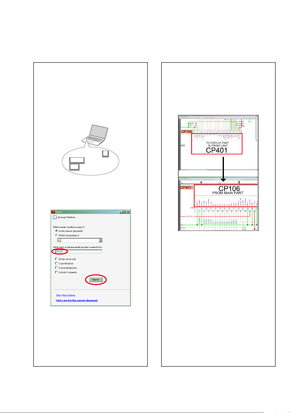
Search for a Ref. No. (phrase)
(Ctrl+Shift+F)
You can use the search function in Acrobat Reader to
search for a Ref. No. in schematic diagrams, printed
wiring board diagrams, block diagrams, and parts lists.
1.Press
2.Enter the Ref. No. you want to search for in the
Ctrl+Shift+F
on the keyboard.
• The Search window appears.
F
Shift
Ctrl
Search window, and then click the
• A list of search results appears.
Search
button.
Jump to the target of a schematic diagram
connector
Click the Ref. No. of the target connector in the red box
around a schematic diagram connector.
• The screen jumps to the target connector.
3.Click an item on the list.
• The screen jumps to the page for that item, and
the search phrase is displayed.
• Page magnification stays the same as before the
jump.
3

Using Adobe Reader (Windows version)
Add notes to this data (Sign)
The Sign function lets you add notes to the data in this
manual.
Save the le once you have nished adding notes.
[Example using Adobe Reader X]
On the "
View
" menu, click "
• The Sign pane appears.
[Example using Adobe Reader 9]
On the "
Document
" menu, click "
Sign
".
Sign
".
Magnify schematic / printed wiring board
diagrams - 1
(Ctrl+Space, mouse operation)
Ctrl+Space
Press
mouse to select the area you want to view.
• The selected area is magnied.
• When you want to move the area shown, hold down
Space
and drag the mouse.
• When you want to show a full page view, press
Ctrl+0
on the keyboard.
on the keyboard and drag the
0
Ctrl Space
Printamagniedpartofthemanual
The Properties dialog box and functions will vary depending on your printer.
1. Drag the mouse to magnify the part you want to print.
2. On the "
File
" menu, click "
3. Congure the following settings in the Print dialog box.
Print
".
• Properties
Click this button and check that the printer is set to a
suitable paper size.
• Pagetoprint
Select the following checkbox.
More Options
"
• PageSizing&Handling
Select the following checkbox.
"
Size
SizeOptions
" / "
Current View
" : "
" : "
Fit
"
"
4. Click the
Print
button to start printing.
4

Magnify schematic / printed wiring board
diagrams - 2
(Pan & Zoom function)
The Pan & Zoom function lets you see which part of a
magnied diagram is being shown in a separate window.
Magnify schematic / printed wiring board
diagrams - 3
(Loupe Tool function)
The Loupe Tool function lets you magnify a specific
part of a diagram in a separate window.
[Example using Adobe Reader X]
On the "
Pan & Zoom
"
• The Pan & Zoom window appears on the screen.
View
" menu, point to "
".
Zoom
", and then click
[Example using Adobe Reader X]
On the "
Loupe Tool
"
• The Loupe Tool window appears on the screen.
View
" menu, point to "
".
Zoom
", and then click
[Example using Adobe Reader 9]
On the "
then click "
Tools
" menu, point to "
Pan & Zoom Window
Select & Zoom
[Example using Adobe Reader 9]
", and
".
On the "
then click "
5
Tools
" menu, point to "
Loupe Tool Window
Select & Zoom
".
", and

SAFETY PRECAUTIONS
The following items should be checked for continued protection of the customer and the service technician.
LEAKAGE CURRENT CHECK
Before returning the set to the customer, be sure to carry out either (1) a leakage current check or (2) a line to chassis
resistance check. If the leakage current exceeds 0.5 milliamps, or if the resistance from chassis to either side of the
power cord is less than 460 kohms, the set is defective.
Be sure to test for leakage current with the AC plug in both polarities, in addition, when the set's power is in each state (on,
off and standby mode), if applicable.
CAUTION
Please heed the following cautions and instructions during servicing and
inspection.
◎Heed the cautions!
Cautions which are delicate in particular for servicing
are labeled on the cabinets, the parts and the chassis,
etc. Be sure to heed these cautions and the cautions
described in the handling instructions.
◎Cautions concerning electric shock!
(1) An AC voltage is impressed on this set, so if
you touch internal metal parts when the set is
energized, you may get an electric shock. Avoid
getting an electric shock, by using an isolating
transformer and wearing gloves when servicing
while the set is energized, or by unplugging the
power cord when replacing parts, for example.
(2) There are high voltage parts inside. Handle with
extra care when the set is energized.
◎ Caution concerning disassembly and
assembly!
Through great care is taken when parts were
manufactured from sheet metal, there may be burrs
on the edges of parts. The burrs could cause injury if
ngers are moved across them in some rare cases.
Wear gloves to protect your hands.
◎Use only designated parts!
The set's parts have specic safety properties (re
resistance, voltage resistance, etc.). Be sure to use
parts which have the same properties for replacement.
The burrs have the same properties. In particular, for
the important safety parts that are indicated by the z
mark on schematic diagrams and parts lists, be sure to
use the designated parts.
◎ Be sure to mount parts and arrange the wires
as they were originally placed!
For safety seasons, some parts use tapes, tubes or
other insulating materials, and some parts are mounted
away from the surface of printed circuit boards.
Care is also taken with the positions of the wires by
arranging them and using clamps to keep them away
from heating and high voltage parts, so be sure to set
everything back as it was originally placed.
◎Make a safety check after servicing!
Check that all screws, parts and wires removed or
disconnected when servicing have been put back in
their original positions, check that no serviced parts
have deteriorate the area around. Then make an
insulation check on the external metal connectors and
between the blades of the power plug, and otherwise
check that safety is ensured.
(Insulation check procedure)
Unplug the power cord from the power outlet,
disconnect the antenna, plugs, etc., and on the power.
Using a 500V insulation resistance tester, check that
the insulation resistance value between the inplug and
the externally exposed metal parts (antenna terminal,
headphones terminal, input terminal, etc.) is 1MΩ or
greater. If it is less, the set must be inspected and
repaired.
CAUTION
Concerning important safety
parts
Many of the electric and the structural parts used in
the set have special safety properties. In most cases
these properties are difcult to distinguish by sight, and
the use of replacement parts with higher ratings (rated
power and withstand voltage) does not necessarily
guarantee that safety performance will be preserved.
Parts with safety properties are indicated as shown
below on the wiring diagrams and the parts list in this
service manual. Be sure to replace them with the parts
which have the designated part number.
(1) Schematic diagrams ....... Indicated by the z mark.
(2) Parts lists .......Indicated by the z mark.
The use of parts other than the
designated parts could cause electric
shocks, res or other dangerous
situations.
6

NOTE FOR SCHEMATIC DIAGRAM
NOTE FOR PARTS LIST
WARNING:
Parts indicated by the z mark have critical characteristics. Use ONLY replacement parts recommended by the manufacturer.
CAUTION:
Before returning the set to the customer, be sure to carry out either (1) a leakage current check or (2) a line to chassis resistance check. If
the leakage current exceeds 0.5 milliamps, or if the resistance from chassis to either side of the power cord is less than 460 kohms, the set
is defective.
WARNING:
DO NOT return the set to the customer unless the problem is identied and remedied.
NOTICE:
ALL RESISTANCE VALUES IN OHM. k=1,000 OHM / M=1,000,000 OHM
ALL CAPACITANCE VALUES ARE EXPRESSED IN MICRO FARAD, UNLESS OTHERWISE INDICATED. P INDICATES MICRO-MICRO
FARAD. EACH VOLTAGE AND CURRENT ARE MEASURED AT NO SIGNAL INPUT CONDITION. CIRCUIT AND PARTS ARE SUBJECT
TO CHANGE WITHOUT PRIOR NOTICE.
NOTE FOR PARTS LIST
1.
Parts indicated by "nsp" on this table cannot be supplied.
2.
When ordering a part, make a clear distinction between "1" and "I" (i) to avoid mis-supplying.
3.
A part ordered without specifying its part number can not be supplied.
4.
Part indicated by "★" mark is not illustrated in the exploded view.
5.
General-purpose Carbon Film Resistor in the P.W.Board parts list. (Refer to the Schematic Diagram for those parts.)
6.
General-purpose Carbon Chip Resistors are not included are not included in the P.W.Board parts list.
(Refer to the Schematic Diagram for those parts.)
WARNING:
Parts indicated by the z mark have critical characteristics. Use ONLY replacement parts recommended by the manufacturer.
7
TECHNICAL SPECIFICATIONS
nAudio Section
• Poweramplier
Rated output :
Front :
75 W + 75 W (8 Ω, 20 Hz – 20 kHz with 0.08 % T.H.D.)
110 W + 110 W (6 Ω, 1 kHz with 0.7 % T.H.D.)
130W+130W(6Ω, JEITA)
Center :
75 W (8 Ω, 20 Hz – 20 kHz with 0.08 % T.H.D.)
110 W (6 Ω, 1 kHz with 0.7 % T.H.D.)
130W(6Ω, JEITA)
Surround :
75 W + 75 W (8 Ω, 20 Hz – 20 kHz with 0.08 % T.H.D.)
110 W + 110 W (6 Ω, 1 kHz with 0.7 % T.H.D.)
130W+130W(6Ω, JEITA)
Output connectors : 6 – 16 Ω
• Analog
Input sensitivity/Input impedance : 200 mV/47 kΩ
Frequency response: 10 Hz – 100 kHz — +1, –3 dB (DIRECT mode)
S/N : 98 dB (IHF–A weighted, DIRECT mode)
nVideo section
• Standard video connectors
Input/output level and impedance : 1 Vp-p, 75 Ω
Frequency response: 5 Hz – 10 MHz — 0, –3 dB
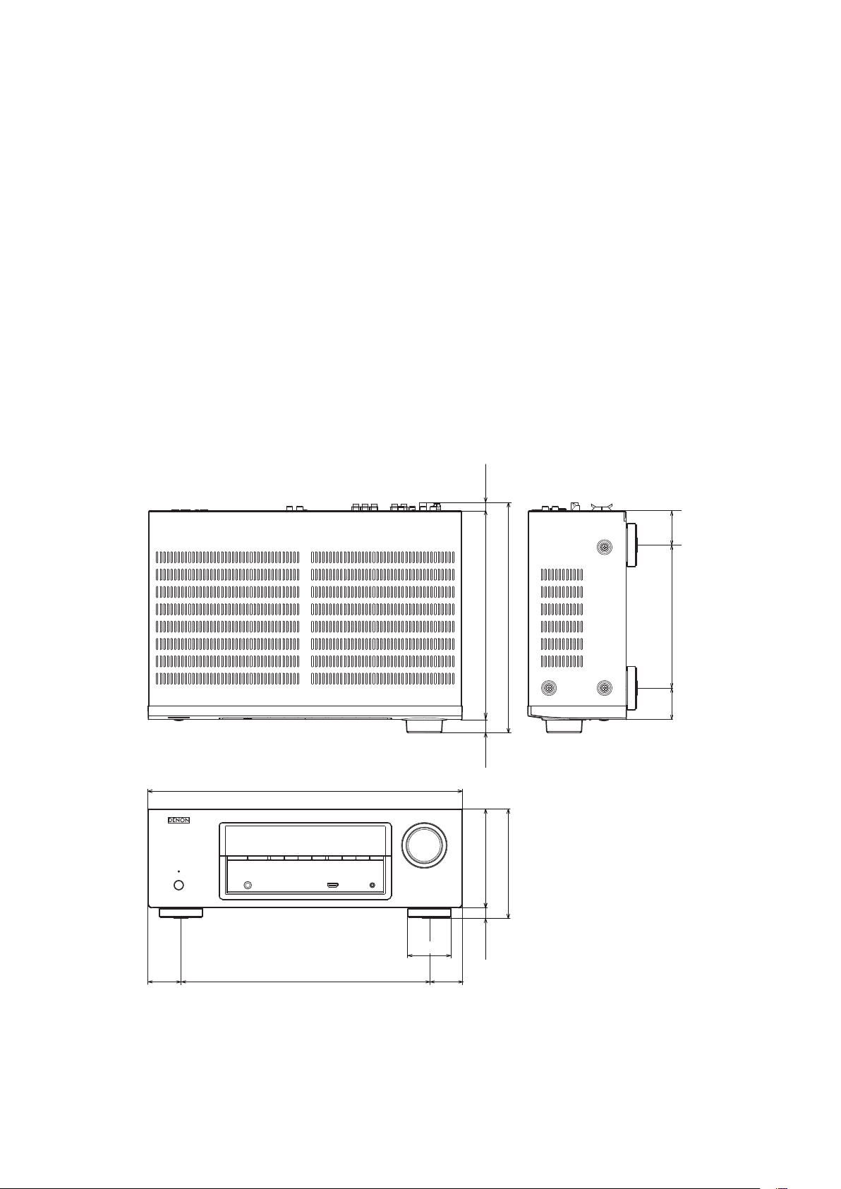
DIMENSION
nTuner section
[FM](Note: μV at 75 Ω, 0 dBf = 1 x 10
Receiving Range (for E3) :
[FM] 87.5 MHz – 107.9 MHz [AM]520 kHz – 1710 kHz
Receiving Range (for E2, E1C) :
[FM] 87.5 MHz – 108.0 MHz [AM]522 kHz – 1611 kHz
Usable Sensitivity :
[FM]1.2 μV (12.8 dBf) [AM]18 μV
50 dB Quieting Sensitivity :
[FM]MONO 2.8 μV (20.2 dBf)
S/N (IHF-A) :
[FM]MONO 70 dB (IHF–A weighted, DIRECT mode)
STEREO 67 dB (IHF–A weighted, DIRECT mode)
TotalharmonicDistortion(at1kHz):
[FM]MONO 0.7 %
STEREO 1.0 %
nGeneral
Power supply : (for E3) : AC 120 V, 60 Hz
(for E2) : AC 230 V, 50 Hz / 60Hz
(for E1C) : AC 220 V, 50 Hz
Power consumption : 330 W
0.5 W (Standby)
–15
W)
Weight : 7.8kg
434.0
60.0
344.045.0 45.0
288.5
18.5 12.0
136.0
15.0
319.0
151.0
198.043.5 47.0
8

CAUTION IN SERVICING
InitializingAVSURROUNDRECEIVER
AV SURROUND RECEIVER initialization should be performed when the μcom, peripheral parts of μcom, and Digital
PCB were replaced.
1. Turn off the power pressing X button.
2. Press X button while simultaneously while pressing SOURCE SELECT 0 and SOURCE SELECT 1 buttons.
3. Check that the entire display is ashing at intervals of about 1 second, and then release the 2 buttons.
The microprocessor will be initialized.
Note: • If step 3 fails, start over from step 1.
• All user settings will be lost and the factory setting will be recovered after the set is initialized.
So make sure to note down your setting beforehand for restoring after the initialization.
SOURCE SELECT 0
X
SOURCE SELECT 1
Service Jig
When you update the rmware, you can use the following
JIG (RS232C to internal connector conversion adapter).
Please order it from Denon Ofcial Service Distributor in your region if necessary.
8U-210100S : WRITING KIT : 1 Set
606050028012P : 7P FFC(1.0) L-240 : 1 Set
(Refer to "PROCEDURE FOR UPGRADING THE VERSION OF THE FIRMWARE".)
9
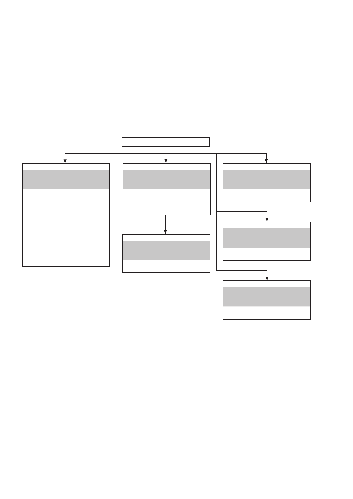
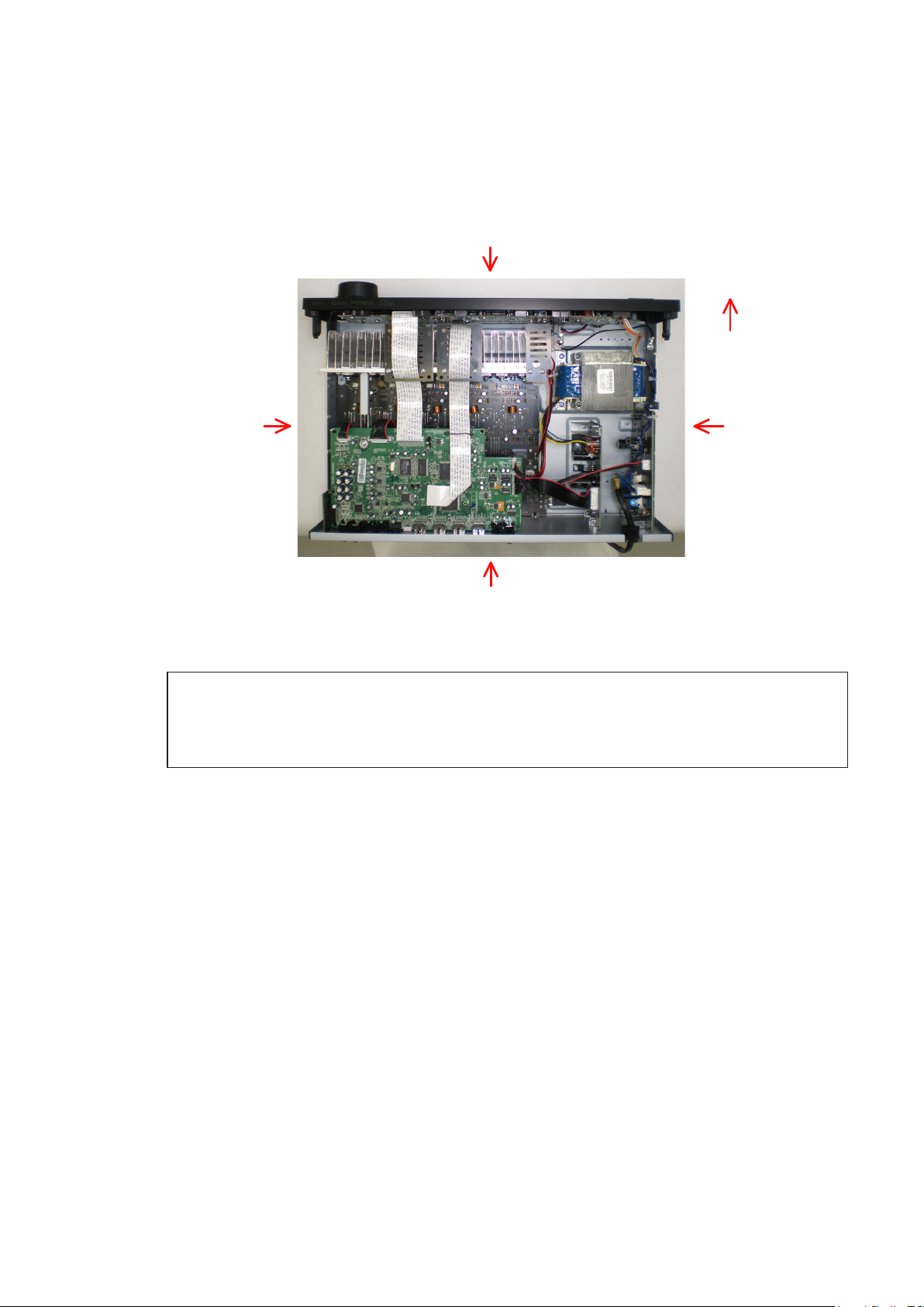
DISASSEMBLY
• Disassemble in order of the arrow in the following gure.
• In the case of the re-assembling, assemble it in order of the reverse of the following ow.
• In the case of the reassembling, observe "Caution concerning disassembly and assembly!".
• If wire bundles are untied or moved to perform adjustment or replace parts etc., be sure to rearrange them neatly as
they were originally bundled or placed afterward.
Otherwise, incorrect arrangement can be a cause of noise generation.
TOP CABINET
FRONT PANEL ASSY
"DISASSEMBLY
Refer to
1. FRONT PANEL ASSY"
"EXPLODED VIEW"
and
FRONT PCB
(Ref. No. of EXPLODED VIEW : C1-1)
POWER KNOB PCB
(Ref. No. of EXPLODED VIEW : C1-2)
HEADPHONE PCB
(Ref. No. of EXPLODED VIEW : C1-3)
PORTABLE PCB
(Ref. No. of EXPLODED VIEW : C1-4)
USB PCB
(Ref. No. of EXPLODED VIEW : C1-5)
F-HDMI PCB
(Ref. No. of EXPLODED VIEW : C3-2)
DIGITAL PCB ASSY
"DISASSEMBLY
Refer to
2. DIGITAL PCB ASSY"
"EXPLODED VIEW"
and
DIGITAL PCB
(Ref. No. of EXPLODED VIEW : C3-1)
TUNER PCB
(Ref. No. of EXPLODED VIEW : C2-5)
RADIATOR ASSY
"DISASSEMBLY
Refer to
3. RADIATOR ASSY"
"EXPLODED VIEW"
and
MAIN PCB
(Ref. No. of EXPLODED VIEW : C2-1)
POWER PCB
"DISASSEMBLY
Refer to
4. POWER PCB"
"EXPLODED VIEW"
and
POWER PCB
(Ref. No. of EXPLODED VIEW : C4-1)
REGULATOR PCB
"DISASSEMBLY
Refer to
5. REGULATOR PCB"
"EXPLODED VIEW"
and
REGULATOR PCB
(Ref. No. of EXPLODED VIEW : C4-2)
TRANS POWER
"DISASSEMBLY
Refer to
6. TRANS POWER"
"EXPLODED VIEW"
and
TRANS POWER
(Ref. No. of EXPLODED VIEW : C6 )
10
About the photos used for "descriptions of the DISASSEMBLY" section
• The shooting direction of each photograph used herein is indicated on the left side of the respective photograph as
"Shooting direction: ***". (*** : A,B,C,D)
• Refer to the diagram below about the shooting direction of each photograph.
• Photographs with no shooting direction indicated were taken from the top of the set.
The viewpoint of each photograph
(Shooting direction)
Shooting direction: B
[View from the top]
Note: • Before disassembling this unit, be sure to discharge the power line (the colored line in the
schematic diagram).
• FFC cables with one end disconnected should be insulated by using tapes, etc.
Front side
Shooting direction: DShooting direction: C
Shooting direction: A
11

1. FRONT PANEL ASSY
Proceeding :
(1) Remove the screws.
View from the bottom
(2) Remove the screws and disconnect the FFC.
CABINET TOP
FRONT PANEL ASSY
→
FRONT PANEL ASSY
FFC
(3) Disconnect the connector wires.
CN102
CN104
Please refer to "EXPLODED VIEW" for the disassembly method of each PCB included in FRONT PANEL ASSY.
12

2. DIGITAL PCB ASSY
Proceeding :
(1) Remove the screws.
Shooting direction: A
(2) Remove the screws.
Disconnect the connector wires and FFC then disconnect the TUNER PCB.
CN90
CABINET TOP
DIGITAL PCB ASSY
→
CN95
TUNER PCB
FFC
DIGITAL PCB
CN205
CN202
13

3. RADIATOR ASSY
Proceeding :
(1) Remove the screws.
Shooting direction: A
(2) Remove the screws then disconnect the connector wire.
Remove the RADIATOR ASSY from the CHASSIS BOTTOM.
MAIN PCB
CABINET TOP
DIGITAL PCB ASSY
→
RADIATOR ASSY
→
CN503
14

4. POWER PCB
Proceeding :
Please refer to "EXPLODED VIEW" for the disassembly method of POWER PCB.
CABINET TOP
POWER PCB
→
5. REGULATOR PCB
Proceeding :
Please refer to "EXPLODED VIEW" for the disassembly method of REGULATOR PCB.
CABINET TOP
REGULATOR PCB
→
6. TRANS POWER
Proceeding :
Please refer to "EXPLODED VIEW" for the disassembly method of TRANS POWER.
CABINET TOP
TRANS POWER
→
15
SPECIAL MODE
Special mode setting button
Press the
b
µcom/DSP/OSD Version display
mode
Initialization mode
Mode for switching tuner frequency
step
When power is turned on, pressing both buttons A and B at the same time for 3 seconds or more.
b
Select the video signal format STATUS
Mode for preventing remote control
acceptance
button to turn on the power while pressing both the button A and the button B at the same time.
X
Mode Button A Button B Contents
Firmware versions such as Main, DSP or OSD are displayed
STATUS DIMMER
SOURCE
SELECT
Mode Button A Button B Contents
0
DIMMER
ATUS DIMMER
ST
SOURCE
SELECT
SOURCE
SELECT
SOURCE
SELECT
in the FL display. Errors are displayed or when they occur.
(Refer to 17 page.)
Backup data initialization is carried out. (Refer to 9 page.)
1
---E2 model only---
Change tuner frequency step to AM9k/FM50kHz STEP or
1
AM:10k/FM:200kHz.
Select with the "SOURCE SELECT 0", "SOURCE SELECT
0
" and "STATUS" button change video format NTSC or PAL.
1
Operations using the remote control are rejected.
"REMOTE LOCK:ON" is displayed in FL display.
(Mode the cancellation: Execute the same button operations
as when performing setup.)
STATUSSOURCE SELECT 0
DIMMER
X
SOURCE SELECT 1
16
1. µcom/DSP/OSD Version display mode
1.1. Operationspecications
µcom/DSP/OSD version display mode:
When the set is started up in this mode, the version information is displayed.
Starting up:
Press the X button to turn on the power while pressing the "DIMMER" and "STATUS" buttons.
Now, press the "STATUS" button to the display the 2nd item information on the FL Display.
1.2. Display Order
Model destination information → w Main-µcom version → e DSP version → r OSD version
q
Display State
Model destination information
q
AVR-1513 E3 model
A V R 1 5 1 3 E 3
AVR-1513 E2 model
AVR-1513 E1C model
Main-µcom version
w
DSP version
e
OSD version
r
A V R 1 5 1 3 E 2
A V R 1 5 1 3 E 1 C
M a i n : * * . * *
D S P . * . * . *
O S D : * * . * *
Cleared of mode:
Press the X button to turn the power off.
1.3. Error display
See the following table for each "Error information" display and its contents (status).
Condition - State
DSP NG When DSP boot, executing DSP reset makes to becomes error.
DSP OK (No error display, version display only)
D S P E R R O R 0 1
17
WHEN THE MICROPROCESSOR IS REPLACED WITH A NEW ONE
When the U-PRO (Microprocessor) or the Flash ROM is replaced, conrm the following.
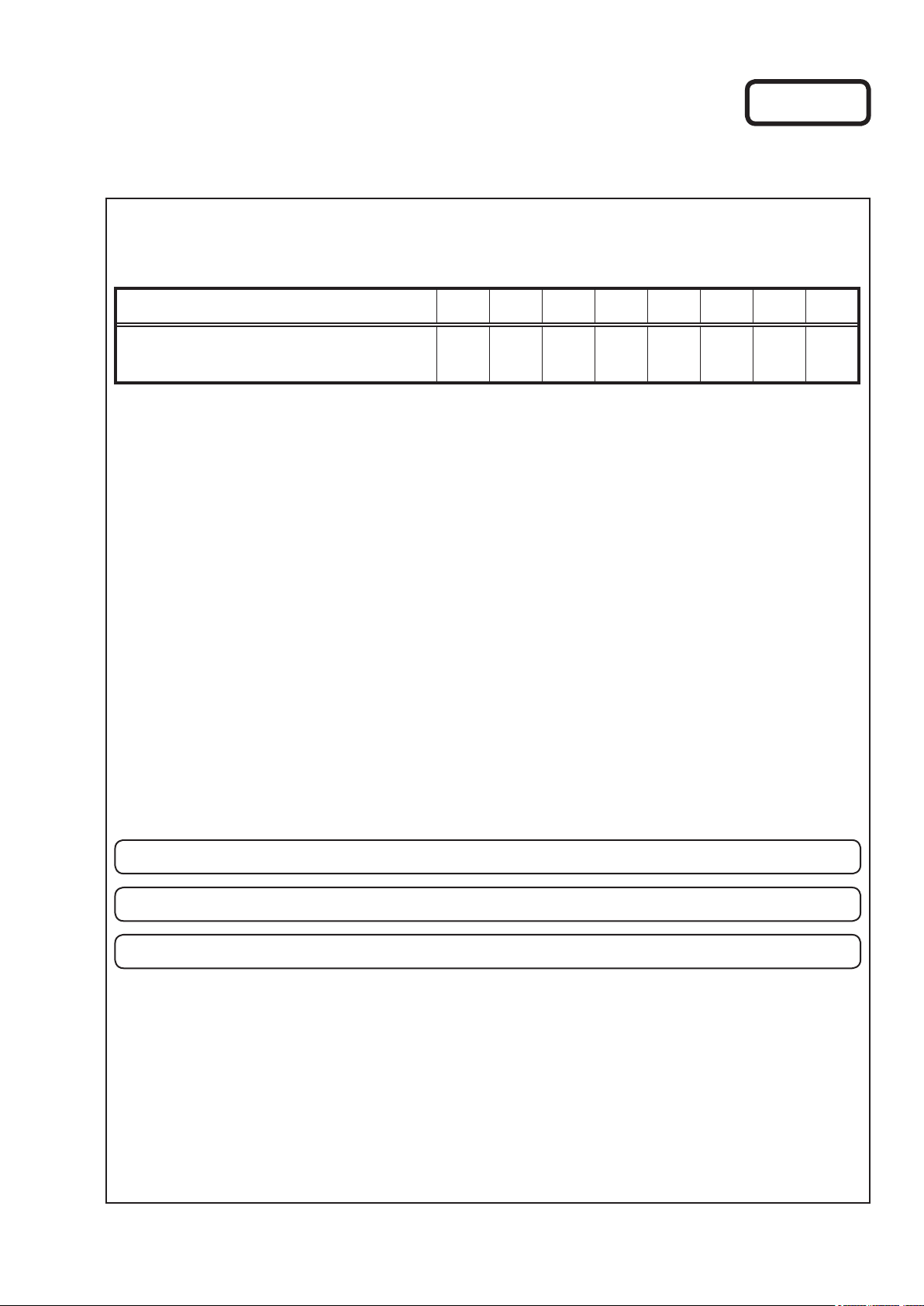
PWB Name Ref. No. Description
DIGITAL
DIGITAL
DIGITAL
IC91 STM32F101ZE
IC82 MX25L8006EM2I-12G
IC14 MX25L8006EM2I-12G
After
replaced
B
B
B
Remark
SOFTWARE: Main
SOFTWARE: DSP ROM
SOFTWARE: OSD ROM
After replacing
A
: Mask ROM (With software). No need for write-in of software to the microprocessor.
B
: Flash ROM (With software). Usually, no need for write-in of software. But, when the software was updated, you should
write the new software on the microprocessor or ash ROM. Please check the software version.
C
: Empty Flash ROM (Without software). You should write the software on the microprocessor or ash ROM.
Refer to "Update procedure" or "writing procedure", when you write the software.
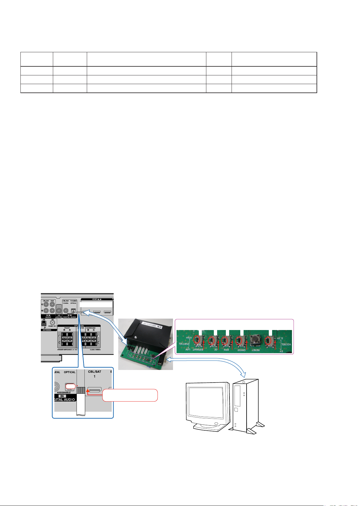
PROCEDURE FOR UPGRADING THE VERSION OF THE FIRMWARE
1. Preparations
1.1. Before starting the operation
(1) Personal Computer
(2) RS-232 cable (9P (Male), Straight).
(3) 8U-210100S WRITING KIT.
(4) 606050028012P / 7P FFC(1.0) L=240.
1.2. Connection of the AV receiver
(1) Conrm the power on/off switch of the AV receiver is turning off.
(2) Connect the update terminal of AV receiver with the "WRITING KIT".
(Refer to gure below for the connection of the 7P FFC cable.)
(3) Connect the RS-232C cable from PC with the "WRITING KIT".
7P FFC Cable
RS-232C Cable
WRITING KIT
1 pin
This side is contacts of
7P FFC Cable.
7P FFC Cable
S706-709 : HIGE
S709
S708
S707
S706
S702 : 3.3V
S702
PC
1.2. Connection of the AV receiver
(1) Conrm the power on/off switch of the AV receiver is turning off.
(2) Connect the update terminal of AV receiver with the "WRITING KIT".
(Refer to gure below for the connection of the 7P FFC cable.)
18

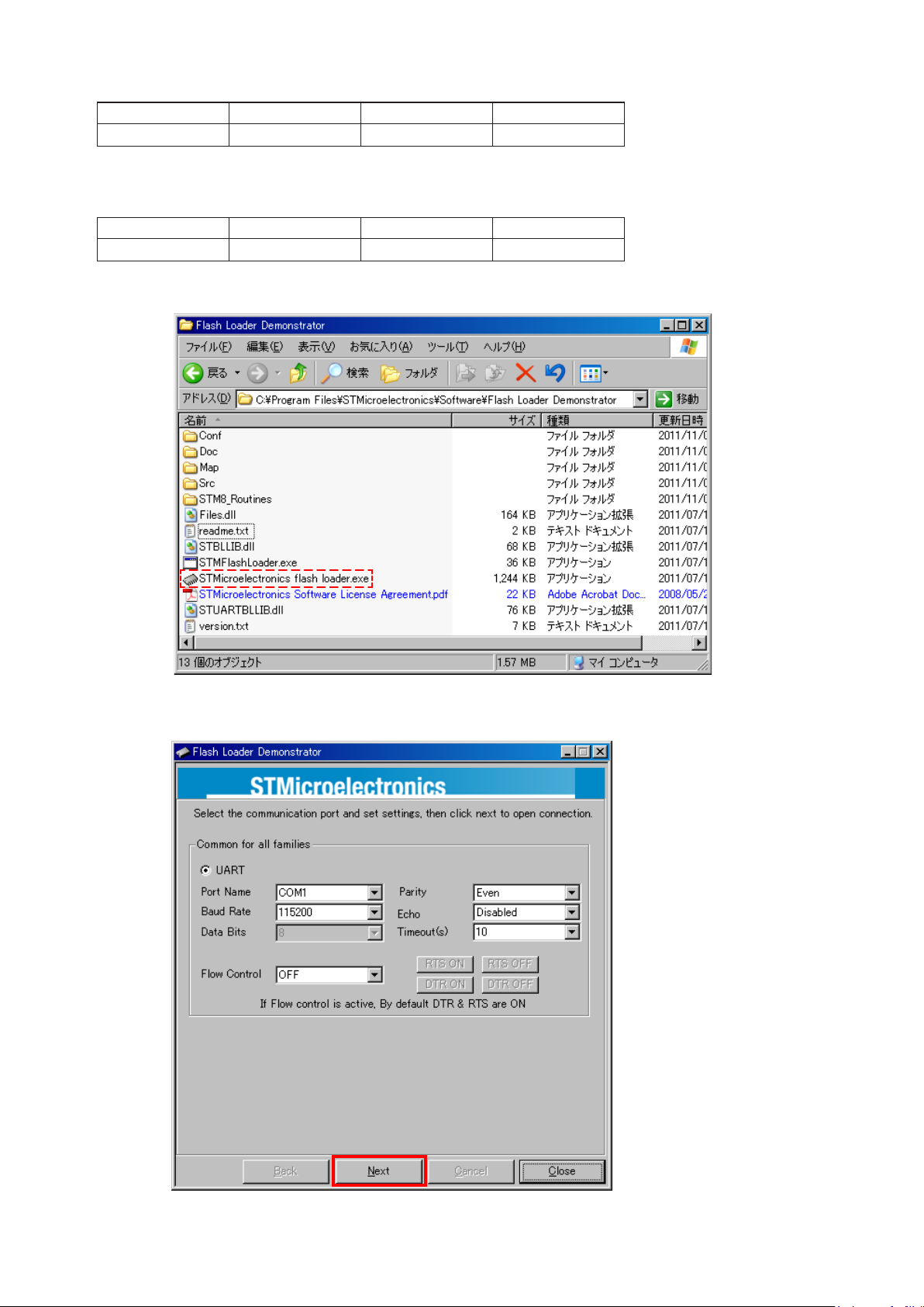
1.3. INSTALL UPDATE TOOL
(1) Click the "ST_Flash_Loder" folder.
(2) Run the "Flash_Loader_Demonstrator_v2.4.0_Setup.exe" on program le.
The following screen will be displayed.
The Setup Status bar appears.
19

(3) Click the "Next" button.
(4) Click the "Yes" button.
20
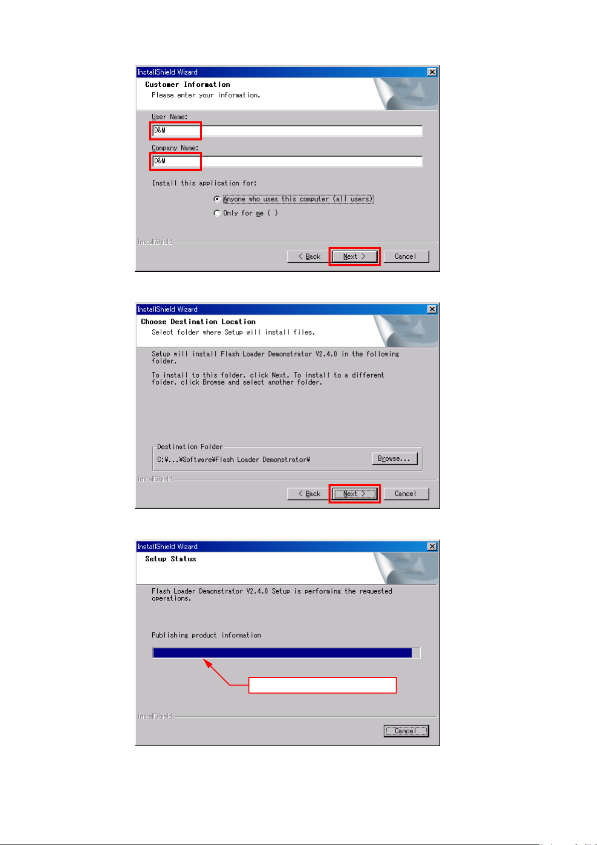
(5) Click the "Next" button after inputting "User Name" and "Company Name".
(6) Click the "Next" button.
The following screen will be displayed.
The Setup Status bar appears.
21
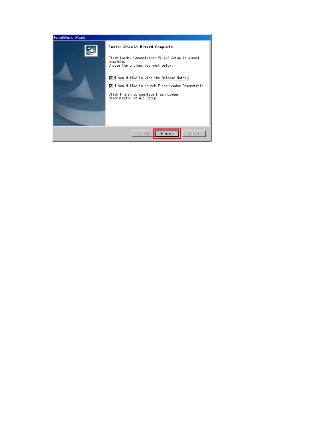
(7) Click the "Finish" button.
22
2. UPDATE FIRMWARE
(1) Connect the update terminal of AV receiver with the "WRITING KIT".
(2) Set the switch of "WRITING KIT". (Refer to the table below.)
DSPBOOT CE EPM CNVSS
H
H
(3) Press the X button to turn the power on of AV receiver.
(4) Set the switch of "WRITING KIT". (Refer to the table below.)
DSPBOOT CE EPM CNVSS
H
H
(5) Press the "RESET" switch of "WRITING KIT".
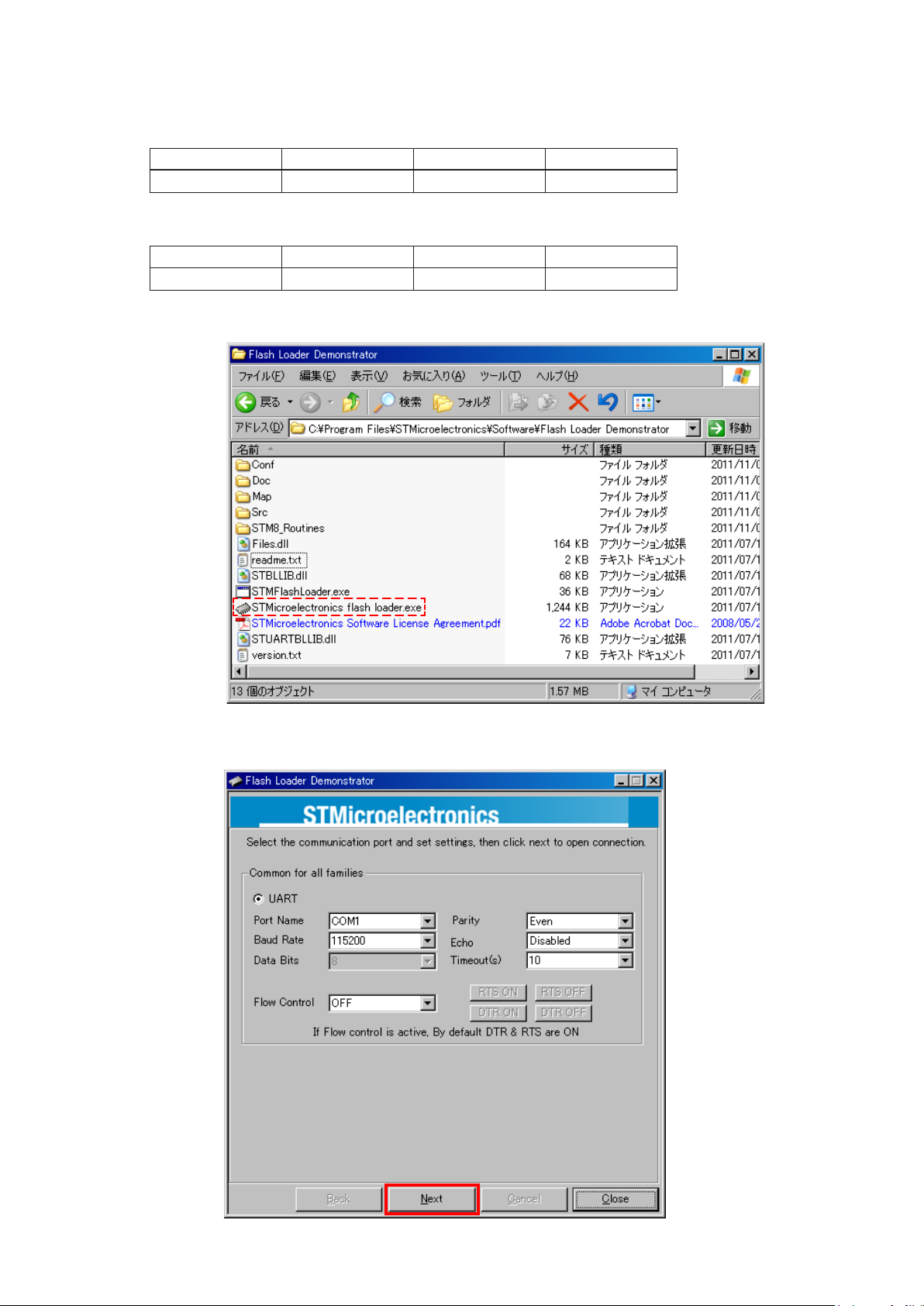
(6) Run the "STMicroelectronics ash loader.exe" on program le.
L
H
H
H
(7) Click the “Next” button 3 times.
Click the “Next” button for 1st time.
23

Click the “Next” button for 2nd time.
Click the “Next” button for 3rd time.
24
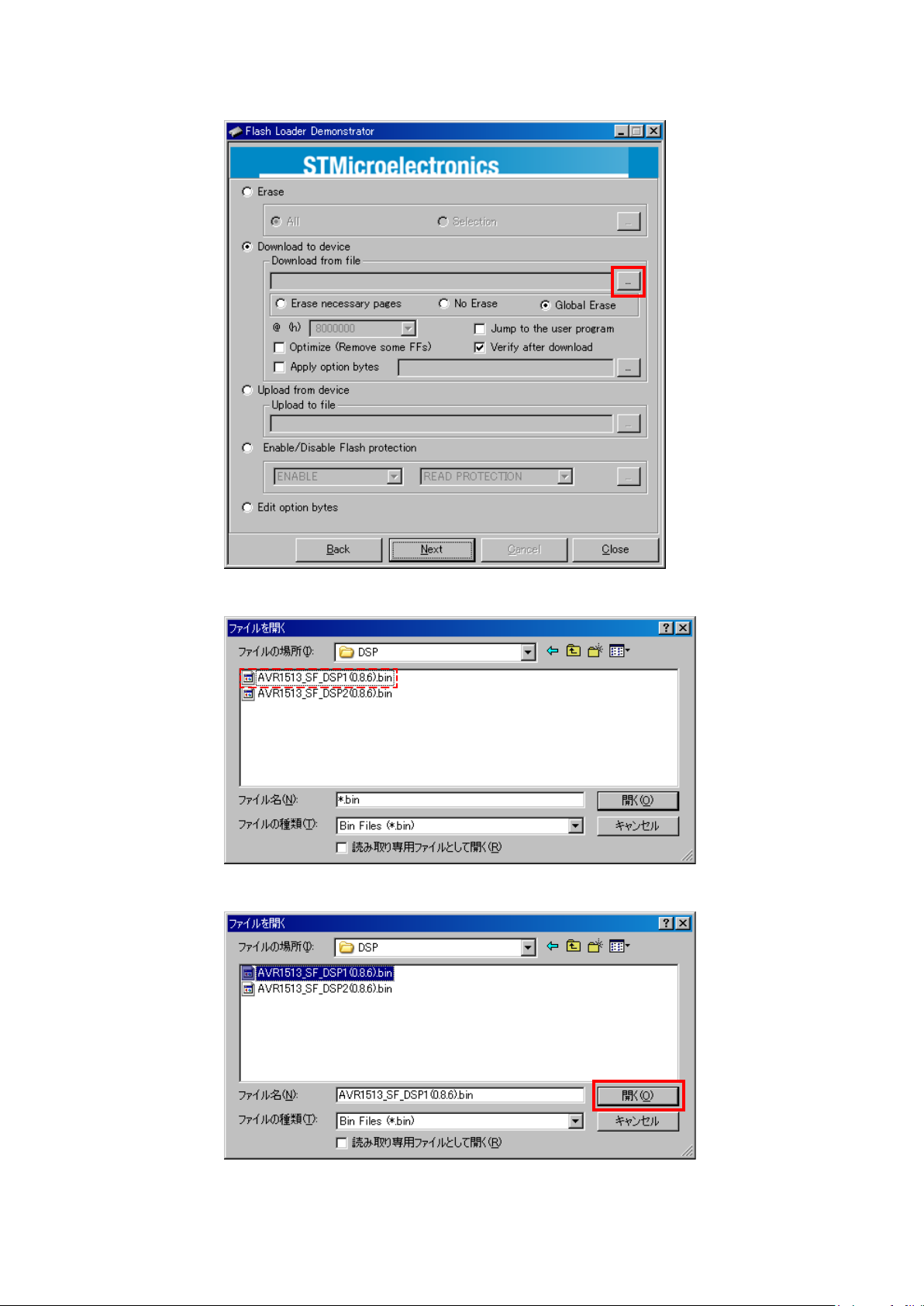
(8) Choose Flash File(DSP1).
Click the following button.
From the le browser windows select le of "AVR1513_SF_DSP1(x.x.x).bin".
Click the "Open" button.
25
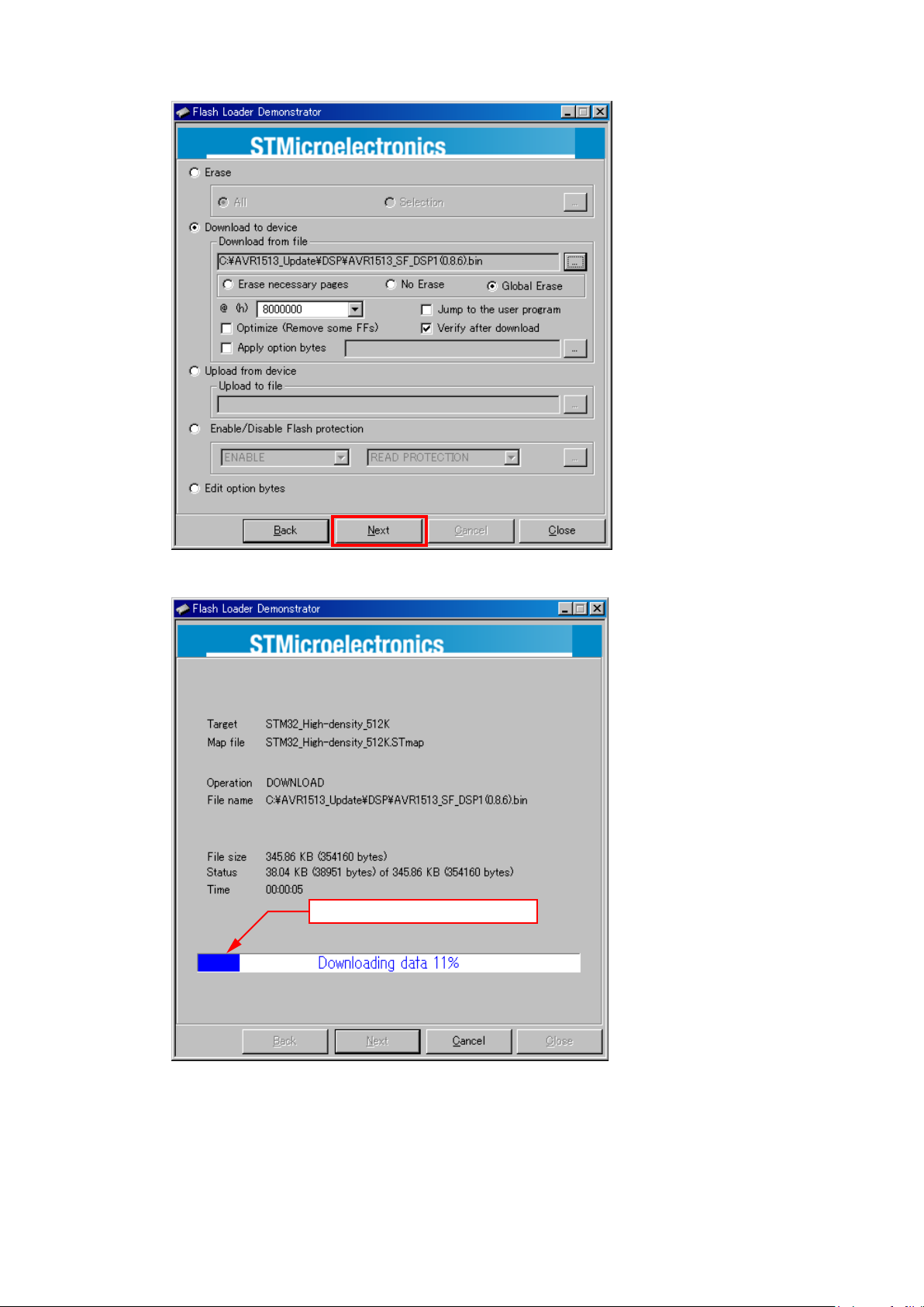
Click the “Next” button.
The following screen will be displayed.
The Setup Status bar appears.
26

The following screen will be displayed and click the "Close" button.
27
(9) Set the switch of "WRITING KIT". (Refer to the table below.)
DSPBOOT CE EPM CNVSS
H
H
L
(10) Press the "RESET" switch of "WRITING KIT".
Wait for about 130 seconds until "Write Complete." is displayed on VFD.
(11) Set the switch of "WRITING KIT". (Refer to the table below.)
DSPBOOT CE EPM CNVSS
H
H
H
(12) Press the "RESET" switch of "WRITING KIT".
(13) Re-run the "STMicroelectronics ash loader.exe" on program le.
H
H
(14) Click the “Next” button 3 times.
Click the “Next” button for 1st time.
28

Click the “Next” button for 2nd time.
Click the “Next” button for 3rd time.
29
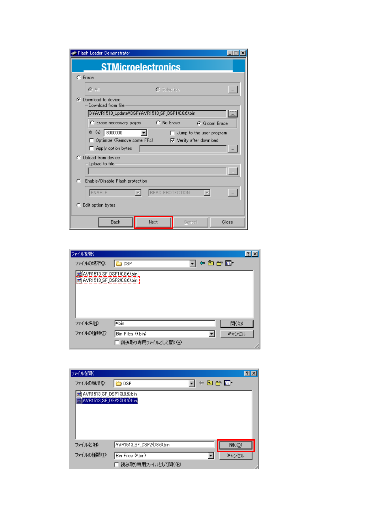
(15) Choose Flash File(DSP2).
Click the following button.
From the le browser windows select le of "AVR1513_SF_DSP2(x.x.x).bin".
Click the "Open" button.
30
 Loading...