

Page 1
Denon Brand Company, D&M Holdings lnc.
●
For purposes of improvement, specifications and
design are subject to change without notice.
●
Please use this service manual with referring to the
operating instructions without fail.
●
Some illustrations using in this service manual are
slightly different from the actual set.
注 意
サービスをおこなう前に、このサービスマニュアルを
必ずお読みください。本機は、火災、感電、けがなど
に対する安全性を確保するために、さまざまな配慮を
おこなっており、また法的には「電気用品安全法」に
もとづき、所定の許可を得て製造されております。
従ってサービスをおこなう際は、これらの安全性が維
持されるよう、このサービスマニュアルに記載されて
いる注意事項を必ずお守りください。
●
本機の仕様は性能改良のため、予告なく変更すること
があります。
●
補修用性能部品の保有期間は、製造打切後 8 年です。
●
修理の際は、必ず取扱説明書を参照の上、作業を行っ
てください。
●
本文中に使用しているイラストは、説明の都合上現物
と多少異なる場合があります。
Ver. 3
Please refer to the
MODIFICATION NOTICE.
SERVICE MANUAL
MODEL JP E3 E2 EK E2A E1C EA
AVR-1909
AVR-789
AVC-1909
33
33
3
AV SURROUND RECEIVER
X0383 V.03 DE/CDM 0812
Page 2
SAFETY PRECAUTIONS
The following check should be performed for the continued protection of the customer and service technician.
LEAKAGE CURRENT CHECK
Before returning the unit to the customer, make sure you make either (1) a leakage current check or (2) a line to chassis
resistance check. If the leakage current exceeds 0.5 milliamps, or if the resistance from chassis to either side of the
power cord is less than 460 kohms, the unit is defective.
CAUTION
Please heed the points listed below during servicing and inspection.
◎ Heed the cautions!
Spots requiring particular attention when servicing, such
as the cabinet, parts, chassis, etc., have cautions indicated
on labels or seals. Be sure to heed these cautions and the
cautions indicated in the handling instructions.
◎ Caution concerning electric shock!
(1) An AC voltage is impressed on this set, so touching in-
ternal metal parts when the set is energized could
cause electric shock. Take care to avoid electric shock,
by for example using an isolating transformer and
gloves when servicing while the set is energized, unplugging the power cord when replacing parts, etc.
(2)There are high voltage parts inside. Handle with extra
care when the set is energized.
◎ Caution concerning disassembly and
assembly!
Though great care is taken when manufacturing parts from
sheet metal, there may in some rare cases be burrs on the
edges of parts which could cause injury if fingers are
moved across them. Use gloves to protect your hands.
◎ Inspect for safety after servicing!
Check that all screws, parts and wires removed or disconnected for servicing have been put back in their original positions, inspect that no parts around the area that has been
serviced have been negatively affected, conduct an insulation check on the external metal connectors and between
the blades of the power plug, and otherwise check that
safety is ensured.
(Insulation check procedure)
Unplug the power cord from the power outlet, disconnect
the antenna, plugs, etc., and turn the power switch on. Using a 500V insulation resistance tester, check that the insulation resistance between the terminals of the power
plug and the externally exposed metal parts (antenna terminal, headphones terminal, microphone terminal, input
terminal, etc.) is 1MΩ or greater. If it is less, the set must
be inspected and repaired.
CAUTION
Concerning important safety
parts
◎ Only use designated parts!
The set's parts have specific safety properties (fire resistance, voltage resistance, etc.). For replacement parts, be
sure to use parts which have the same properties. In particular, for the important safety parts that are marked z on
wiring diagrams and parts lists, be sure to use the designated parts.
◎ Be sure to mount parts and arrange
the wires as they were originally!
For safety reasons, some parts use tape, tubes or other insulating materials, and some parts are mounted away from
the surface of printed circuit boards. Care is also taken with
the positions of the wires inside and clamps are used to
keep wires away from heating and high voltage parts, so
be sure to set everything back as it was originally.
Many of the electric and structural parts used in the set
have special safety properties. In most cases these properties are difficult to distinguish by sight, and using replacement parts with higher ratings (rated power and
withstand voltage) does not necessarily guarantee that
safety performance will be preserved. Parts with safety
properties are indicated as shown below on the wiring diagrams and parts lists is this service manual. Be sure to replace them with parts with the designated part number.
(1) Schematic diagrams ... Indicated by the z mark.
(2) Parts lists ... Indicated by the z mark.
Using parts other than the designated
parts could result in electric shock, fires or
other dangerous situations.
2
AVR-1909/789, AVC-1909
Page 3

注 意
サービス、点検時にはつぎのことにご注意願います。
◎注意事項をお守りください!
サービスのとき特に注意を必要とする個所については
キャビネット、部品、シャーシなどにラベルや捺印で注意
事項を表示しています。これらの注意書きおよび取扱説明
書などの注意事項を必ずお守りください。
◎感電に注意!
(1) このセットは、交流電圧が印加されていますので通電
時に内部金属部に触れると感電することがあります。
従って通電サービス時には、絶縁トランスの使用や手
袋の着用、部品交換には、電源プラグを抜くなどして
感電にご注意ください。
(2) 内部には高電圧の部分がありますので、通電時の取扱
には十分ご注意ください。
◎分解、組み立て作業時のご注意!
板金部品の端面の『バリ』は、部品製造時に充分管理をし
ておりますが、板金端面は鋭利となっている箇所が有りま
すので、部品端面に触れたまま指を動かすとまれに怪我を
する場合がありますので十分注意して作業して下さい。手
の保護のために手袋を着用してください。
◎指定部品の使用!
セットの部品は難燃性や耐電圧など安全上の特性を持っ
たものとなっています。従って交換部品は、使用されてい
たものと同じ特性の部品を使用してください。特に配線
図、部品表にz印で指定されている安全上重要な部品は
必ず指定のものをご使用ください。
◎部品の取付けや配線の引きまわしは、
元どおりに!
安全上、テープやチューブなどの絶縁材料を使用したり、
プリント基板から浮かして取付けた部品があります。また
内部配線は引きまわしやクランパーによって発熱部品や
高圧部品に接近しないように配慮されていますので、これ
らは必ず元どおりにしてください。
◎サービス後は安全点検を!
サービスのために取り外したねじ、部品、配線などが元ど
おりになっているか、またサービスした個所の周辺を劣化
させてしまったところがないかなどを点検し、外部金属端
子部と、電源プラグの刃の間の絶縁チェックをおこなうな
ど、安全性が確保されていることを確認してください。
(絶縁チェックの方法)
電源コンセントから電源プラグを抜き、アンテナやプラグ
などを外し、電源スイッチを入れます。500V 絶縁抵抗計
を用いて、電源プラグのそれぞれの端子と外部露出金属部
[アンテナ端子、ヘッドホン端子、マイク端子、入力端子
など]との間で、絶縁抵抗値が1 MΩ 以上であることを
確認してください。この値以下のときはセットの点検修理
が必要です。
注 意
本機に使用している多くの電気部品、および機構部品は安
全上、特別な特性を持っています。この特性はほとんどの
場合、外観では判別つきにくく、またもとの部品より高い
定格(定格電力、耐圧)を持ったものを使用しても安全性
が維持されるとは、限りません。安全上の特性を持った部
品は、このサービスマニュアルの配線図、部品表につぎの
ように表示していますので必ず指定されている部品番号
のものを使用願います。
(1) 配線図…zマークで表示しています。
(2) 部品表…zマークで表示しています。
安全上重要な部品について
指定された部品と異なるものを使用した場
合には、感電、火災などの危険を生じる恐
れがあります。
3
AVR-1909/789, AVC-1909
Page 4
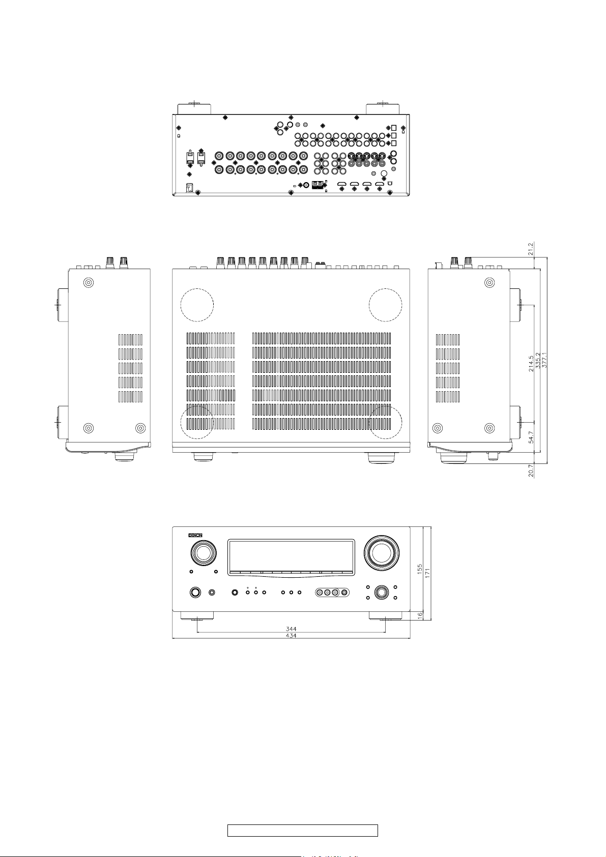
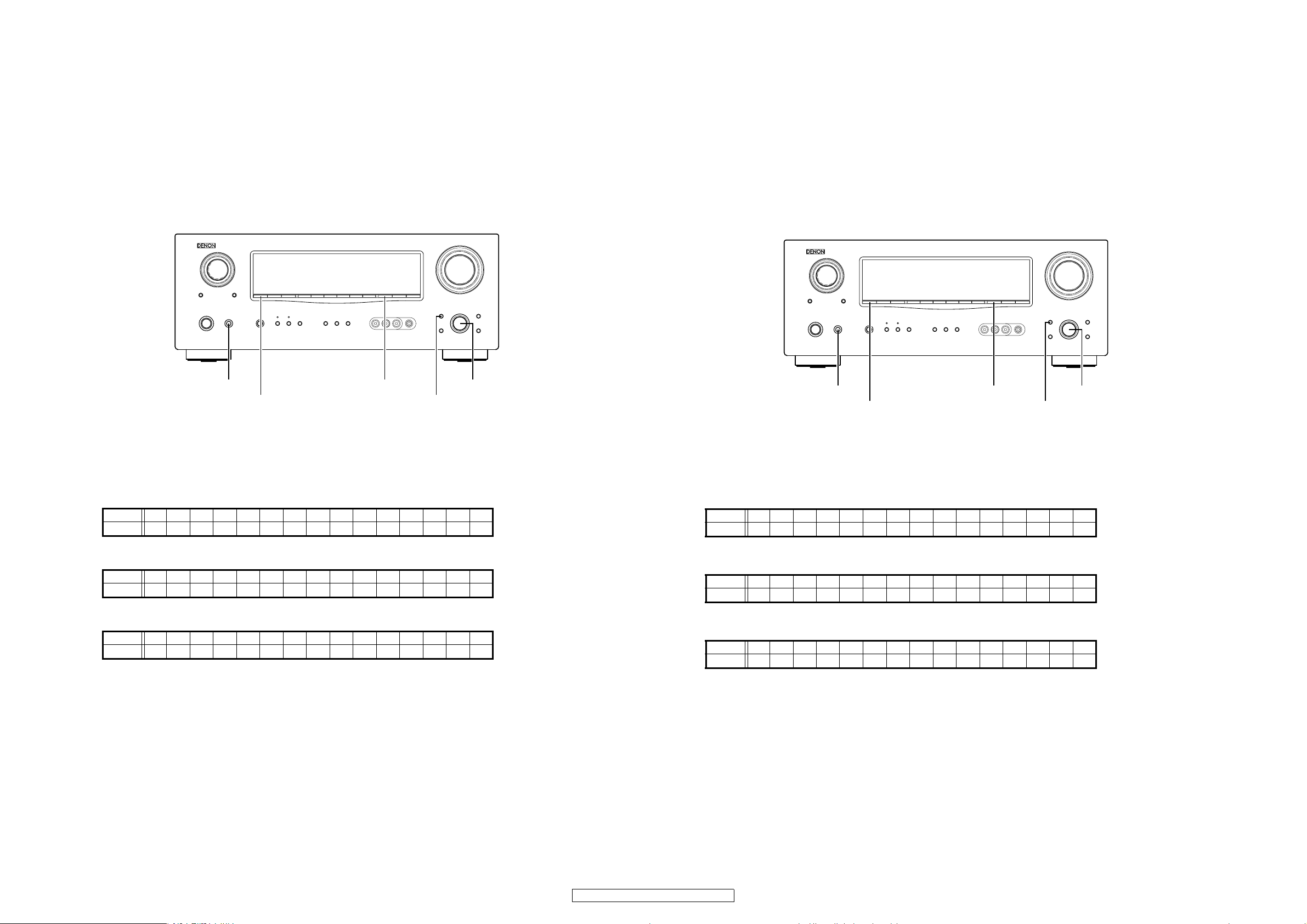
DIMENSION
AVR-1909 model
4
AVR-1909/789, AVC-1909
Page 5
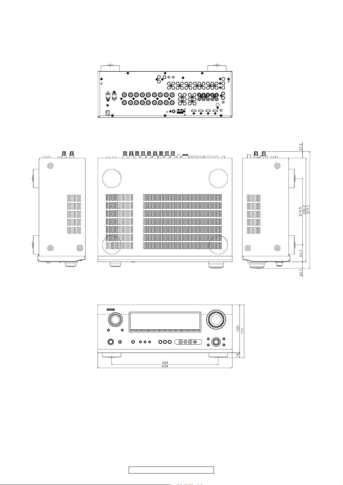
AVR-789 model
5
AVR-1909/789, AVC-1909
Page 6

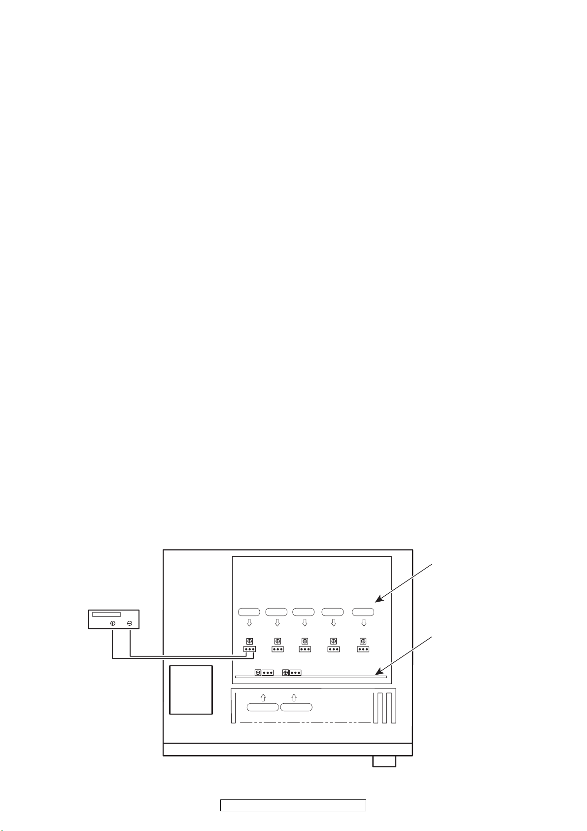
WIRE ARRANGEMENT
If wire bundles are untied or moved to perform adjustment or
parts replacement etc., be sure to rearrange them neatly as
they were originally bundled or placed afterward.
Otherwise, incorrect arrangement can be a cause of noise
generation.
ワイヤー整形図
調整や部品の交換等により、ワイヤー類の結束をはずした
り移動させた場合には、それらの作業が完了した時点でワ
イヤーの整形をおこなってください。正しく整形されてい
ないとノイズ発生の原因となることがあります。
Wire arrangement viewed from the top
上面からみたワイヤー整形
Back Panel side
Front Panel side
6
AVR-1909/789, AVC-1909
Page 7
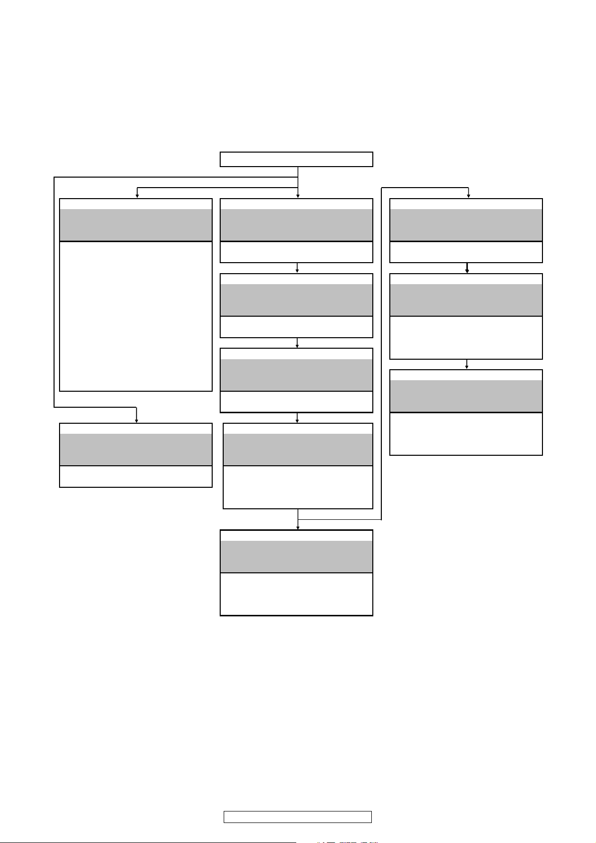
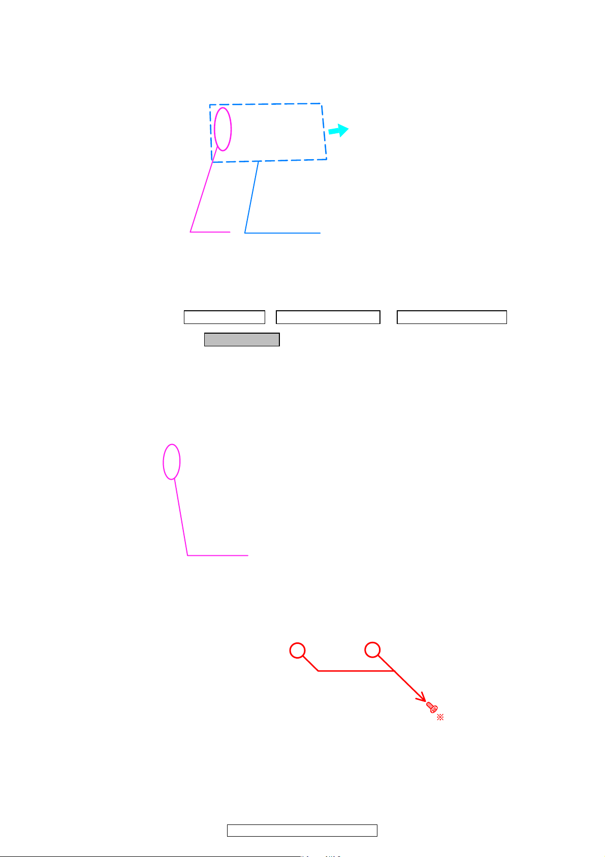
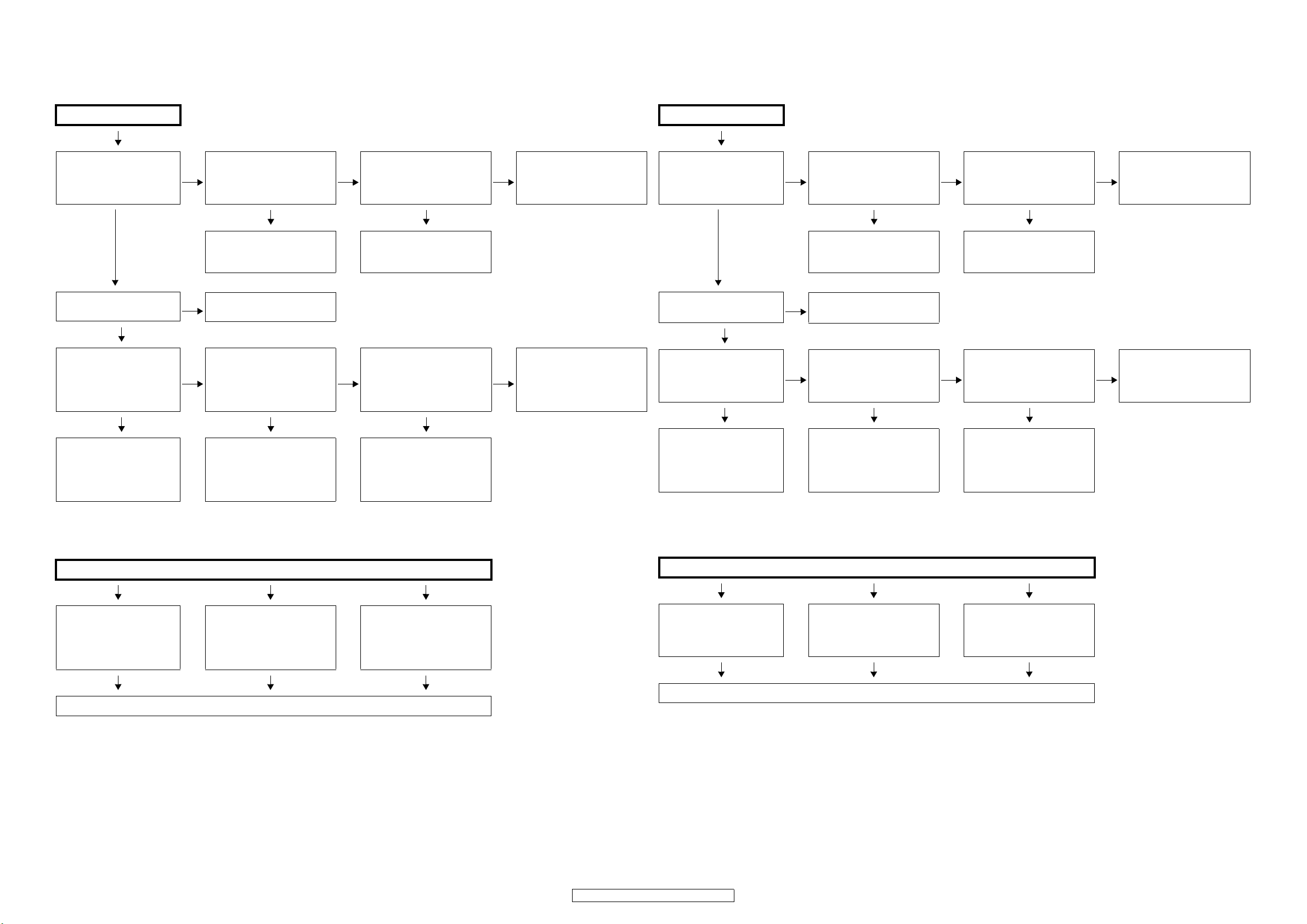
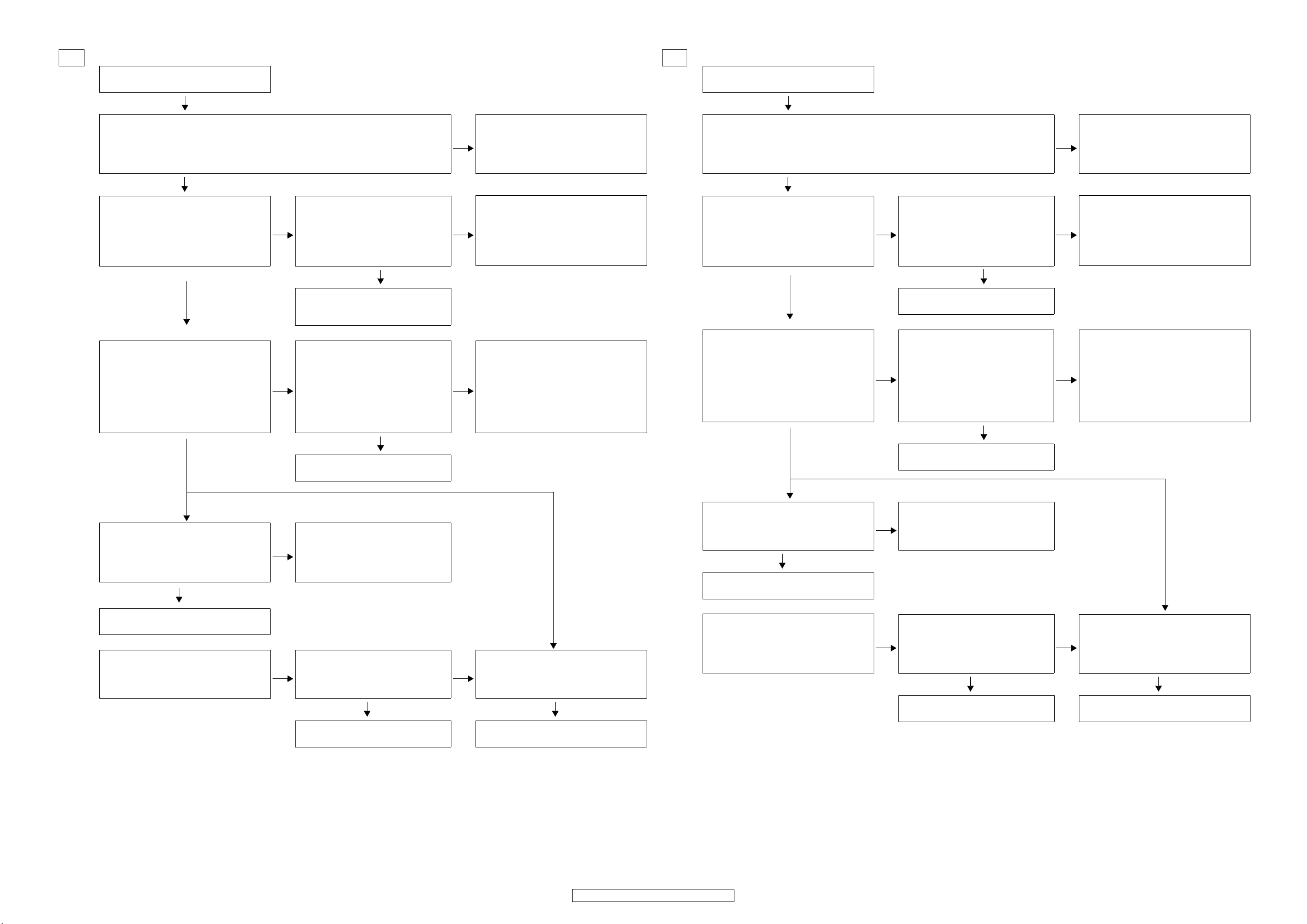
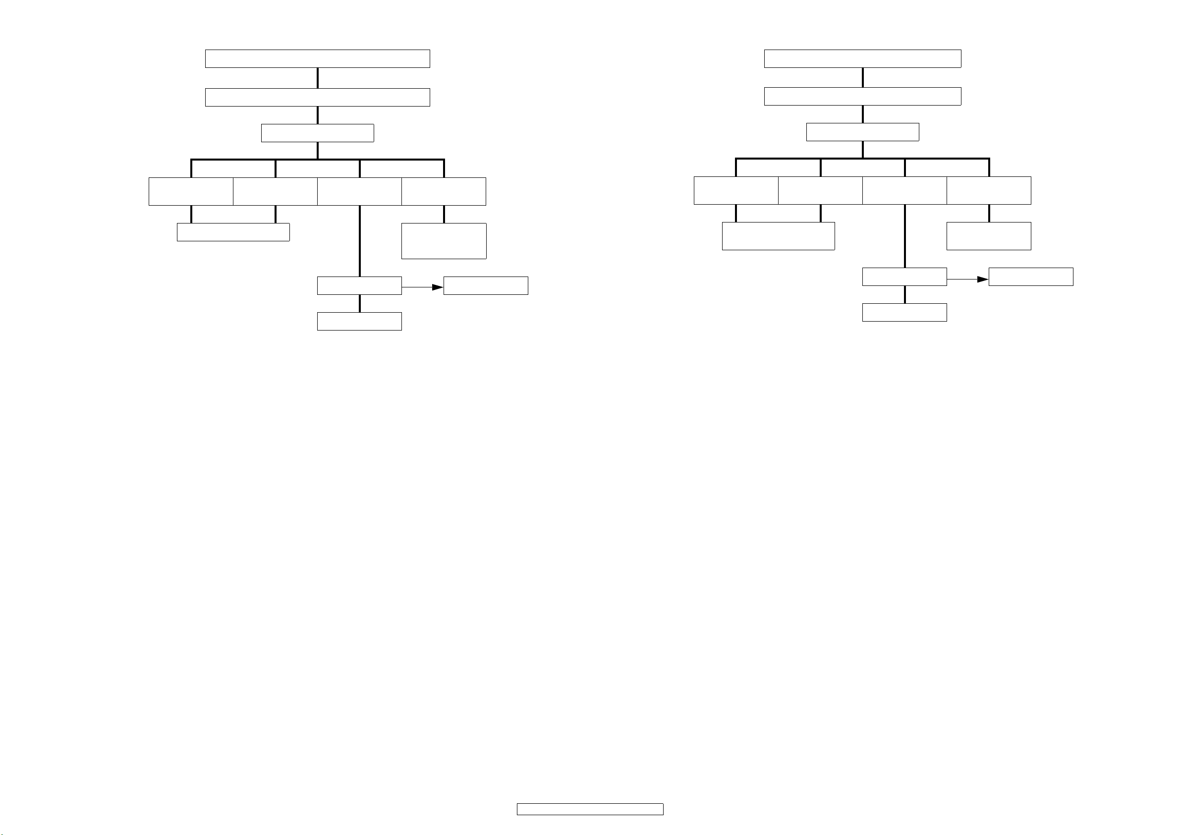
DISASSEMBLY
K
• Disassemble in order of the arrow of the figure of following flow.
下記フロー図の矢印の順番にはずしてください。
• In the case of the re-assembling, assemble it in order of the reverse of the following flow.
再組み立ての場合は、下記のフローの逆の順番に組立ててください
• In the case of the re-assembling, observe "attention of assembling" it.
再組み立ての場合は、「組立のご注意」を遵守してください。
CABINET TOP
㩷
PANEL FRONT SUB ASSY
Refer to "DISASSEMBLY
1.PANEL FRONT SUB ASSY"
and "EXPLODED VIEW"
FRONT P.W.B ASSY HDMI P.W.B ASSY VIDEO P.W.B ASSY
(Ref. No. of EXPLODED VIEW : BF1) (Ref. No. of EXPLODED VIEW : BH1) (Ref. No. of EXPLODED VIEW : BV1)
V- AUX P.W.B ASSY
(Ref. No. of EXPLODED VIEW : BF2)
MIC P.W.B ASSY
(Ref. No. of EXPLODED VIEW : BF3)
FUNC P.W.B ASSY
(Ref. No. of EXPLODED VIEW : BF4) SIRIUS P.W.B ASSY CPU P.W.B ASSY
HEAD PHONE P.W.B ASSY (Ref. No. of EXPLODED VIEW : BS1) (Ref. No. of EXPLODED VIEW : BC1)
(Ref. No. of EXPLODED VIEW : BF6) INPUT P.W.B ASSY
POWER SW P.W.B ASSY (Ref. No. of EXPLODED VIEW : BI1)
(Ref. No. of EXPLODED VIEW : BF7)
ENCORDER P.W.B ASSY
(Ref. No. of EXPLODED VIEW : BF8)
TUNER PACK
(Ref. No. of EXPLODED VIEW : PR1)
TRANS CHASSIS BACK SUB ASSY
Refer to "DISASSEMBLY
10.TRANS"
and "EXPLODED VIEW"
TRANS CHASSIS BACK SUB ASSY
(Ref. No. of EXPLODED VIEW : W8) (Ref. No. of EXPLODED VIEW : C2)
SPEAKER P.W.B ASSY
(Ref. No. of EXPLODED VIEW : BF5)
HDMI P.W.B ASSY
Refer to "DISASSEMBLY
2.HDMI P.W.B ASSY"
and "EXPLODED VIEW"
SIRIUS P.W.B ASSY
Refer to "DISASSEMBLY
3.SIRIUS P.W.B ASSY"
and "EXPLODED VIEW"
TUNER PAC
Refer to "DISASSEMBLY
4.TUNER PACK"
and "EXPLODED VIEW"
Refer to "DISASSEMBLY
5.CHASSIS BACK SUBASSY"
and "EXPLODED VIEW"
MAIN P.W.B ASSY
(Ref. No. of EXPLODED VIEW : BM1)
2CH P.W.B ASSY
(Ref. No. of EXPLODED VIEW : B21)
VIDEO P.W.B ASSY
Refer to "DISASSEMBLY
6.VIDEO P.W.B ASSY"
and "EXPLODED VIEW"
INPUT / CPU P.W.B ASSY
Refer to "DISASSEMBLY
7.INPUT / CPU P.W.B ASSY"
and "EXPLODED VIEW"
MAIN P.W.B SUB ASSY
Refer to "DISASSEMBLY
8.MAIN P.W.B SUB ASSY"
and "EXPLODED VIEW"
POWER P.W.B SUB ASSY
Refer to "DISASSEMBLY
9.POWER P.W.B SUB ASSY"
and "EXPLODED VIEW"
POWER P.W.B ASSY
(Ref. No. of EXPLODED VIEW : BP1)
POWER SUPPLY P.W.B ASSY
(Ref. No. of EXPLODED VIEW : BP2)
7
AVR-1909/789, AVC-1909
Page 8
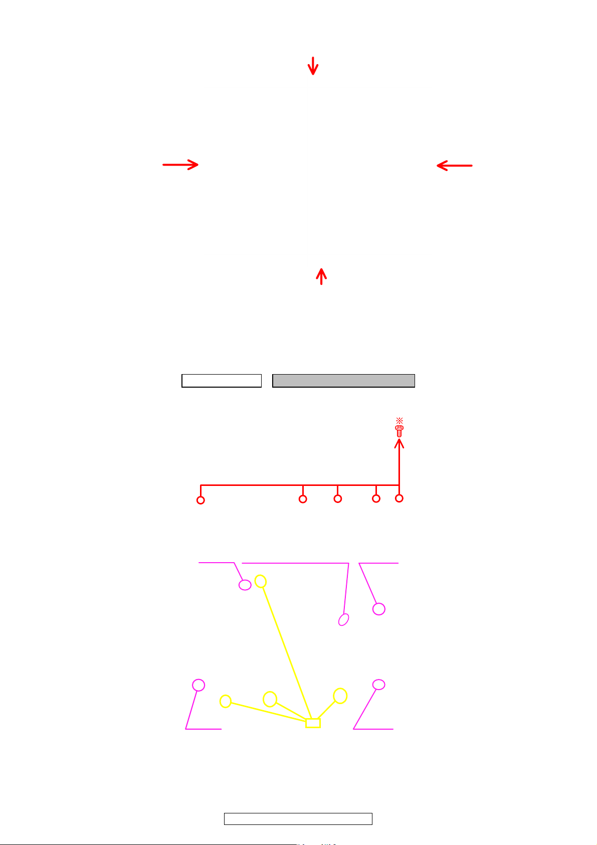
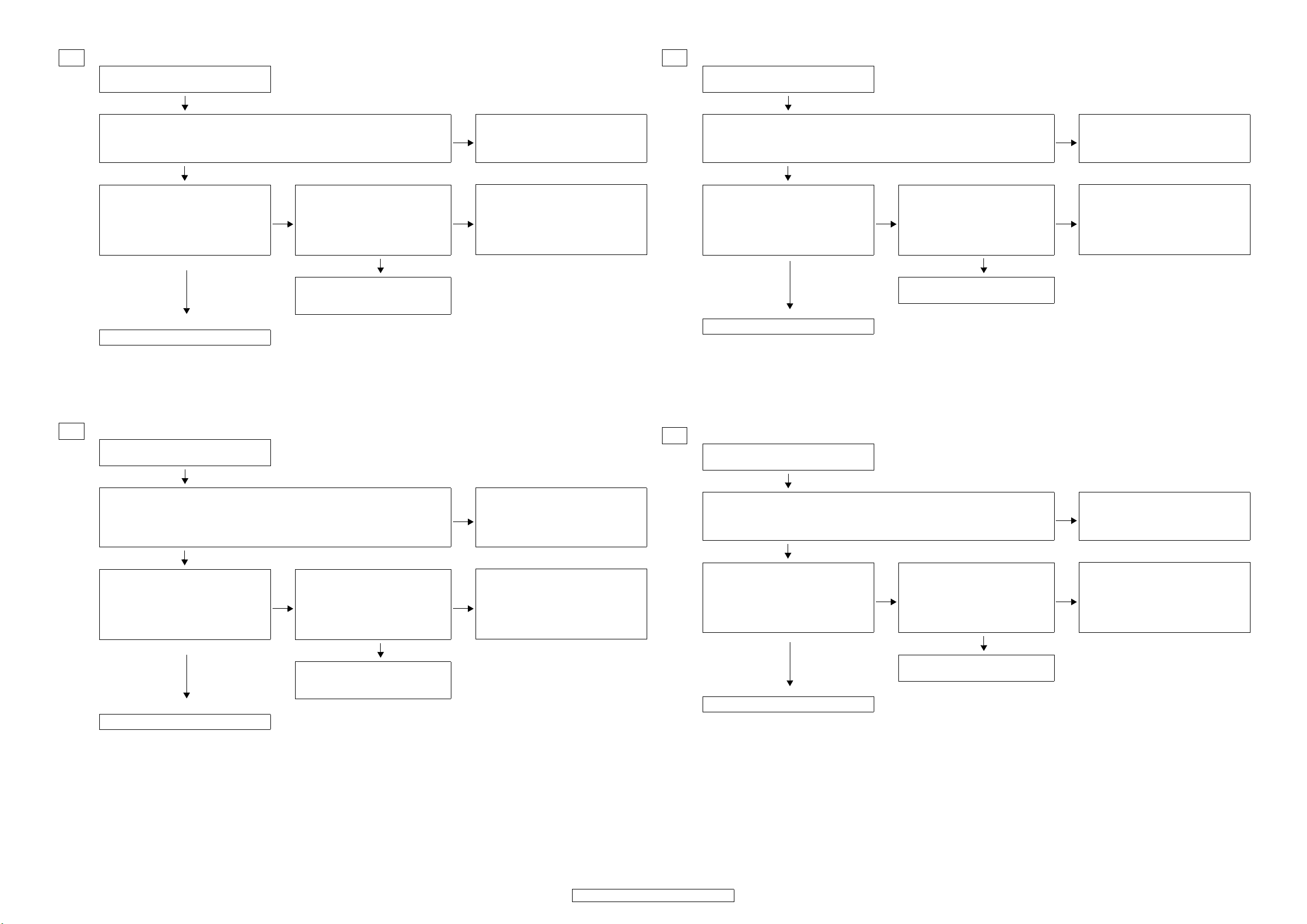
The viewpoint of each photograph
(photography direction)
Front side
各図の視点(撮影方向)
Top view
Picture A
Picture C
Picture B
1. PANEL FRONT SUB ASSY
proceeding (手順): CABINET TOP → PANEL FRONT SUB ASSY
(1) Remove the screws.(ねじをはずす。)
Picture D
Bottom view
(2) Disconnect the connector wires.(コネクタワイヤーをはずす。)
CP541
Top view
CP503
CORD HOLDER : Loose
cut
CP302
CN301
8
AVR-1909/789, AVC-1909
Page 9
(3) Disconnect the FFC cable.(FFC ケーブルをはずす。)
Picture C
CORD HOLDER : Loose
(4) Remove the screw.(ねじをはずす。)
Top view
FFC CABLE
(5) Disconnect the connector wire.(コネクタワイヤーをはずす。)
Picture C
CN306
Please refer to "EXPLODED VIEW " for the disassembly method of each P.W.B included in PANEL FRONT SUB ASSY .
PANELFRONTSUBASSY の各基板のはずしかたは "EXPLODEDVIEW" を参照してください。
9
AVR-1909/789, AVC-1909
Page 10
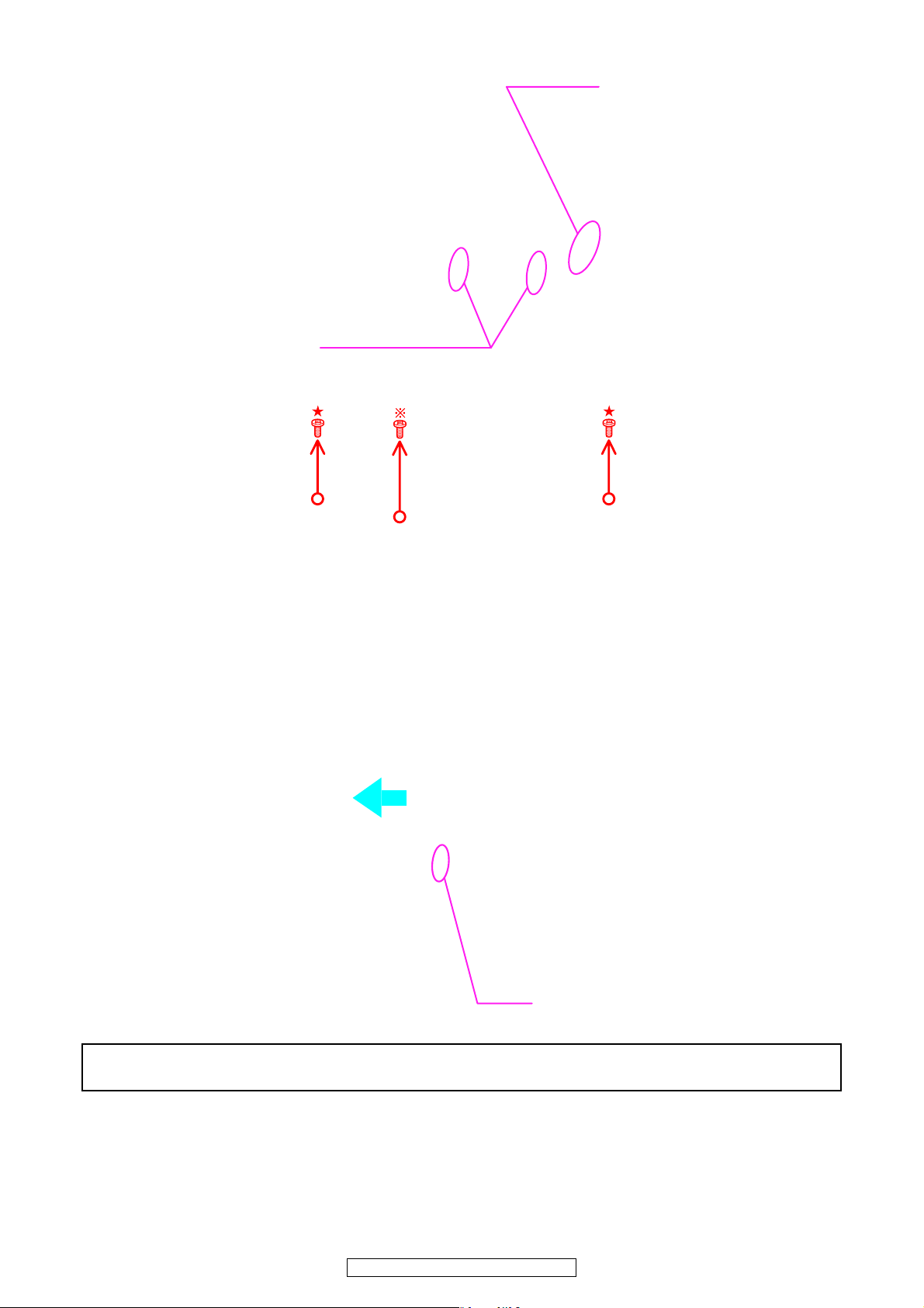
2. HDMI P.W.B.ASSY
proceeding (手順): CABINET TOP → HDMI P.W.B ASSY
(1) Remove the screws.(ねじをはずす。)
Picture B
(2) Disconnect the connector wires and boards.(コネクタワイヤーとコネクタボードをはずす。)
Picture B
HDMI P.W.B ASSY
Board to board
CP1007 CP1005
3. SIRIUS P.W.B ASSY
proceeding (手順): CABINET TOP → HDMI P.W.B ASSY → SIRIUS P.W.B ASSY
(1) Remove the screw.(ねじをはずす。)
Picture B
10
AVR-1909/789, AVC-1909
Page 11
(2) Disconnect the connector wire.(コネクタワイヤーをはずす。)
Top view
CP901
SIRIUS ASSY
4. TUNER PACK
proceeding (手順): CABINET TOP → HDMI P.W.B ASSY → SIRIUS P.W.B ASSY
→ TUNER PACK
(1) Disconnect the FFC cable.(FFCケーブルをはずす。)
To p vi ew
FFC CABLE
(2) Remove the screws.(ねじをはずす。)
Picture B
11
AVR-1909/789, AVC-1909
Page 12
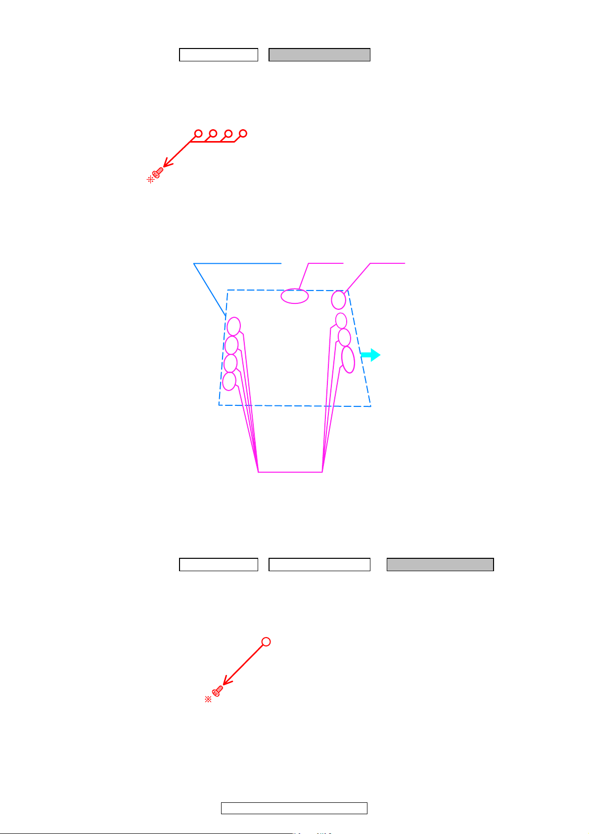
5. CHASSIS BACK SUB ASSY
proceeding (手順): CABINET TOP → HDMI P.W.B ASSY → SIRIUS P.W.B ASSY
→ TUNER PACK → CHASSIS BACK SUB ASSY
(1) Disconnect the connector wires. (コネクタワイヤーをはずす。)
CP102B CP103
Top view
CP103 CP101
(2) Remove the screws.(ねじをはずす。)
cut
SPEAKER P.W.B ASSY
Picture B
ً
Picture B
SPEAKER P.W.B. ASSY
Please refer to "EXPLODED VIEW " for the disassembly method of each P.W.B included in CHASSIS BACK SUB ASSY .
CHASSISBACKSUBASSY の各基板のはずしかたは "EXPLODEDVIEW" を参照してください。
12
AVR-1909/789, AVC-1909
Page 13
6. VIDEO P.W.B ASSY
proceeding (手順): CABINET TOP → HDMI P.W.B ASSY → SIRIUS P.W.B ASSY
→ TUNER PACK → CHASSIS BACK SUB ASSY
→ VIDEO P.W.B ASSY
(1) Disconnect the connector wires and boards.(コネクタワイヤーとコネクタボードをはずす。)
Picture D
VIDEO P.W.B ASSY
Board to board
CP2010
SUPPORTER
CP2009CP2008Board to board
7. INPUT / CPU P.W.B ASSY
proceeding (手順): CABINET TOP → HDMI P.W.B ASSY → SIRIUS P.W.B ASSY
→ TUNER PACK → CHASSIS BACK SUB ASSY
→ VIDEO P.W.B ASSY → INPUT / CPU P.W.B ASSY
(1) Disconnect the FFC cable.(FFC ケーブルをはずす。)
CPU P.W.B ASSY
Picture C
FFC CABLE
13
AVR-1909/789, AVC-1909
Page 14
(2) Disconnect the connector wires and boards.(コネクタワイヤーとコネクタボードをはずす。)
INPUT P.W.B ASSY
Picture D
CP514
Picture D
CPU P.W.B ASSY
INPUT P.W.B ASSY
Board to board
Board to board
14
AVR-1909/789, AVC-1909
Page 15
8. MAIN P.W.B SUB ASSY
proceeding (手順): CABINET TOP → HDMI P.W.B ASSY → SIRIUS P.W.B ASSY
→ TUNER PACK → CHASSIS BACK SUB ASSY
→ VIDEO P.W.B ASSY → INPUT / CPU P.W.B ASSY
→ MAIN P.W.B SUB ASSY
Please refer to "EXPLODED VIEW " for the disassembly method of each P.W.B included in MAIN P.W.B ASSY .
MAINP.W.BASSY の各基板のはずしかたは "EXPLODEDVIEW" を参照してください。
9. POWER P.W.B SUB ASSY
proceeding (手順): CABINET TOP → HDMI P.W.B ASSY → SIRIUS P.W.B ASSY
→ TUNER PACK → CHASSIS BACK SUB ASSY
→ POWER P.W.B SUB ASSY
(1) Disconnect the connector wires and boards.(コネクタワイヤーとコネクタボードをはずす。)
cut cut
CP513 CP512
Picture C
Please refer to "EXPLODED VIEW " for the disassembly method of each P.W.B included in POWER P.W.B SUB ASSY.
POWERP.W.BSUBASSY の各基板のはずしかたは "EXPLODEDVIEW" を参照してください。
CP504
Board to board
CP503CP501
POWER P.W.B ASSY
POWER SUPPLY P.W.B ASSY
15
AVR-1909/789, AVC-1909
Page 16
10. TRANS
proceeding (手順): CABINET TOP → TRANS
(1) Disconnect the connector wires.(コネクタワイヤーをはずす。)
cut cut
To p vi ew
CP104 CN305
CP2008
CP302
cut cut
Picture C
Please refer to "EXPLODED VIEW " for the disassembly method of POWER TRANS.
POWERTRANS のはずしかたは "EXPLODEDVIEW" を参照してください。
CP513 CP512 CP501
16
AVR-1909/789, AVC-1909
Page 17
CAUTION IN SERVICING
サービス時の注意事項
Initializing AV SURROUND RECEIVER/AMPLIFIER
AV SURROUND RECEIVER/AMPLIFIER initialization should
be performed when the µcom, peripheral parts of µcom, and
Digital P.W.B. are replaced.
1. Switch off the unit.
2. With the "INPUTMODE" and "SPEAKERS" buttons
pressed, press the "ON/OFF" button to turn the power on.
3. Check that the entire display is flashing with an interval of
about 1 second, and release your fingers from the 2 buttons and the microprocessor will be initialized.
Note:・If step 3 does not work, start over from step 1.
・ All user settings will be lost and this factory setting
will be recovered when this initialization mode.
So make sure to m+emorize your setting for restoring after the initialization.
AVサラウンドレシーバー / アンプの初期化
について
マイコンやマイコン周辺部品、Digital 基板等を交換した場
合は、AV サラウンドレシーバー / アンプの初期化を行って
下さい。
1. "ON/OFF" ボタンを OFF にします。
2. "INPUTMODE" と "SPEAKERS" の 2 つのボタンを押した
状態で、"ON/OFF" ボタンを押して ON にします。
3. ディスプレイ表示が約 1秒間隔で点滅するのを確認後、
2つのボタンから指を離します。
*マイコンが初期化されます。
注意 :・上記 3 の状態にならない場合は、もう一度操作 1
からやり直してください。
・初期化を行うとお客様が設定した内容が工場出
荷状態に戻りますので、あらかじめ設定内容を
控えておき初期化後再設定してください。
ON/OFF SPEAKERS
INPUTMODE
JIG to use for servicing
When you repair the printing board, you can use the following
JIG (Extension cable kit). Please order to Denon Official Service Distributor in your region if necessary.
00D SPK- 561 EXTENSION UNIT KIT : 1 Set
00D SPK- 562 9120 CONN. JOINT KIT : 1 Set
When you update the firmware, you can use the following
JIG (RS232C to internal connector conversion adapter with
8P cable kit ). Please order to Denon Official Service Distributor in your region if necessary.
00DSPK-581 WRITING UNIT : 1 Set
サービス時に使用する治具について
基板を修理する際、使用する治具 ( 延長ケーブルキット)
は 下記のとおりです。
必要に応じて販社サービスへ注文下さい。
00DSPK-561EXTENSIONUNITKIT :1 式
00DSPK-5629120CONN.JOINTKIT :1 式
ファームウェアをアップデートする際、使用する治具
(RS232C →製品内部コネクタ変換基板 +8Pケーブルキッ
ト ) は下記のとおりです。
必要に応じて販社サービスへ注文ください。
00DSPK-581WRITINGUNIT :1 式
17
AVR-1909/789, AVC-1909
Page 18
Check mode for µcom/DSP version
STATUS
ON/OFF
RDS
DYN VOL
E2 model
マイコン・DSP バージョンのチェック方法
µcom/DSP Version Display Mode
1. Operation specifications
µcom/DSP version display mode:
When started up, the version information is displayed.
Starting up:
● E3, EA, JP model
With the "DYN VOL" and "VIDEO SELECT" buttons
pressed, press the "ON/OFF" button to turn the power on.
Now, press the "STATUS" button to the display the 2nd
item information on the FL Display.
● E2 model
With the "DYN VOL" and "RDS" buttons pressed, press
the "ON/OFF" button to turn the power on.
Now, press the "STATUS" button to the display the 2nd
item information on the FL Display.
E3, EA, JP model
マイコン・DSP バージョン表示モード
1. 動作仕様
マイコン、DSP バージョン表示モード :
起動状態にて、バージョン情報を表示します。
起動方法 :
● E3,EA,JP モデル
"DYNVOL" と "VIDEOSELECT" の 2 つのボタンを押した
状態で、"ON/OFF" ボタンを押して電源を入れます。
その後、"STATUS" ボタンを押すと 2 項の内容が FL
Display に表示されます。
● E2 モデル
"DYNVOL" と "RDS" の 2 つのボタンを押した状態で、
"ON/OFF" ボタンを押して電源を入れます。
その後、"STATUS"ボタンを押すと 2 項の内容が FLDisplay
に表示されます。
ON/OFF
STATUS
DYN VOL
VIDEO SELECT
2. Display Order
Destination information→Main-µcom version information
→ DSP version information
2. 表示順序
仕向地表示→メインマイコンバージョン情報→DSP
バージョン情報
18
AVR-1909/789, AVC-1909
Page 19
PROCEDURE FOR CHECKING ERRORS
ON/OFF MULTEQ ENTER
MENU
STATUS
ERROR 確認方法
Displaying the protection history
1. Operation specifications
ERROR MODE(displaying the protection history)
When started up, the error information is displayed.
Starting up:
With the "MENU" and "MULTEQ" buttons pressed, press the "ON/OFF" button to turn the power on. The error (protection history display) mode is set.
Now, press the "STATUS" button to turn on the FL display.
PROTECTION 履歴表示
1. 動作仕様
ERROR(PROTECTION 履歴表示 ) モード :
起動状態にて、ERROR 情報を表示します。
起動方法 :
"MENU" とMULTEQの2つのボタンを押した状態で、"ON/OFF" ボタンを押して電源を入れると、ERROR(PROTECTION 履歴表
示)モードとなります。
その後、STATUSボタンを押すと FLDisplay 表示されます。
ON/OFF MULTEQ ENTER
STATUS
2. About the display on the FL display
When the "STATUS" button is pressed after setting the error (protection history display) mode, a history like the one shown below is
displayed, depending on the conditions.
(1) Normally (when there has been no protection incident)
Upper P R O T E C T
Lower : N O P R O T E C T
(2) For ASO/DC (when the last protection incident was ASO or DC protection)
Upper P R O T E C T
Lower : A S O / D C
(3) For THERMAL (when the last protection incident was THERMALprotection)
Upper P R O T E C T
Lower : T H E R M A L
When the "STATUS" button is pressed again after the above protection history is displayed, the normal display reappears.
ISTORY
H
ISTORY
H
ISTORY
H
MENU
2. FLDisplay 表示に関して
ERROR(PROTECTION 履歴表示)モード後に、STATUSボタンを押すと、状況によって以下ような履歴を表示します。
(1) 正常時 ( 今まで PROTECTION が発生していない場合 )
上段
下段
(2) ASO/DC 時 ( 最後の PROTECTION が ASO または DCPROTECTION の場合 )
上段
下段
(3) THERMAL 時 ( 最後の PROTECTION が THERMALPROTECTION の場合 )
上段
下段
上記の PROTECTION 履歴表示後に、再度STATUSボタンを押すと、定常表示となります。
PROTECT
:NO PROTECT
PROTECT
:ASO/DC
PROTECT
:THERMAL
ISTORY
H
ISTORY
H
ISTORY
H
19
AVR-1909/789, AVC-1909
Page 20
3. Clearing the protection history
There are two ways to clear the protection history, as described below.
3. PROTECTION 履歴のクリア方法
PROTECTION 履歴をクリアするには、下記2通りの方法があります。
(1) Start up the error (protection display) mode, display the error, then press and hold in the "ENTER" button for 3 seconds.
Upper P R O T E C T
Lower : T H E R M A L
ISTORY
H
Press and hold in the "ENTER" button for 3 seconds
Upper P R O T E C T
Lower C L E A R
ISTORY
H
The above is displayed and the protection history is cleared.
Upper P R O T E C T
Lower : N O P R O T E C T
ISTORY
H
(2) Initialize.
※ If you want to save a backup, use the method in 3.(1) above.
Warning indication by the STANDBY LED
If the power is turned off when a protection incident has been detected, the STANDBY LED (red) flashes as follows as warning according to the conditions in which the protection incident occurred.
(1) ASO/DC PROTECTION : Flashes in cycles of 0.5 seconds (0.25 seconds lit, 0.25 seconds off)
(2) THERMAL PROTECTION : Flashes in cycles of 2 seconds (1 second lit, 1 second off)
(1) ERROR(PROTECTION 表示 ) モードを起動して ERROR を表示状態にして、ENTERボタンを3秒間長押しする。
上段
下段
PROTECT
:THERMAL
ISTORY
H
ENTER ボタンを 3 秒間長押しする。
上段
下段
PROTECT
CLEAR
ISTORY
H
上記が表示され、PROTECTION 履歴がクリアされます。
上段
下段
PROTECT
:NO PROTECT
ISTORY
H
(2). イニシャライズを行う。
※バックアップを保持したい場合は、3.(1) の方法で行なってください。
STANDBYLED による警告表示
PROTECTION を検出した状態で POWEROFF した場合、PROTECTION の発生状況によって、STANDBYLED( 赤色 ) が下記のように
点滅し、警告表示します。
(1) ASO/DCPROTECTION:0.5 秒周期の点滅(0.25 秒点灯 /0.25 秒消灯)
(2) THERMALPROTECTION:2 秒周期の点滅(1 秒点灯 / 1秒消灯)
20
AVR-1909/789, AVC-1909
Page 21
ADJUSTMENT
調整
Audio Section
Idling Current
Required measurement equipment: DC Voltmeter
1. Preparation
(1) Avoid direct blow from an air conditioner or an electric
fan, and adjust the unit at normal room temperature 15
°C ~ 30 °C (59 °F ~ 86 °F).
(2) Presetting
• POWER (Power source switch) OFF
• SPEAKER (Speaker terminal) No load
(Do not connect speaker, dummy resistor, etc.)
2. Adjustment
(1) Remove top cover and set VR101 FL, FR, C, SL, SR,
on Main Amp. Unit, VR401, VR402 on 2ch- Amp. Unit
at fully counterclockwise (c) position.
(2) Connect DC Voltmeter to test points (FRONT-Lch:
TP101, FRONT-Rch: TP105, CENTER ch: TP103,
SURROUND-Lch: TP102, SURROUND-Rch: TP104,
SURROUND-BACK Lch: TP401, SURROUND-BACK
Rch: TP402).
(3) Connect power cord to AC Line, and turn power switch
"ON".
(4) Presetting.
MASTER VOLUME : "---" counterclockwise (c min.)
SPEAKER (Speaker terminal) : No load
(Do not connect speaker, dummy resistor, etc.)
MODE : 7CH STEREO (5CH STEREO)
FUNCTION : CD
(5) Within 2 minutes after the power on, turn VR101 clock-
wise (x) to adjust the TEST POINT voltage to
1.5 mV ± 0.5 mV DC.
(6) After 10 minutes from the preset above, turn VR101 to
se t th e vol tage t o
2.0 mV ± 0.5 mV DC.
(7) Adjust the Variable Resistors of other channels in the
same way.
オーディオセクション
アイドリング電流の調整
調整に必要な測定器 : DCVoltmeter
1. 準備
(1) セットをクーラ、扇風機のそばなど風通しの良い場
所を避け、通常の使用状態に置きます。セットの周
囲温度は 15〜30 ℃、湿度は常湿とします。
(2) プリセット
・電源スイッチ OFF
・スピーカ端子 無負荷
( スピーカ・ダミー抵抗器などを接続しない。)
2. 調整
(1) 上カバーをはずし、メインアンプ基板の VR101FL,
FR,C,SL,SR 及び 2ch- アンプ基板の VR401,VR402 を
反時計方向 (c)に回し切った状態にセットします。
(2) テストポイント (FRONT-Lch:TP101,FRONT-Rch:
TP105,CENTERch:TP103,SURROUND-Lch:TP102,
SURROUND-Rch:TP104,SURROUND-BACKLch:
TP401,SURROUND-BACKRch:TP402) に DC
Voltmeterを接続します。
(3) 電源コードを AC100V(95〜105Vの範囲でも可)
に接続し、電源スイッチを "ON"にします。
(4) ON後、次のようにセットします。
・MASTERVOLUME(音量調節つまみ)→反時計方向
(c)に回す、最小の状態にする。
・SPEAKER(スピーカ端子)→無負荷(スピーカ、
ダミー抵抗器などを接続しない。)
MODE:7CHSTEREO(5CHSTEREO)
FUNCTION:CD
(5) 2分以内に VR101を時計方向 (x) に回しテストポイ
ントの電圧を次のように調整します。
1.5mV ±0.5mVDC
(6) 予備調整から 10分後 VR101を回し、次のように電
圧を設定します。
2.0mV± 0.5mVDC
(7) 同じ方法で各チャネルの可変抵抗を調整します。
DC Voltmeter
F Lch
VR101FL
VR401
S Back Lch
TP101
TP401
SLch
VR101SL
TP102
VR402
TP402
S Back Rch
Cch
VR101C
TP103
SRch
VR101SR
TP104
21
AVR-1909/789, AVC-1909
FRch
VR101FR
TP105
MAIN AMP. UNIT
2CH AMP. UNIT
Page 22

---MEMO---
22
AVR-1909/789, AVC-1909
Page 23
TROUBLE SHOOTING
トラブルシューティング
1. POWER
1.1. Power not turn on
Power not turn on
Is the ON/STANDBY indicator
on the front panel flashing
red?
NO
Is the fuse blown?
YES
Does the power turn on when
the POWER switch is turned
off then back on?
YES YES YES
Check the primary circuitry
parts including the POWER
switch (for poor contacts,
etc.), and replace any defective parts.
Are there any incomplete connections in the connectors con-
YES
necting between the various
circuit boards?
Connect the connectors properly.
NO
Refer to Fuse is blown
Is a DC 6V voltage being supplied from the POWER UNIT
NO
(CN505 pins 4, 5) to the microprocessor?
Check the microprocessor
periphery circuitry and replace
any defective parts.
Is there a short circuit between
NO
the speaker terminals and the
ground?
YES NO
Check for damage in the power
amplifier circuitry parts and
replace any defective parts.
Is a DC 6V voltage output when
the cord supplying the power
NO
from the SUPPLY UNIT to the
microprocessor (CP514) is
unplugged?
Check the circuitry and parts
from CP514 on the SUPPLY
UNIT to the microprocessor for
damage and short-circuits, and
replace any defective parts.
Correct the short circuit
YES
between the speaker and the
ground.
Check the parts from IC501 to
NO
the primary circuitry and
replace any defective parts.
1. 電源
1.1. 電源が入らない
電源が入らない
フロントパネルの
ON/STANDBY インジ
ケータが赤色点滅しています
か?
NO
ヒューズは断線していません
か?
YES
POWERSW を OFF にして、再
度 POWERSW を ON にすると
電源が入りますか?
YES YES YES
POWERSW 等を含む 1 次回路
部品 ( 接触不良等 ) を確認し、
不良部品を交換してくださ
い。
各基板間を接続しているコネ
YES
クターに不完全な接続部分は
ありますか?
コネクターを正しく接続して
ください。
NO
ヒューズが断線しているを参
照してください。
POWER 基板(CN505 の 4,5 番
NO
ピン)からマイコンに DC6V が
供給されていますか?
マイコン周辺回路を確認し、不
良部品を交換してください。
NO
SP 端子と GND 間が短絡してい
ますか?
YES NO
POWERAMP 回路の部品の破損
を確認し、不良部品を交換して
ください。
SUPPLY 基板からマイコンヘ電
NO
源を供給しているコード
(CP514)を抜いて DC6V が出力
されていますか?
SUPPLY 基板の CP514 以降か
らマイコン電源までの回路お
よび部品の破損や短絡を確認
し、不良部品を交換してくだ
さい
YES
SP 端子と GND 間の短絡を取り
除いてください。
IC501 〜 1 次回路までの部品を
NO
確認し、不良部品を交換してく
ださい。
1.2. Fuse is blown
Check for leaks or short circuits in the primary side parts,
and replace any defective
parts.
Fuse is blown
Check for short circuits in the
rectifier diodes and circuitry of
the secondary side rectifying
circuits, and replace any defective parts.
After repairing, also replace the fuse.
Check for short circuits in the
power stabilizer unit's regulator output terminal and the
ground, and replace any defective parts.
1.2. ヒューズが断線している
1 次側の部品にリークまたは
短絡を確認し、不良部品を交
換してください。
ヒューズが断線している
2 次側のそれぞれの整流回路
で、整流ダイオードおよび回路の
短絡を確認し、不良部品を交換
してください。
修理後、FUSE も交換してください。
電源安定化部のレギュレータ
の出力端子と GND の短絡を確
認し、短絡している場合は、不
良部品を交換してくだい。
23
AVR-1909/789, AVC-1909
Page 24
2. Analog video
2.1. Monitor out & VCR out
2. アナログビデオ
2.1. Monitorout&VCRout
MONITOR OUT (CVBS/S/COMPONENT) output NG
Checking the video convert ON/OFF settings
Video convert ON
Input
CVBS
A Interlace
Input
S
Input
COMPONENT
Progressive
Interlace
B
o r
Progressive
no output
※ When checking operation, select
DVD for the function.
(COMPONENT1 input)
MONITOROUT(CVBS/S/COMPONENT)出力NG ※ 動作を確認する時はファンクショ
ビデオコンバートON/OFFの設定確認
ビデオコンバートON
入力
CVBS
Aへ インターレース
入力
S
入力
COMPONENT
or
プログレッシブ
インターレースBへプログレッシブ
出力されません
ンを DVD に選択してください。
(COMPONENT1入力 )
VCR MONITOR OUT (CVBS/S) Output NG
Input
CVBS
C
Input
S
※ When checking operation, select
DVD for the function.
VCRMONITOROUT(CVBS/S)出力NG ※ 動作を確認する時はファンクショ
ンを DVD に選択してください。
入力
CVBS
Cへ
入力
S
24
AVR-1909/789, AVC-1909
Page 25
A
Input
CVBS/S
A
入力
CVBS/S
Check power supply voltage
VIDEO UNIT
+5V : CN2005-8pin
-5V : CN2005-7pin
MC_+5V : CN2001-5pin
OK
Check input of
Check output of driver(IC1018)
after HDMI UNIT video encoder.
HDMI
UNIT video decoder
signal.
Input V : C1272
Input Y : C1270
Input C : C1274
OK
OutputV : CN1008 7pin
OutputY : CN1008 11pin
Output C : CN1008 9pin
Output Y : CN1009 9pin§
Output Cb : CN1009 11pin
Output Cr : CN1009 13pin
OK
Check power supply voltage
HDMI
+3.3V : IC1015-O,IC1017-IN
+1.8V : IC1016,IC1017-O
Check VIDEO CNT UNIT signal DET.
NG
NG
V : CP1006-11pin : H(+5V)
Y : CP1006-10pin : H(+5V)
Check soldering of VIDEO CNT UNIT
connector base, and check poor
Check output of after HDMI UNIT
OutputY : C1245 -side§
Output C : C1243
Output Y : C1257 -side§
Output Cb : C1260 -side§
Output Cr : C1265 -side§
Check soldering of IC1015 and
surrounding parts.
UNIT
OK
contacts.
video encoder.
OK
NG
NG
NG
To troubleshooting 1.1
Power not turn on.
Check input of input selector
and Video AMP, surrounding
circuitry soldering.
Input : IC2002,IC2003,IC2004
Video AMP : IC2008,IC2001,IC2005
or CPU UNIT flaw.
Check input of HDMI UNIT Video
Decoder(IC1020)/
Encoder(IC1019) and surrounding
circuitry soldering.
or CPU UNIT flaw.
電源電圧の確認
VIDEO基板
+5V:CN2005-8pin
-5V:CN2005-7pin
MC+5V:CN2001-5pin
OK
HDMI
VideoDecoder 信号入力確認
入力 V:C1272
入力 Y:C1270
入力 C:C1274
基板
HDMI
ドライバ (IC1018) 出力確認
出力 V:CN10087pin
出力 Y:CN100811pin
出力 C:CN10089pin
出力 Y:CN10099pin
出力 Cb:CN100911pin
出力 Cr:CN100913pin
基板
OK
VideoEncoder 後
OK
電源電圧の確認
HDMI基板
+3.3V:IC1015-O,IC1017-IN
+1.8V:IC1016,IC1017-O
NG
VIDEOCNT基板のコネクタベースハンダ付け、
NG
VIDEOCNT
シグナル DET の確認
V:CP1006-11pin:H(+5V)
Y:CP1006-10pin:H(+5V)
及び基板接触不良確認
HDMI基板
VideoEncoder 後
出力 Y:C1245- 側
出力 C:C1243
出力 Y:C1257- 側
出力 Cb:C1260- 側
出力 Cr:C1265- 側
IC1015 及び周辺回路の
ハンダ付け確認
基板
OK
出力確認
OK
NG
1.1 電源が入らないのトラブルシューティングへ
入力セレクタ及び初段ビデオアンプ、
NG
NG
その周辺回路のハンダ付け確認
入力セレクタ:IC2002,IC2003,IC2004
ビデオアンフ:IC2008,IC2001,IC2005
もしくは
CPU基板の不具合
HDMI基板VideoDecoder(IC1020)/
Encoder(IC1019)、
その周辺回路のハンダ付け確認
もしくは
CPU基板の不具合
CVBS/S output COMPONENT output
Check output of AMP.
Output V : IC2016-24pin
Output Y : IC2016-20pin
Output C : IC2016-22pin
OK
Check cable between main unit
and monitor or Check monitor.
Check input of input selector
and surrounding circuitry soldering.
Input : IC2023
or CPU UNIT flaw.
Check soldering of output selector
and surrounding circuitry. Check sol-
NG
dering of VIDEO CNT UNIT connec-
tor base.
Output : IC2014,IC2015
Check input of AMP
NG
Input Y : C2123 +side§
Input Cb : C2131 +side§
Input Cr : C2136 +side§
OK OK
Check soldering of IC2022 and
surrounding parts.
NG
Check output of AMP
Output Y : IC2022-13pin
Output Cb : IC2022-11pin
Output Cr : IC2022-9pin
Check cable between main unit
and monitor or Check monitor.
※ Unless specified, VIDEO UNIT part.
CVBS/S 出力 COMPONENT 出力
出力段 AMP の出力確認
出力 V:IC2016-24pin
出力 Y:IC2016-20pin
出力 C:IC2016-22pin
OK
本体 -MONITOR間のケーブル
もしくはMONITOR 確認
入力セレクタ及びその周辺回路の
ハンダ付け確認
入力セレクタ :IC2023
もしくは
CPU基板の不具合
出力セレクタ及びその周辺回路のハンダ付
NG
け確認、VIDEOCNT
NG
のハンダ付け確認
出力セレクタ:IC2014,IC2015
出力段 AMP の入力確認
入力 Y:C2123+ 側
入力 Cb:C2131+ 側
入力 Cr:C2136+ 側
OK OK
IC2022 及び周辺回路の
ハンダ付け確認
基板
のコネクタベース
NG
出力段 AMP の出力確認
出力 V:IC2022-13pin
出力 Cb:IC2022-11pin
出力 Cr:IC2022-9pin
本体 -MONITOR間のケーブル
もしくはMONITOR 確認
※ 特に記載がない場合は VIDEO 基板の部品です。
25
AVR-1909/789, AVC-1909
Page 26
B
Input
COMPONENT
B
入力
COMPONENT
Check power supply voltage
VIDEO UNIT
+5V : CN2005-8pin
-5V : CN2005-7pin
MC_+5V : CN2001-5pin
OK
Check input of
Check output of driver(IC1018)
after HDMI UNIT video encoder.
HDMI
UNIT video decoder
signal.
Input V : C1281
Input Y : C1273
Input C : C1271
OK
OutputV : CN1008 7pin
OutputY : CN1008 11pin
Output C :CN1008 9pin
Output Y: CN1009 9pin§
Output Cb : CN1009 11pin
Output Cr : CN1009 13pin
OK
Check power supply voltage
HDMI
+9V : CN2005-9pin
+3.3 : IC1015-O,IC1017-IN
+1.8V : IC1016,IC1017-O
Check VIDEO CNT UNIT signal DET.
NG
NG
Y : CP1006-12pin : H(+5V)
Check soldering of VIDEO CNT UNIT
connector base, and check poor
Check output of after HDMI UNIT
OutputY : C1245 -side§
Output C : C1243
Output Y: C1257 -side§
Output Cb : C1260 -side§
Output Cr : C1265 -side§
Check soldering of IC1015 and
surrounding parts.
UNIT
OK
contacts.
video encoder.
OK
NG
NG
NG
To troubleshooting 1.1
Power not turn on.
Check input of input selector
and Video AMP, surrounding
circuitry soldering.
Input : IC2023
Video AMP : IC2021
or CPU UNIT flaw.
Check input of HDMI UNIT Video
Decoder(IC1020)/
Encoder(IC1019) and surrounding
circuitry soldering.
or CPU UNIT flaw.
電源電圧の確認
VIDEO基板
+5V:CN2005-8pin
-5V:CN2005-7pin
MC+5V:CN2001-5pin
OK
HDMI基板
VideoDecoder 信号入力確認
入力 V:C1281
入力 Y:C1273
入力 C:1271
OK
HDMI基板VideoEncoder 後
ドライバ (IC1018) 出力確認
出力 V:CN10087pin
出力 Y:CN100811pin
出力 C:CN10089pin
出力 Y:CN10099pin
出力 Cb:CN100911pin
出力 Cr:CN100913pin
OK
電源電圧の確認
HDMI
基板
+9V:CN2005-9pin
+3.3V:IC1015-O,IC1017-IN
+1.8V:IC1016,IC1017-O
NG
VIDEOCNT基板のコネクタベースハンダ付け、
NG
VIDEOCNT基板
シグナル DET の確認
Y:CP1006-12pin:H(+5V)
OK
及び基板接触不良確認
HDMI基板
VideoEncoder 後
出力確認
出力 Y:C1245- 側
出力 C:C1243
出力 Y:C1257- 側
出力 Cb:C1260- 側
出力 Cr:C1265- 側
OK
IC1015 及び周辺回路の
ハンダ付け確認
NG
1.1 電源が入らないのトラブルシューティングへ
入力セレクタ及び初段ビデオアンプ、
NG
NG
その周辺回路のハンダ付け確認
入力セレクタ:C2023
ビデオアンフ:C2021
もしくは
CPU基板の不具合
HDMI基板VideoDecoder(IC1020)/
Encoder(IC1019)、
その周辺回路のハンダ付け確認
もしくは
CPU 基板の不具合
CVBS/S output COMPONENT output
Check output of AMP
Output V : IC2016-24pin
Output Y : IC2016-20pin
Output C : IC2016-22pin
OK
Check cable between main unit
and monitor or Check monitor.
Check input of input selector and
surrounding circuitry soldering. Check
soldering of VIDEO CNT UNIT connector
base.
Input : IC2023
or CPU UNIT flaw.
Check soldering of output selector
and surrounding circuitry. Check sol-
NG
dering of VIDEO CNT UNIT connec-
tor base.
Output : IC2014,IC2015
Check input of AMP
NG
Input Y : C2123 +side§
Input Cb : C2131 +side§
Input Cr : C2136 +side§
OK OK
Check soldering of IC2022 and
surrounding parts.
NG
Check output of AMP
Output Y : IC2022-13pin
Output Cb : IC2022-11pin
Output Cr : IC2022-9pin
Check cable between main unit
and monitor or Check monitor.
CVBS/S 出力 COMPONENT 出力
出力段 AMP の出力確認
出力 V:IC2016-24pin
出力 Y:IC2016-20pin
出力 C:IC2016-22pin
OK
本体 -MONITOR間のケーブル
もしくはMONITOR 確認
入力セレクタ及びその周辺回路の
ハンダ付け確認、VIDEOCNT基板の
コネクタベースのハンダ付け確認
入力セレクタ :IC2023
もしくは
CPUUNIT の不具合
出力セレクタ及びその周辺回路のハンダ付
NG
け確認、VIDEOCNT基板のコネクタベース
NG
のハンダ付け確認
出力セレクタ:IC2014,IC2015
出力段 AMP の入力確認
入力 Y:C2123+ 側
入力 Cb:C2131+ 側
入力 Cr:C2136+ 側
OK OK
IC2022 及び周辺回路の
ハンダ付け確認
NG
出力段 AMP の出力確認
出力 V:IC2022-13pin
出力 Cb:IC2022-11pin
出力 Cr:IC2022-9pin
本体 -MONITOR間のケーブル
もしくはMONITOR 確認
※ 特に記載がない場合は VIDEO基板の部品です。
※ Unless specified, VIDEO UNIT part.
26
AVR-1909/789, AVC-1909
Page 27
C
Input
CVBS/S
C
入力
CVBS/S
Check power supply voltage
+5V : CN2005-8pin
-5V : CN2005-7pin
MC_+5V : CN2001-5pin
OK
Check output of AMP
Output V : IC2016-33pin
Output Y : IC2016-31pin
Output C : IC2016-29pin
OK
Check cable between main unit
and monitor or Check monitor.
※ Unless specified, VIDEO UNIT part.
To troubleshooting 1.1 Power not turn
NG
on.
NG
Check input of input selector and
Check VCRINH
INH : CP2002-10pin : H(+5V)
surrounding circuitry soldering.
Input : IC2009,IC2010,IC2011
Check soldering of VIDEO CNT UNIT
NG
connector base, and check poor contacts.
電源電圧の確認
+5V:CN2005-8pin
-5V:CN2005-7pin
MC+5V:CN2001-5pin
OK
出力段 AMP の出力確認
出力 V:IC2016-33pin
出力 Y:IC2016-31pin
出力 C:IC2016-29pin
OK OK
本体 -MONITOR間のケーブル
もしくはMONITOR 確認
NG
1.1 電源が入らないのトラブルシューティングへ
NG
INH:CP2002-10pin:H(+5V)
入力セレクタ及びその周辺回路の
入力セレクタ :IC2009,IC2010,IC2011
※ 特に記載がない場合は VIDEO基板の部品です。
VCRINH の確認
ハンダ付け確認
NG
VIDEOCNT基板のコネクタベースハンダ付け、及
び基板接触不良確認
27
AVR-1909/789, AVC-1909
Page 28
2.2. HDMI out
2.2. HDMIout
Input
CVBS
HDMI OUT output NG
Checking the video convert ON/OFF settings
Video convert ON
Input
S
D
Input
COMPONENT
Input 1080p? No output
E
※ When checking operation, select
DVD for the function.
(COMPONENT1 input)
Input
HDMI
To troubleshooting of
HDMI/DVI
YES
入力
CVBS
Dへ
HDMIOUT出力 NG ※ 動作を確認する時はファンクショ
ンを DVD に選択してください。
(COMPONENT1入力 )
ビデオコンバートON/OFFの設定確認
ビデオコンバートON
入力
S
入力
COMPONENT
1080p 入力 ? 出力されません
Eへ
入力
HDMI
HDMI/DVI の
トラブルシューティングへ
YES
28
AVR-1909/789, AVC-1909
Page 29
D
Input
CVBS/S
D
入力
CVBS/S
Check power supply voltage
+5V : CN2005-8pin
-5V : CN2005-7pin
MC_+5V : CN2001-5pin
OK
Check input of
To troubleshooting of HDMI/DVI
HDMI
UNIT video decoder
signal.
Input V : C1272
Input Y : C1270
Input C : C1274
OK
NG
Check power supply voltage
+3.3 : IC1015-O,IC1017-IN
+1.8V : IC1016,IC1017-O
Check VIDEO CNT UNIT signal DET.
V : CP1006-11pin : H(+5V)
Y : CP1006-12pin : H(+5V)
OK
Check soldering of VIDEO CNT UNIT
connector base, and check poor
contacts.
NG
NG
To troubleshooting 1.1
Power not turn on.
Check input of input selector
and Video AMP, surrounding
circuitry soldering.
Input : IC2002,IC2003,IC2004
Video AMP : IC2008,IC2001,IC2005
or CPU UNIT flaw.
電源電圧の確認
+5V:CN2005-8pin
-5V:CN2005-7pin
MC+5V:CN2001-5pin
OK
HDMI基板
VideoDecoder 信号入力確認
入力 V:C1272
入力 Y:C1270
入力 C:C1274
OK
HDMI/DVI のトラブルシューティングへ
電源電圧の確認
+3.3V:IC1015-O,IC1017-IN
+1.8V:IC1016,IC1017-O
NG
VIDEOCNT基板のコネクタベースハンダ付け、
VIDEOCNT基板
シグナル DET の確認
V:CP1006-11pin:H(+5V)
Y:CP1006-10pin:H(+5V)
OK
及び基板接触不良確認
NG
1.1 電源が入らないのトラブルシューティングへ
入力セレクタ及び初段ビデオアンプ、
NG
その周辺回路のハンダ付け確認
入力セレクタ:IC2002,IC2003,IC2004
ビデオアンフ:IC2008,IC2001,IC2005
もしくは
CPU基板の不具合
※ 特に記載がない場合は VIDEO基板の部品です。
※ Unless specified, VIDEO UNIT part.
E
Input
COMPONENT
E
入力
COMPONENT
Check power supply voltage
+5V : CN2005-8pin
-5V : CN2005-7pin
MC_+5V : CN2001-5pin
OK
Check input of
To troubleshooting of HDMI/DVI
HDMI
UNIT video decoder
signal.
Input Y : C1281
Input Cb : C1273
Input Cr : C1271
OK
※ Unless specified, VIDEO UNIT part.
Check power supply voltage
+9V : CN2005-9pin
+3.3 : IC1015-O,IC1017-IN
+1.8V : IC1016,IC1017-O
Check VIDEO CNT UNIT signal DET.
NG
Y : CP1006-12pin : H(+5V)
OK
Check soldering of VIDEO CNT UNIT
connector base, and check poor
contacts.
NG
NG
To troubleshooting 1.1
Power not turn on.
Check input of input selector
and Video AMP, surrounding
circuitry soldering.
Input : IC2023
Video AMP : IC2021
or CPU UNIT flaw.
電源電圧の確認
+5V:CN2005-8pin
-5V:CN2005-7pin
MC+5V:CN2001-5pin
OK
HDMI基板
VideoDecoder 信号入力確認
入力 Y:C1281
入力 Cb:C1273
入力 Cr:1271
OK
HDMI/DVI のトラブルシューティングへ
NG
+3.3V:IC1015-O,IC1017-IN
+1.8V:IC1016,IC1017-O
Y:CP1006-12pin:H(+5V)
VIDEOCNT基板のコネクタベースハンダ付け、
及び基板接触不良確認
※ 特に記載がない場合は VIDEO基板の部品です。
電源電圧の確認
+9V:CN2005-9pin
VIDEOCNT基板
シグナル DET の確認
OK
NG
1.1 電源が入らないのトラブルシューティングへ
入力セレクタ及び初段ビデオアンプ、
NG
その周辺回路のハンダ付け確認
入力セレクタ:IC2023
ビデオアンフ:IC2021
もしくは
CPU基板の不具合
29
AVR-1909/789, AVC-1909
Page 30
3. HDMI/DVI
3.1. No picture or sound is output
3. HDMI/DVI
3.1. 映像と音声が出力されない
No picture or sound is output
YES
Check the HDMI/DVI cable connection
YES
Is the HDMI/DVI cable properly
connected?
YES
Are you using an HDMI/DVI selector,
repeater or a device for improving picture
quality?
NO
Are you using a certified HDMI cable (one
with the HDMI stamp)?
YES
Are you using an HDMI/DVI cable less
than 5 meters in length?
There may be a problem with the HDMI/
NO
DVI cable. Check the connection.
Disconnect everything and connect only
YES
the HDMI/DVI cable to check.
Use a certified HDMI cable (one with the
NO
HDMI stamp).
Replace the HDMI/DVI cable with one
NO
that is less than 5 meters in length (2
meters recommended) to check.
映像と音声が出力されない
YES
HDMI/DVIケーブルの接続を確認する
YES
HDMI/DVI ケーブルは正しく接続され
ていますか?
YES
HDMI/DVI セレクター、リピーターや
画質改善装置を使用していますか?
NO
HDMI 認証品(HDMI 刻印がある)の
HDMI ケーブルを使用していますか?
YES
HDMI/DVI ケーブルは 5m 以下のもの
を使用していますか?
HDMI/DVI ケーブルは勘合がよくない
NO
ことがあります。接続を確認してくだ
さい。
YES
すべて取り外してHDMI/DVI ケーブル
のみを接続して確認してください。
NO
HDMI ケーブルは HDMI 認証品(HDMI
刻印がある)を使用してください。
HDMI/DVI ケーブルを 5m 以下 ( 推奨
NO
は2 m) に交換して確認してくださ
い。
YES
Are the picture and sound output when
another HDMI/DVI cable is used?
NO
Checking the DVD player
YES
Is the DVD player's HDMI output setting
correct?
YES
When using a DENON DVD player, is the fluorescent display tube's
"HDMI" indicator lit?
If using a non-DENON DVD player, proceed to "YES".
YES
NO
Is sound output from the set's speaker terminals when the TV's power is
turned off or the connection cable between the TV and the set is
disconnected?
Are the picture and sound output when
the DVD player's resolution is changed?
NO
YES
The HDMI/DVI cable is defective.
Check the HDMI output setting, referring
YES
to the DVD player's operating
instructions.
Set the DVD player's output resolution
YES
to a resolution with which the TV is
compatible.
The DVD player may not be compatible
YES
with HDCP repeaters. Ask the DVD
player's manufacturer.
YES
別のHDMI/DVI ケーブルに交換すると
画像と音声が出力されますか?
NO
DVD プレーヤーを確認する
YES
DVD プレーヤーの HDMI 出力設定は
正しいですか?
YES
DENON の DVDプレーヤーを使用している場合、FL 管の "HDMI" インジ
ケータが点灯していますか?
他社の DVDプレーヤーを使用している場合は "YES" に進んでください。
YES
NO
TV の電源を切った時や TV と本機間の接続ケーブルをはずした時に、本機
のスピーカー端子から音声を出力しますか?
DVDプレーヤーの解像度を変えて画
像と音声が出力されますか?
NO
YES
HDMI/DVI ケーブルが不良です。
DVD プレーヤーの取扱説明書を見て
NO
HDMI 出力を正しく設定してくださ
い。
DVDプレーヤーの出力解像度を、TV
YES
の対応可能な解像度に設定してくだ
さい。
DVDプレーヤーが HDCP リピーター
YES
に対応していない可能性があります。
DVDプレーヤーのメーカーに確認し
てください。
NO
Are the picture and sound output when a
different DVD player is used?
NO
YES
The DVD player is defective.
30
AVR-1909/789, AVC-1909
NO
別の DVDプレーヤーに交換すると画
像と音声が出力されますか?
NO
YES
DVDプレーヤーが不良です。
Page 31

Check the TV
TV を確認する
Is the TV HDCP-compatible?
YES
Is the TV compatible with resolutions of 1080P?
YES
Is the TV's input set to HDMI?
YES
Are the picture and sound output when a different TV is used?
YES
Check the set
Is the set's input set to HDMI?
Use an HDCP-compatible TV. PC TVs
NO
cannot be used.
If the TV is not compatible with
resolutions of 1080P, no picture will be
NO
output, even if the DVD player's
resolution is set to 1080P.
Check the TV's input setting, referring to
NO
the TV's operating instructions.
NO
The TV is defective.
Check the set's input setting, referring to
NO
the set's operating instructions.
TV は HDCP に対応していますか?
YES
TV は 1080P に対応していますか?
YES
TV の入力設定が HDMI 入力になっていますか?
YES
別の TV に交換すると画像と音声が出力されますか?
YES
本機を確認する
本機の入力設定が HDMI 入力になっていますか?
HDCP に対応している TV を使用して
NO
ください。PC 用の TV は使用できませ
ん。
TV が 1080P に対応していない場合、
NO
DVD プレーヤーを 1080P に設定して
も、画像は出力されません。
NO
TV の取扱説明書を見て入力設定を確
認してください。
NO
TV が不良です。
NO
本機の取扱説明書を見て入力設定を
確認してください。
YES YES
Is the TV information
properly displayed on
the "Monitor info."
display menu?
YES YES
Does the set's wallpaper image appear on the TV when the HDMI/DVI
cable between the DVD player and the set is disconnected?
YES YES
When using a
DENON DVD player,
is the fluorescent
display tube's "HDMI"
indicator lit?
If using a nonDENON DVD player,
proceed to "NO".
YES YES
The set does not recognize the TV.
NO
Is IC1009 pin 51 "H" (3V-5V)? With the TV
connected, check the voltage of the IC on
the side on which the TV is connected.
The DVD player does not recognize the
connection with the set.
Is the HDMI connector (JK1001/JK1002/
NO
IC1003) pin 19 "H" (5V)? With the DVD
player connected, check the voltage of
the HDMI connector for the input on the
side on which the DVD player is
connected.
The pattern and circuit from the HDMI
NO
connector (JK1004) to the IC (IC1009)
is defective.
Are the picture and sound output from
NO
other Monitor Out terminals (VIDEO out,
S-VIDEO out or Component out)?
The pattern and circuit from the HDMI
NO
connector (JK1001/JK1002/IC1003) to
the IC1045 is defective.
NO
The HDMI output
circuitry is
defective.
YES
(IC1009/IC1010
and surrounding
circuitry)
YES
本機が TV を認識していません
Monitorinfo. 表示メニュー
で TV の情報が正しく表示さ
れていますか?
YES YES
DVD プレーヤーと本機間の HDMI/DVI ケーブルを取り外した時、TV に本
機の壁紙の画像が表示されますか?
YES
DENON の DVD プレーヤー
を使用している場合、FL 管
の"HDMI"インジケータが点
灯していますか?
他社の DVD プレーヤーを使
用している場合は "NO" に進
んでください。
YES YES
IC1009 の 51pin が "H"(3V-5V) となっ
NO
ていますか?
TV を接続している状態で、TV を接続
している側の IC の電圧を確認してく
ださい。
DVD プレーヤーが本機との接続を認
識していません
HDMIコネク タ ー (JK1001/JK1002/
JK1003) の 19pin が "H"(5V) となって
NO
いますか?
DVD プレーヤーを接続している状態
で、DVD プレーヤーを接続している
入力の HDMIコネクターの電圧を確
認してください。
HDMI コネクター (JK1004) から
NO
IC(IC1009) までのパターンおよび回
路が不良です。
他の MonitorOut(VIDEOout/S-VIDEO
NO
out/Componentout) からは出力され
ますか?
HDMI コ ネ クター (JK1001/JK1002/
NO
JK1003) から IC1045 までのパターン
および回路が不良です。
NO
HDMI 出力系の回路
YES
が不良です。
(IC1009/IC1010 周
辺回路 )
The HDMI output circuitry is defective.
(IC1002/IC1008/IC1010 and surrounding circuitry)
HDMI 入力系の回路が不良です。
(IC1002/IC1008/IC1010 周辺回路 )
31
AVR-1909/789, AVC-1909
Page 32

BLOCK DIAGRAM
AUDIO BLOCK DIAGRAM
32
AVR-1909/789, AVC-1909
Page 33
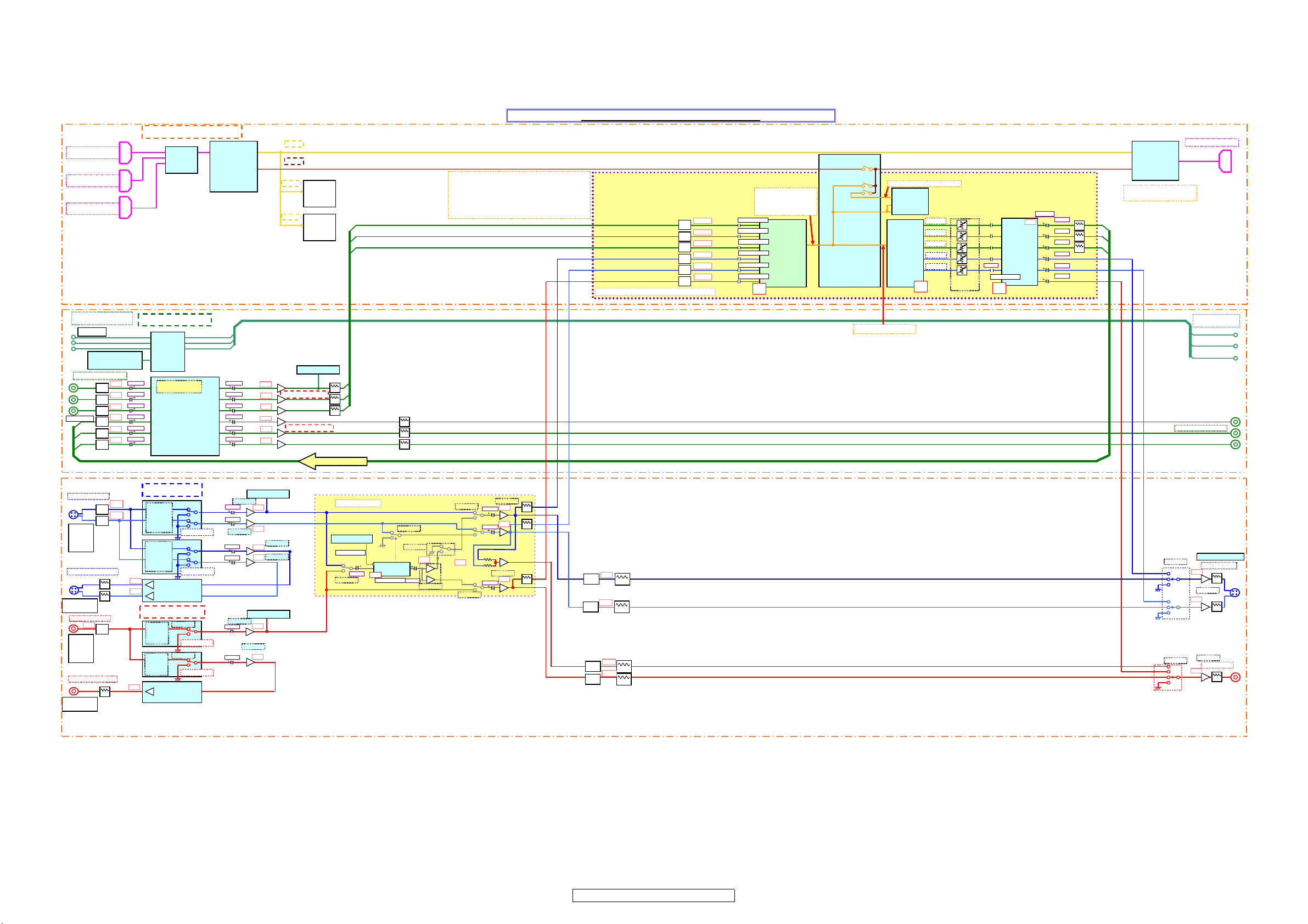
VIDEO BLOCK DIAGRAM
㪠㪚㪈㪇㪈㪇
㩿㪧㪣㪛㪀
㪜㪧㪤㪌㪎㪇㪝
㪉㪌㪍䌃㪌䌎
(
)
(
)
72%108'465+)0#.
K
㪘㪻㫁㫌㫊㫋㫄㪼㫅㫋
㪹㫃㫆㫋㫋㫀㫅㪾㩷㫆㫌㫋
䇮
DIGITAL VIDEO
HDMI-1
HDMI -2
HDMI -3
IC1002
HDMI
SW
SiI9185
IC1008
RECEIVER
SiI9135
Audio
Video
I2s
SPDIF
To DSP
To DIR
AtoH CONVERT specification
1.480i㸢480i/480p/1080i60Hz/720p60Hz/1080p60Hz
2.576i㸢576i/576p/1080i50Hz/720p50Hz/1080p50Hz
3.480p㸢1080i60Hz/720p60Hz/1080p60Hz
4.576p㸢1080i50Hz/720p50Hz/1080p50Hz
5.1080i60Hz/720p60Hz㸢1080p60Hz
6.1080i50Hz/720p50Hz㸢1080p50Hz
AVR-1909 VIDEO BLOCK DIAGRAM
75ƻ
LOAD
75ƻ
LOAD
75ƻ
LOAD
75ƻ
LOAD
75ƻ
LOAD
75ƻ
VIDEO CONVERT BLOCK
LOAD
-6dB
-6dB
-6dB
-6dB
-6dB
-7.7dB
INPUT:1.0Vpp
INPUT:0.7Vpp
INPUT:0.7Vpp
INPUT:1.0Vpp
INPUT:0.286Vp
INPUT:0.82Vpp
PS/HD:YCBCR4:2:2
16bit
SD:ITU-R656 8bit
IC1020
VIDEO
DECODER
ADV7401
70㷄
HDMI
IC1009
TRANSMITTER
SiI9134
PS/HD:YCBCR4:2:2 16bit
IC1011
I/P
SCALER
FLI2310
DAC D
DAC E
IC1019
DAC F
VIDEO
ENCODER
ADV7172
DAC B
DAC C
70㷄
㪽㪺㪑㪎㪐㪅㪍㪟㫑
BH7868FS
INPUT:1Vpp
70㷄
IC1018
FILTER
internal
VIDEO
DRIVER
1000u
㪽㪺㪑㪈㪅㪇㪍㪟㫑
6dB
㪽㪺㪑㪊㪅㪉㪈㪟㫑
㪽㪺㪑㪊㪅㪉㪈㪟㫑
㪽㪺㪑㪈㪅㪇㪍㪟㫑
㪽㪺㪑㪊㪅㪉㪈㪟㫑
㪽㪺㪑㪈㪅㪇㪍㪟㫑
㪎㪌㱅
㪎㪌㱅
㪎㪌㱅
㪰㪚㪙㪚㪩㸢㪩㪞㪙
㪛㪘㪫㪘㩷㪩㪘㪥㪞㪜㩷㫀㫊㩷㪼㫏㪺㫌㫋㪼㪻㩷㫎㫀㫋㪿㩷㪫㫏
D CONTROL IN
JAPAN ONLY
㪛㩷㪠㪥㪧㪬㪫㩷㫏㪉
DC GENERATOR
COMPONENT/D IN
LOAD
LOAD
LOAD
㪠㪥㪧㪬㪫㩷㫏㪊
LOAD
LOAD
LOAD
S(Y/C) IN
LOAD
LOAD
㪠㪥㪧㪬㪫㩷㫏㪊
S(Y/C) RECOUT
㪦㪬㪫㪧㪬㪫㩷㫏㪈
-6dB
LOAD
㪠㪥㪧㪬㪫㩷㫏㪊
CVBS RECOUT
㪦㪬㪫㪧㪬㪫㩷㫏㪈
75ƻ
75ƻ
75ƻ
75ƻ
75ƻ
75ƻ
75ƻ
75ƻ
75ƻ
㪎㪌㱅
㪎㪌㱅
㪎㪌㱅
LINE3
-6dB
-6dB
-6dB
-6dB
-6dB
-6dB
-6dB
-6dB
COMPONENT
IC2027,
IC2026
INPUT
SELECTOR
㪽㪺㪑㪇㪅㪇㪈㪍㪟㫑
㪽㪺㪑㪇㪅㪇㪈㪍㪟㫑
㪽㪺㪑㪇㪅㪇㪈㪍㪟㫑
㪽㪺㪑㪇㪅㪇㪈㪍㪟㫑
㪽㪺㪑㪇㪅㪇㪈㪍㪟㫑
㪽㪺㪑㪇㪅㪇㪈㪍㪟㫑
S-VIDEO
IC2002/IC200
3
INPUT
SELE
CTOR
IC2009/2010
REC
SELE
CTOR
6dB
IC2016
RECOUT
6dB
BUFFER/INH
CONPOSITE
INPUT
SELE
CTOR
REC
SELE
CTOR
IC2016
6dB
RECOUT
BUFFER/INH
INTERNAL
GAIN:0dB
IC2023
INPUT
SELECTOR
NJW1321
INPUT MUTE
INPUT MUTE
IC2004
INPUT
SELECTOR
INPUT MUTE
IC2011
INPUT MUTE
㪽㪺㪑㪇㪅㪇㪈㪍㪟㫑
㪽㪺㪑㪇㪅㪇㪈㪍㪟㫑
㪽㪺㪑㪇㪅㪇㪈㪍㪟㫑
㪽㪺㪑㪇㪅㪇㪈㪍㪟㫑
㪽㪺㪑㪇㪅㪇㪈㪍㪟㫑
㪽㪺㪑㪇㪅㪇㪈㪍㪟㫑
㪽㪺㪑㪇㪅㪈㪍㪟㫑
㪽㪺㪑㪇㪅㪈㪍㪟㫑
IC2005
㪽㪺㪑㪇㪅㪈㪍㪟㫑
㪽㪺㪑㪇㪅㪈㪍㪟㫑
IC2008
㪽㪺㪑㪇㪅㪈㪍㪟㫑
IC2001
IC2008
6dB
6dB
6dB
6dB
6dB
SIGNAL DET.
6dB
6dB
IC2001
0dB
0dB
IC2005
SIGNAL DET.
6dB㪽㪺㪑㪇㪅㪈㪍㪟㫑
0dB
SIGNAL DET.
IC2021NJM2581
IC2022NJM2581
㪎㪌㱅
㪎㪌㱅
㪎㪌㱅
OSD BLOC
SYNC. DET.
INPUT:2Vpp
IC2007
㪽㪺㪑㪇㪅㪈㪌㪟㫑
70㷄
IC2017
OSD
INPUT:2Vpp
㪎㪌㱅
㪎㪌㱅
㪎㪌㱅
IC2007
IC2007
㪽㪺㪑㪇㪅㪈㪍㪟㫑
0dB
IC2018
IC2008
0dB
IC2008
㪽㪺㪑㪇㪅㪈㪍㪟㫑
㪽㪺㪑㪇㪅㪈㪍㪟㫑
㪽㪺㪑㪇㪅㪈㪍㪟㫑
IC2012
0dB
0dB
IC2013
0dB
D CONTROL OUT
SD:ITU-R656 ONLY
㪎㪌㱅
㪎㪌㱅
IC2014
-6dB
㪎㪌㱅
330ƻ
LOAD
330ƻ
LOAD
330ƻ
LOAD
330ƻ
LOAD
㪊㪊㪇㱅
-6dB
㪊㪊㪇㱅
-6dB
㪊㪊㪇㱅
-6dB
㪊㪊㪇㱅
IC2015
JAPAN ONLY
S MONI.DET.
S(Y/C) OUT
6dB
IC2016
6dB
IC2016
CVBS OUT
6dB
㪎㪌㱅
㪎㪌㱅
㪎㪌㱅
33
AVR-1909/789, AVC-1909
Page 34

LEVEL DIAGRAMS (1/5)
-2dB
-35dB
+28dB
DSP
-2+2=0dB
NON CLICP MAX SIGNAL LEVEL 4.0Vrms
Config2˴DOLB Y LIMIT LEVEL 1.41 Vrms (ALLch-3dBFS)
-2+6.5=4.5dB
SUM FROM SWch
Config1˴DOLB Y LIMIT LEVEL (ALLc h-3dBFS)
3.876V
FRONT LEVEL DIAGRAM
R2A15215FP
LINE IN
㧗
㧗 㧙
TO
Surround Back
(ZONE2 MODE)
AVR-1909
LEVEL DIAGRAM
FRONT ch
ANALOG
ATT
㧗
GAIN
ADJ.
A/D
ADAU1328
D/A
㧙
FROM SWch
㧙
D/A OUT
MUTE
㧙
㧗
㧙
㧙
H/POUT
SPEAKER
OUT
EXT IN
200mV
+20dB
+10dB
˴0dB
-10dB
-20dB
㧗
LINE IN/EXT IN
-8dB
ADAU1328
-10dBFS
-20dBFS
-30dBFS
0dBFS
A/D IN
79.4mVrms
0dBFS
0.88Vrms
-10dBFS
-20dBFS(DIG.IN)
PCM or DD Config1
-22dBFS(A/D IN)
-20dBFS
-26.5dBFS(DIG.IN)
˴DD Config2
-30dBFS
0dBFS
+7dB
RECOUT
+30dB
SP OUT
3.99Vrms/8Ω
+20dB
+10dB
RECOUT
˴0dB
-10dB
H/POUT
71.0mVrms
-20dB
-30dB
-40dB
-40dBFS
-40dBFS
-30dB
-40dB
34
AVR-1909/789, AVC-1909
Page 35

LEVEL DIAGRAMS (2/5)
-2dB
+29dB
-2+2=0dB
NON CLICP MAX SIGNAL LEVEL 4.0Vrms
Config2˴DOLB Y LIMIT LEVEL (ALLc h-3dBFS)
-2+6.5=4.5dB
Config1˴DOLB Y LIMIT LEVEL (ALLc h-3dBFS)
DSP
CENTER LEVEL DIAGRAM
AVR-1909
LEVEL DIAGRAM
CENTER ch
R2A15215FP
EXT IN
200mV
+20dB
+10dB
˴0dB
-10dB
-20dB
㧗
LINE IN/EXT IN
㧗
GAIN
ADJ.
A/D
ADAU1328
0dBFS
0.88Vrms
-20dBFS(DIG.IN)
PCM or DD Config1
-22dBFS(A/D IN)
-26.5dBFS(DIG.IN)
˴DD Config2
D/A
0dBFS
-10dBFS
-20dBFS
-30dBFS
㧗
+7dB
㧙
D/A OUT
MUTE
㧗
㧙
SPEAKER
OUT
+30dB
SP OUT
3.99Vrms/8Ω
+20dB
+10dB
˴0dB
-10dB
-20dB
-30dB
-40dB
-40dBFS
-30dB
-40dB
35
AVR-1909/789, AVC-1909
Page 36

LEVEL DIAGRAMS (3/5)
-2dB
PLD
DSP
NON CLICP MAX SIGNAL LEVEL 4.0Vrms
Config2˴DOLB Y LIMIT LEVEL (ALLc h-3dBFS)
-2+(20-6)=12dB
Config1˴DOLB Y LIMIT LEVEL˴(ALLch- 3dBFS)
3.876V
SUM to FRONTch
SUB WOOFER LEVEL DIAGRAM
AVR-1909
LEVEL DIAGRAM
SUBWOOFER ch
R2A15215FP
EXT IN
200mV
+20dB
+10dB
˴0dB
-10dB
-20dB
-30dB
-40dB
㧗
LINE IN/EXT IN
㧗
A/D
ADAU1328
㧙
ADAU1328
0dBFS
0.88Vrms
-10dBFS
-20dBFS
-34dBFS(PCM.IN)
-36dBFS(A/D IN)
-30dBFS
-40dBFS(DIG.IN)
˴DD Config1
-40dBFS
-46.5dBFS(DIG.IN)
˴DD Config2
-50dBFS
D/A
0dBFS
㧙
GAIN
㧗
+7dB
㧙
㧙㧙㧙
+6dB
D/A OUT
MUTE
+3dB
SUM to FRONT-ch
ADJ.
PREOUTMUTE
+30dB
+20dB
+10dB
PREOUT
317mVrms
˴0dB
PREOUT
159mVrms
-10dB
-20dB
-30dB
-40dB
36
AVR-1909/789, AVC-1909
Page 37

LEVEL DIAGRAMS (4/5)
-2dB
+28dB
-2+2=0dB
NON CLICP MAX SIGNAL LEVEL 4.0Vrms
Config2˴DOLB Y LIMIT LEVEL 1.41 Vrms(ALLch-3dBFS)
-2+6.5=4.5dB
Config1˴DOLB Y LIMIT LEVEL 1.41 Vrms(ALLch-3dBFS)
DSP
SURROUND LEVEL DIAGRAM
AVR-1909
LEVEL DIAGRAM
SURROUND ch
R2A15215FP
EXT IN
+20dB
+10dB
㧗
GAIN
ADJ.
A/D
ADAU1328
0dBFS
0.88Vrms
D/A
0dBFS
㧗
㧙
D/A OUT
MUTE
㧗
㧙
㧗
SPEAKER
OUT
+30dB
SP OUT
3.99Vrms/8Ω
+20dB
+10dB
200mV
˴0dB
-10dB
-20dB
-30dB
-40dB
LINE IN/EXT IN
-10dBFS
-23dBFS(DIG.IN)
PCM or DD Config1
-25dBFS(A/D IN)
-20dBFS
-29.5dBFS(DIG.IN)
˴DD Config2
-30dBFS
-40dBFS
+10dB
37
AVR-1909/789, AVC-1909
˴0dB
-10dB
-20dB
-30dB
-40dB
Page 38

LEVEL DIAGRAMS (5/5)
-2dB
+26dB
-2+3+2=+3dB
NON CLICP MAX SIGNAL LEVEL 4.0Vrms
Config2˴DOLB Y LIMIT LEVEL 1.41 Vrms (ALLch-3dBFS)
-2+3=1dB
Config1˴DOLB Y LIMIT LEVEL 1.41 Vrms (ALLch-3dBFS)
-2+6.5+3=7.5dB
DSP
SURROUND BACK LEVEL DIAGRAM
AVR-1909
LEVEL DIAGRAM
SURR.BACK ch
R2A15215FP
EXT IN
200mV
+20dB
+10dB
˴0dB
-10dB
-20dB
-30dB
㧗
LINE IN/EXT IN
㧗
GAIN
ADJ.
A/D
ADAU1328
0dBFS
0.88Vrms
-25dBFS(A/D IN)
-26dBFS(DIG.IN)
DD EX Config1
-32.5dBFS(DIG.IN)
DD EX Config2
D/A
0dBFS
-10dBFS
-20dBFS
-30dBFS
-40dBFS
㧗
+7dB
㧙
D/A OUT
MUTE
㧗
㧙
SPEAKER
OUT
+30dB
SP OUT
3.99Vrms/8Ω
SP OUT(D/A OUT)
2.82Vrms/8Ω
+20dB
+10dB
˴0dB
-10dB
-20dB
-30dB
-40dB
-40dB
38
AVR-1909/789, AVC-1909
Page 39

SEMICONDUCTORS
Only major semiconductors are shown, general semiconductors etc. are omitted to list.
主な半導体を記載しています。汎用の半導体は記載を省略しています。
1. IC’s
M30879FLBFP (IC802)
P0_7/AN0_7/D7
P0_6/AN0_6/D6
P0_5/AN0_5/D5
P0_4/AN0_4/D4
P0_3/AN0_3/D3
P0_2/AN0_2/D2
P0_1/AN0_1/D1
P0_0/AN0_0/D0
P10_7/AN7/KI3
P10_6/AN6/KI2
P10_5/AN5/KI1
P10_4/AN4/KI0
P10_3/AN3
P10_2/AN2
P10_1/AN1
AVSS
P10_0/AN0
VREF
P9_7/ADTRG/SIN4
AVCC
NOTES:
1. P7_0 and P7_1 are N channel open-drain output pins.
P2_7/AN2_7/A7(/D7/D6)
P2_0/AN2_0/A0(/D0/-)
P1_7/D15/INT5
P1_0/D8
P1_1/D9
81
82
83
84
85
86
87
88
89
90
91
92
93
94
95
96
97
98
99
00
1
1 2 3 4 5 6 7 8 9 101112131415161718192021222324252627282930
P1_2/D10
P1_3/D11
P1_4/D12
P1_5/D13/INT3
P2_1/AN2_1/A1(/D1/D0)
P1_6/D14/INT4
BYTE
CNVSS
P8_7/XCIN
P9_4/DA1/TB4IN
P9_3/DA0/TB3IN
P9_1/TB1IN/SIN3
P9_5/ANEX0/CLK4
P9_6/ANEX1/SOUT4
P9_0/TB0IN/CLK3
P9_2/TB2IN/SOUT3
P2_5/AN2_5/A5(/D5/D4)
P2_6/AN2_6/A6(/D6/D5)
P2_4/AN2_4/A4(/D4/D3)
P2_2/AN2_2/A2(/D2/D1)
P2_3/AN2_3/A3(/D3/D2)
VCC2
P3_0/A8(/-/D7)
VSS
M30626FHPFP
XIN
VSS
VCC1
XOUT
RESET
P8_6/XCOUT
P8_5/NMI
P8_3/INT1
P8_4/INT2/ZP
P3_1/A9
P3_2/A10
P8_2/INT0
P8_1/TA4IN/U
P3_6/A14
P3_3/A11
P8_0/TA4OUT/U
P3_7/A15
P3_4/A12
P3_5/A13
P7_7/TA3IN
P7_6/TA3OUT
P7_5/TA2IN/W
P7_4/TA2OUT/W
P4_0/A16
P4_1/A17
P4_2/A18
P4_3/A19
515253545556575859606162636465666768697071727374757677787980
50
P4_4/CS0
49
P4_5/CS1
48
P4_6/CS2
47
P4_7/CS3
46
P5_0/WRL/WR
45
P5_1/WRH/BHE
44
P5_2/RD
43
P5_3/BCLK
42
P5_4/HLDA
41
P5_5/HOLD
40
39
38
37
36
35
34
33
32
31
(1)
(1)
P5_6/ALE
P5_7/RDY/CLKOUT
P6_0/CTS0/RTS0
P6_1/CLK0
P6_2/RXD0/SCL0
P6_3/TXD0/SDA0
P6_4/CTS1/RTS1/CTS0/CLKS1
P6_5/CLK1
P6_6/RXD1/SCL1
P6_7/TXD1/SDA1
P7_2/CLK2/TA1OUT/V
P7_3/CTS2/RTS2/TA1IN/V
P7_0/TXD2/SDA2/TA0OUT
P7_1/RXD2/SCL2/TA0IN/TB5IN
M30879FLBFP Terminal Function
Pin Pin Name Symbol I/O Type Det
1 P96/TXD4 SIRIUS TXD O C - - - Z O/L O/L SIRIUS control pin
2 P95/CLK4 MICDET I - Lv - Eu Z O/L O/L Microphone detect input (Detected : H)
3 P94/TB4 H/PDET I - Lv - Eu Z O/L O/L HEADPHONE detect input (Detected : H)
4 P93/TB3 FL_DATA O C - - Z O/L O/L FLD DRIVER control pin
5P92/
SOUT3
MOSI O C - - Ed Z O/L O/L
6 P91/SIN3 SOMIm I - Lv - - Z I O/L
7 P90/CLK3 CLKMO O C - - Ed Z O/L O/L
8BYTE BYTE I - - - - - - -
9 CNVCS CNVSS I - - - Ed Z I I UP GRADE PIN
10 P87 FL_RST O C - - Z O/L O/L FLD DRIVER Reset control pin
11 P86 GRNLED O C - - - Z O/L O/L STBYLED GREEN control pin
12 RESET RESET
I - Lv - Eu L I I u-COM RESET SIGNAL INPUT
13 XOUT XOUT O - - - - - O/L O/L OSILATOR CONNECTION
14 VSS VSS - - - - - - - - GND
15 XIN XIN I - - - - - I I OSILATOR CONNECTION
Op
(Int.)Op(Ext.)
Res Stby Stop Function
MAIN-SUBμcom comm. control pin
MAIN-SUBμcom comm. control pin
MAIN-SUB μcom comm. control pin
MAIN-SUB μcom comm. control pin
39
AVR-1909/789, AVC-1909
Page 40

Pin Pin Name Symbol I/O Type Det
16 VCC VCC - - - - - - - - POWER 5V
17 P85/NMI NMI I - - - - - - - 5V
18 P84/INT2 PROTECTION
19 P83/INT1 POWERKEY
20 P82/INT0 REMOTEDET I - Lv - Ed Z O/L O/L ROOM TO ROOM Signal detect pin (Detected : H)
21 P81 ISELB I - - - Eu Z O/L O/L Input selector rotation detect input (Rotary
22 P80 VSELA I - - - Eu Z O/L O/L Master Volume rotation detect input (Rotary
23 P77 SSELA I - - - Eu Z O/L O/L Selector rotation detect input (Rotary encoder)
24 P76 - O C - - - Z O/L O/L Not used
25 P75 HD AUDIO LED O C - - - Z O/L O/L HD AUDIO LED control
26 P74 SSELB I - - - Eu Z O/L O/L Selector rotation detect input (Rotary encoder)
27 P73/CTS2 VOLDATA O C - - - Z O/L O/L Volume control pin
28 P72/CLK2 VOLCLK O C - - - Z O/L O/L Volume control pin
29 P71/RXD2 RXDMIXO I - - - Ed Z I O/L XM RADIO control pin
30 P70/TXD2 TXDMOXMI O N - - Eu Z O/L O/L XM RADIO control pin
31 P67/TXD1 MO232CI O C - - - Z O/L O/L RS232C SIGNAL OUTPUT
32 P66/RXD1 MI232CO I - - - Ed Z I O/L RS232C SIGNAL INPUT
33 P65/CLK1 EXPCLK O C - - - Z O/L O/L Extended IC control pin
34 P64/CTS1 EXPDATA O C - - - Z O/L O/L Extended IC control pin
35 P63/TXD0 MOIPI O C - - - Z O/L O/L iPod control pin
36 P62/RXD0 MIIPO I - - - Ed Z I O/L iPod control pin
37 P61/CLK0 VSELB I - - - Eu Z O/L O/L Master Volume rotation detect input (Rotary
38 P60/CTS0 ISELA I - - - Eu Z O/L O/L Input selector rotation detect input (Rotary
39 P57 REDLED O C - - - Z O/H O/L STBY LED RED CONTROL
40 P56 FL_CE1 O C - - Z O/L O/L FLD DRIVER control pin
41 P55/EPM FRASH CE/FL_CLK O C - - - Z O/L O/L Rewrite boot program start : L input set
42 P54 M232CPOWER O C - - Ed Z O/L O/L RS232C POWER control pin (STANDBY:H)
43 P53 DYN GRN LED O C - - - Z O/L O/L DYNAMIC VOLUME LED GREEN control
44 P52 DYN RED LED O C - - - Z O/L O/L DYNAMIC VOLUME LED RED control
45 P51 TRIGGER1 O C - - - Z O/L O/L TRIGGER OUT 1 control pin
46 P50/CE FRASH CE O C - - - Z O/L O/L Rewrite boot program start : H input set
47 P47 RDSDOUT I - - - Eu Z O/L O/L RDS DETECT IN control pin
48 P46 TURDSCLK(CKTU) O C - - - Z O/L O/L TUNER/RDS CLOCK OUT
49 P45 TURDSDATA(DATATU) O C - - - Z O/L O/L TUNER/RDS DATA OUT control pin
50 P44 RDSCE O C - - - Z O/L O/L RDS Chip enable
51 P43 RDSRST O C - - - Z O/L O/L RDS reset output
52 P42 THERMAL
53 P41 EXPOE O C - - - Z O/L O/L Extended IC control pin
54 P40 EXPSTB O C - - - Z O/L O/L Extended IC control pin
55 P37 TUDOUT(DATAOUT) I - Lv - Ed Z O/L O/L TUNING DATA INPUT control pin
56 P36 TUSTB O C - - - Z O/L O/L TUNER STB OUT
57 P35 STEREO I - Lv - Eu Z O/L O/L When TUNER FM stereo receive : L
58 P34 TUNED I - Lv - Eu Z O/L O/L TUNER turned detect (Detected : L)
59 P33 IPDET I - Lv - Eu Z O/L O/L MINI JACK connected detection pin for DOCK
60 P32 REMOTEPOWER O C - - - Z O/L O/L REMOTE POWER control pin (ON : H)
61 P31 232C CONTROL O C - - Ed Z O/L O/L 232C control pin (MAIN : L / SUB : H)
62 VCC VCC - - - - - - - - +5V
63 P30 VOLPROTECT
64 VSS VSS - - - - - - - - GND
65 P27 PRE POWER O C - - - Z O/L O/L PRE POWER control pin (H : ON)
66 P26 SCPUPOWER O C - - - Z O/L O/L SUB CPU POWER ON/OFF switcing (H : ON)
67 P25 XMPOWER O C - - - Z O/L O/L XM RADIO POWER control pin
68 P24 POWER O C - - Ed Z O/L O/L MAIN POWER relay control output (ON : H)
69 P23 CPU/EPOWER O C - - Ed Z O/L O/L MAIN CPU POWER control pin (POWER ON : H)
70 P22 LIMIT O C - - - Z O/L O/L LIMIT control
71 P21 - O C - - - Z O/L O/L Not used
72 P20 - O C - - - Z O/L O/L Not used
73 P17/INT5 REMOCOM I 74 P16/INT4 REQSOMIm I 75 P15/INT3 B.DOWN
76 P14/D12 RST SUB O C - - - Z O/L O/L
I-
I - Lv - Eu Z I I MAIN POWER relay control output
I - - - Ed Z O/L O/L Temperature detect
I-
I-
E ↓ &L
E ↑ &H
E ↑ &H
E ↓ &L
E ↓ &L
Op
(Int.)Op(Ext.)
- Eu Z I I PROTECTION SIGNAL INPUT
- Eu Z O/L O/L Voltage detection control pin
- Ed Z I I Remote control signal input
- Ed Z I O/L MAIN-SUB Éþcom comm. control pin
- Eu Z I I Power down detect (Power down : L)
Res Stby Stop Function
encoder)
encoder)
encoder)
encoder)
/FLD DRIVER control pin
connection (H:DETECTIVE)
SUB μcom Reset control pin
40
AVR-1909/789, AVC-1909
Page 41

Pin Pin Name Symbol I/O Type Det
77 P13/D11 LIMITDET I - Lv - Eu Z O/L O/L Signal detect input (Detected : H)
78 P12/D10 - O C - - Ed O/L O/L Not used
79 P11/D9 - O C - - - - O/L O/L Not used
80 P10/D8 VOLMUTE O C - - - Z O/L O/L VOLUME MUTE control pin
81 P07/D7 MUTEPOWER O C - - - Z O/L O/L For MUTE +B control pin
82 P06/D6 SYNCDET I - Lv - Ed Z O/L O/L Sync. detect input for MAIN(H: Ext. synchronized)
83 P05/D5 OSDMUTE O C - - - Z O/L O/L OSD control pin
84 P04/D4 - O C - - - Z O/L O/L Not used
85 P03/D3 OSDRST O C - - - Z O/L O/L OSD control pin
86 P02/D2 OSDSTR O C - - - Z O/L O/L OSD control pin
87 P01/D1 OSDCLK O C - - - Z O/L O/L OSD control pin
88 P00/D0 OSDDATA O C - - - Z O/L O/L OSD control pin
89 P103/AN3 KEY1 I - Lv - Eu Z O/L O/L KEY1 SIGNAL INPUT
90 P102/AN2 KEY2 I - Lv - Eu Z O/L O/L KEY2 SIGNAL INPUT
91 P101/AN1 KEY3 I - Lv - Eu Z O/L O/L KEY3 SIGNAL INPUT
92 P104/AN4 ACKSUB O C - - Ed Z O/L O/L
93 P107/AN7 XMOLINKACTIVE I - - - Ed Z O/L O/L XM RADIO control pin
94 P106/AN6 XMOANTREV I 95 P105/AN5 XMIRESET O C - - Eu Z O/L O/L XM RADIO RESET control pin
96 AVS S AV SS - - - - - - - - G ND
97 P100/AN0 SET_OPTION I - Lv - - Z O/L O/L SET OPTION SELECT
98 VREF VREF - - - - - - - - VREF
99 AVCC AVCC - - - - - - - - POWER 5V
100 P97/RXD4 SIRIUS RXD I - - - Ed Z O/L O/L SIRIUS control pin
E ↓ &L
Op
(Int.)Op(Ext.)
- Ed Z O/L O/L XM RADIO control pin
Res Stby Stop Function
MAIN-SUB μcom comm. control pin
Note: Pin No. : Terminal number of microcomputer.
Port Name : The name entered in the data sheet of microcomputer.
Symbol : Symbolized interface function.
I/O : Input or out of part.
“I” = Input port
“O” = Output port
Type : Composition of port in case of output port.
“C” = CMOS output
“N” = NMOS open drain output
“P” = PMOS open drain output
Op : Pull up/Pull down selection information.
“Iu” = Inner microcomputer pull up
“Id” = Inner microcomputer pull down
“Eu” = External microcomputer pull up
“Ed” = External microcomputer pull down
Det : Indicates judging state of input port. Level detection is “LV”; Edge detection is “Ed”; Detection by both shifting is “E&L”;
Serial data detection is “S” (Serial data output is also “S”).
Res : State at reset.
“H” = Outputs High Level at reset
“L” = Outputs Low Level at reset
“Z” = Becomes High impedance mode at reset
STBY : State of port when STANDBY mode.
“O/L” = Output port and “L”
“I” = Input port
Stop : State of port when Stop mode.
“O/L” = Output port and “L”
“I” = Input port
41
AVR-1909/789, AVC-1909
Page 42

M3062LFGPGP (IC1405)
M3062LFGPGP Terminal Function
Pin Pin Name Symbol I/O Type Det
1 P94/TB4 VPLD DATA O C - - - Z VIDEO PLD control pin
2 P93/TB3 DIR CE O C - - - Z DIR control pin(LC89057W-VF4A)
3 P92/SOUT3 DIR DIN O C - - - Z DIR control pin(LC89057W-VF4A)
4 P91/SIN3 DIR DOUT I - Lv - Eu Z DIR control pin(LC89057W-VF4A)
5 P90/CLK3 DIR CLK O C - - - Z DIR control pin(LC89057W-VF4A)
6 BYTE BYTE - - - - - - GND(Ext. data bus bit width switching, 16bit:L)
7 CNVCS CNVSS - - - - - - Single-chip/Micro-processor mode switching(Normal single-chip:L,
8 P87 VERST O C - - Eu Z Reset for VIDEO ENCODER(ADV7172)
9 P86 VDRST O C - - Eu Z Reset for VIDEO DECODER(ADV7401)
10 RESET SUBRESET
11 XOUT X1 O - - - - - Oscillator connection
12 VSS VSS - - - - - - GND
13 XIN X2 I - - - - - Oscillator connection
14 VCC VCC - - - - - +3.3V
15 P85/NMI NMI I - - - - - Not used(Fixed to H)
16 P84/INT2 CEC_IN I 17 P83/INT1 ACKSIMO I -
18 P82/INT0 SUB BDOWN
19 P81 IP RST O C - - - Z IP CONV(FLI2310) reset
20 P80 - I - - - Ed Z Not used
21 P77 SICODECO I - - - - Z CODEC (ADAU1328) control pin
22 P76 CPU_MUTE/TMS O C - - - Z MAIN PLD DAC MUTE control pin/PLD rewrite control(JTAG)
23 P75 APLDSEL1/TDI O C - - - Z MAIN PLD control pin/PLD rewrite control(JTAG)
I - Lv - Eu L Reset input
E ↓ &L
E ↓ &L
I-
E ↓ &L
Op
(Int.)Op(Ext.)
- Eu Z CEC-D signal input pin
-EdZ
Res Function
Rewrite boot program start:H input set)
MAIN-SUBμcom comm. control input pin("L" return from MAIN
μcom)
Eu Z Power down detect(Power down:L)
42
AVR-1909/789, AVC-1909
Page 43

Pin Pin Name Symbol I/O Type Det
24 P74 MTCK O C - - - Z PLD rewrite control(JTAG)
25 P73/CTS2 VIDEO_POWER O C - - - Z VIDEO Power ON/OFF switching(H:ON)
26 P72/CLK2 DAC_POWER O C - - Ed Z DIGITAL Power ON/OFF switching(H:ON)
27 P71/RXD2 VSCL I/O N - - Eu Z VIDEO I2C- IP CONV(FLI2310)/V_ENCODER(ADV7172)/
28 P70/TXD2 VSDA I/O N - - Eu Z VIDEO I2C- IP CONV(FLI2310)/V_ENCODER(ADV7172)/
29 P67/TXD1 TXD O C - - Eu Z Data transmission output to outside
30 P66/RXD1 RXD I - Lv - Eu Z Data transmission input from outside
31 P65/CLK1 SW SUM O C - - Ed Z Additional instructions to Front of an SW signal(H:ON)
32 P64/CTS1 HDMIPOWER O C - - Z HDMI POWER control pin(H:ON)
33 P63/TXD0 SOMI O C - - - Z
34 P62/RXD0 SIMO I - - - Ed Z
35 P61/CLK0 CLKSIMO I - - - Ed Z
36 P60/CTS0 REQSOMI O C - - Ed Z
37 P57 1TMDSSWRST O C - - - Z SiI9185 Reset pin
38 P56 HDP2 O C - - - Z HD DET control pin
39 P55/EPM ADPDOWN/AUTH I C - - Ed Z Rewrite boot program start : L input set
40 P54 CEC_OUT O C - - - Z CEC-D signal output pin
41 P53 MONIDIS O C - - Z COMPONENT MONITOR OUT output control pin
42 P52 VCR2INH (CDR) O C - - - Z Not used
43 P51 VCR1INH (VCR) O C - - - Z VCR1OUT output INH control (L:MUTE)
44 P50/CE WP4/(AVMUTE) O/I - - - Eu Z Write Protect control / Rerite boot program start : H input set
45 P47 HS_INT I 46 P46 DSPPWR O C - - Ed Z H:DSP Power ON
47 P45 HDP1 O C - - Ed Z HP DET control pin
48 P44 P.SAVE O - - - Ed Z COMPONENT CONVERT output control pin
49 P43 HRINT I C
50 P42 HSCL/EDID SCL I/O C - - Eu Z VIDEO I2C/HDMI EDIT(E2PROM) control pin
51 P41 HSDA/EDID SDA I/O C - - Eu Z VIDEO I2C/HDMI EDIT(E2PROM) control pin
52 P40 Z1SMONIA O C - - Z Z1 SMONITOR select
53 P37 HDMIR_RST O C - - Eu Z Reset for HDMI RECEIVER(SiI9135)
54 P36 1HTRST O C - - Eu Z Reset for HDMI TRANSMITTER1
55 P35 Z1SMONIB O C - - Ed Z Z1 SMONITOR select
56 P34 1HTINT I - Lv - . Z HDMI OUT signal detect input(HDMI TRANS1 SiI9134)
57 P33 PAL/NTSC O - - - Ed Z Not used
58 P32 SOCODECI O C - - - Z CODEC (ADAU1328) control pin
59 P31 CLKCODEC O C - - - Z CODEC (ADAU1328) control pin
60 VCC VCC - - - - - - +3.3V
61 P30 CECODEC O C - - - Z CODEC (ADAU1328) control pin
62 VSS VSS - - - - - - GND
63 P27 CODECRST O C - - - Z CODEC (ADAU1328) control pin
64 P26 XMDACRST O C - - - Z XMDAC control pin (AK4385)
65 P25 XMDACCS O C - - - Z XMDAC control pin (AK4385)
66 P24 XMDACMC O C - - - Z XMDAC control pin (AK4385)
67 P23 XMDACMDI O C - - - Z XMDAC control pin (AK4385)
68 P22 VEXPSTB O C - - - Z Terminal output for VIDEO expander control(BU4094BCFV)
69 P21 VEXPOE O C - - Ed Z Terminal output for VIDEO expander control(BU4094BCFV)
70 P20 VEXPCLK O C - - - Z CLK output for VIDEO expander control(BU4094BCFV)
71 P17/INT5 VEXPDIN O C - - - Z DATA output for VIDEO expander control(BU4094BCFV)
72 P16/INT4 COMPSDET I - Lv - Eu Z COMPONENT IN signal detect input
73 P15/INT3 Z1VSIG.DET I - Lv - Eu Z VIDEO IN signal detect input (Signal inputted : H)
74 P14/D12 Z1SMONIDET I - - - Eu Z S MONITER connection existence detection input (connected:L)
75 P13/D11 Z1SSIGDET I - - - Eu Z S signal detect input (signal inputted:H)
76 P12/D10 SYNCDET I - Lv - - Z SyncDet pin
77 P11/D9 CPUCONT O C - - - - A.PLD Control Bit
78 P10/D8 D.POWER O C - - Ed Z Digital Power ON/OFF control pin
79 P07/D7 PLDWRITE O C - - - Z PLD JTAGLINE ON/OFF control
80 P06/D6 VPLDCE/TDO O/I - - - Ed Z VIDEO PLD control pin/PLD rewrite control (JTAG)
81 P05/D5 HDP3 O C - - - Z HP DET control pin
82 P04/D4 HDP4 O C - - - Z HP DET control pin
83 P03/D3 INT1 I - Lv - Eu Z DIR1 control pin
84 P02/D2 INT2 O C - - - Z Not used
85 P01/D1 DIRRST2 O C - - - Z Not used
86 P00/D0 DIRRST1 O C - - - Z DIR1 control pin
E ↓ &L
E ↓ &L
Op
(Int.)Op(Ext.)
- Eu Z HDMI IN SEL(SiI9185) INT output
- - Z HDMI RECEIVER(SiI9031)INT output
Res Function
V_DECODER(ADV7401)/COMPONENT SELECT
IC(NJW1321FP1) control IC
V_DECODER(ADV7401)/COMPONENT SELECT
IC(NJW1321FP1) control IC
MAIN-SUB μcom comm. control pin
MAIN-SUB μcom comm. control pin
MAIN-SUB μcom comm. control pin
MAIN-SUB μcom comm. control pin
43
AVR-1909/789, AVC-1909
Page 44

Pin Pin Name Symbol I/O Type Det
87 P107/AN7 DSPRST O C - - - Z DSP (ADSP-21367) reset output pin (reset:L)
88 P106/AN6 - O C - - - Z Not used
89 P105/AN5 DSPROMRST O C - - Ed Z DSP memory reset(reset:L)
90 P104/AN4 - O C - - - Z Not used
91 P103/AN3 DSPFLAG0 I - Lv - Ed Z DSP control pin (ADSP-21367)
92 P102/AN2 DSPICS O C - Eu Z DSP control pin (ADSP-21367)
93 P101/AN1 DSP FLAG1 I - - - - Z Not used
94 AVS S AVS S - - - - - - AD GN D
95 P100/AN0 VPLDCLK O - - - - Z VIDEO PLD control pin
96 VREF VREF - - - - - - AD ref. +3.3V
97 AVC C AVC C - - - - - - A D +3 . 3V
98 P97/SIN4 DSPMISO I - Lv - Eu Z DSP control pin (ADSP-21367)
99 P96/SOUT4 DSPMOSI O C - - Eu Z DSP control pin (ADSP-21367)
100 P95/CLK4 DSPICLK O C - - Eu Z DSP control pin (ADSP-21367)
Op
(Int.)Op(Ext.)
Res Function
Note: Pin No. : Terminal number of microcomputer.
Port Name : The name entered in the data sheet of microcomputer.
Symbol : Symbolized interface function.
I/O : Input or out of part.
“I” = Input port
“O” = Output port
Type : Composition of port in case of output port.
“C” = CMOS output
“N” = NMOS open drain output
“P” = PMOS open drain output
Op : Pull up/Pull down selection information.
“Iu” = Inner microcomputer pull up
“Id” = Inner microcomputer pull down
“Eu” = External microcomputer pull up
“Ed” = External microcomputer pull down
Det : Indicates judging state of input port. Level detection is “LV”; Edge detection is “Ed”; Detection by both shifting is “E&L”;
Serial data detection is “S” (Serial data output is also “S”).
Res : State at reset.
“H” = Outputs High Level at reset
“L” = Outputs Low Level at reset
“Z” = Becomes High impedance mode at reset
STBY : State of port when STANDBY mode.
“O/L” = Output port and “L”
“I” = Input port
Stop : State of port when Stop mode.
“O/L” = Output port and “L”
“I” = Input port
44
AVR-1909/789, AVC-1909
Page 45

FLI2310 (IC1011)
t
R_VDD
FIELD ID_PORT2
HSYNC_PORT2
VSYNC_PORT2
D1_IN_7
D1_IN_6
D1_IN_5
D1_IN_4
D1_IN_3
D1_IN_2
IN_CLK_PORT2
XTAL IN
XTAL OUT
VDD9
VSS
D1_IN_0
D1_IN_1
VDDcore8
VSScore
TEST0
TEST1
TEST2
R_VDD
R_VSS
R_VSS
R_VDD
R_VSS
R_VDD
R_VDD
R_VSS
Reserved
Reserved
Reserved
R_VSS
R_VSS
Reserved
Reserved
R_VSS
AVDD_PLL_FE
R_VDD1.8
AVDD_PLL_SDI
AVSS_PLL_BE2
AVSS_PLL_FE
AVSS_PLL_SDI
PLL_PVDD
AVDD_PLL_BE2
PLL_PVSS
AVSS_PLL_BE1
AVDD_PLL_BE1
R_VSS
R_VDD
Reserved
HSYNC1_PORT1
VSYNC1_PORT1
FIELD ID1_PORT1
IN_CLK1_PORT1
HSYNC2_PORT1
VSYNC2_PORT1
FIELD ID2_PORT1
VDD1
VSS
IN_CLK2_PORT1
B/Cb/D1_0
B/Cb/D1_1
B/Cb/D1_2
B/Cb/D1_3
B/Cb/D1_4
VDDcore1
VSScore
B/Cb/D1_5
B/Cb/D1_6
B/Cb/D1_7
R/Cr/Cb Cr_0
R/Cr/Cb Cr_1
R/Cr/Cb Cr_2
R/Cr/Cb Cr_3
R/Cr/Cb Cr_4
R/Cr/Cb Cr_5
R/Cr/Cb Cr_6
R/Cr/Cb Cr_7
G/Y/Y_0
VDD2
VSS
G/Y/Y_1
G/Y/Y_2
G/Y/Y_3
G/Y/Y_4
VDDcore2
VSScore
G/Y/Y_5
G/Y/Y_6
G/Y/Y_7
IN_SEL
TEST
DEV_ADDR1
DEV_ADDR0
SCLK
SDATA
RESET_N
VDD3
SDRAM DATA(0)
SDRAM DATA(1)
SDRAM DATA(2)
VSS
1 0 0
1 6 0
1 5 5
1 5 0
1 4 5
1 4 0
1 3 5
1 3 0
1 2 5
1 2 0
1 1 5
1 1 0
1 0 5
OE
G/Y/Y_OUT_7
G/Y/Y_OUT_6
G/Y/Y_OUT_5
G/Y/Y_OUT_4
G/Y/Y_OUT_3
G/Y/Y_OUT_2
G/Y/Y_OUT_1
G/Y/Y_OUT_0
VSS
VDD8
R/V/Pr_OUT_7
R/V/Pr_OUT_6
R/V/Pr_OUT_5
R/V/Pr_OUT_4
R/V/Pr_OUT_3
R/V/Pr_OUT_2
VSScore
VDDcore7
R/V/Pr_OUT_1
R/V/Pr_OUT_0
B/U/Pb_OUT_7
B/U/Pb_OUT_6
B/U/Pb_OUT_5
B/U/Pb_OUT_4
B/U/Pb_OUT_3
B/U/Pb_OUT_2
VSS
VDD7
B/U/Pb_OUT_1
B/U/Pb_OUT_0
CLKOUT
VSScore
VDDcore6
CTLOUT4
CTLOUT3
CTLOUT2
CTLOUT1
CTLOUT0
TEST OUT1
TEST OUT0
TEST3
SDRAM CLKIN
VSS
VDD6
SDRAM CLKOUT
SDRAM DQM
SDRAM CSN
SDRAM BA0
SDRAM BA1
SDRAM CASN
SDRAM RASN
2 0 5
1
2 0 0
1 9 5
1 9 0
1 8 5
1 8 0
1 7 5
1 7 0
1 6 5
5
1 0
1 5
2 0
2 5
3 0
3 5
4 0
4 5
5 0
5 5
6 0
6 5
7 0
7 5
8 0
8 5
9 0
9 5
SDRAM DATA(3)
SDRAM DATA(5)
SDRAM DATA(4)
FLI2310 Block Diagram
Port 2
8-bit
656 Input
Port 1
8/16/24-bit
RGB/YCrCb
Input
Input Processor
with Auto Sync
and auto Adjust
Clock
Generation
PLLs
SDRAM DATA(7)
SDRAM DATA(6)
SDRAM DATA(8)
SDRAM DATA(9)
VSS
VDD4
SDRAM DATA(10)
SDRAM DATA(11)
SDRAM DATA(14)
SDRAM DATA(12)
SDRAM DATA(13)
SDRAM DATA(15)
Noise Reducer,
Deinterlacer, Frame
Rate Converter and
SDRAM interface
2Mx32
SDRAM
(external)
VDDcore3
VSS
VDD5
SDRAM DATA(30)
SDRAM DATA(31)
TEST IN
SDRAM ADDR(9)
SDRAM ADDR(10)
VDDcore5
SDRAM ADDR(6)
SDRAM ADDR(7)
SDRAM ADDR(8)
Output
Processor
VSScore
SDRAM ADDR(5)
SDRAM ADDR(4)
SDRAM WEN
SDRAM ADDR(3)
SDRAM ADDR(0)
SDRAM ADDR(1)
SDRAM ADDR(2)
VSScore
SDRAM DATA(21)
SDRAM DATA(17)
SDRAM DATA(16)
SDRAM DATA(18)
SDRAM DATA(22)
SDRAM DATA(20)
SDRAM DATA(19)
SDRAM DATA(24)
SDRAM DATA(23)
VSScore
VDDcore4
SDRAM DATA(28)
SDRAM DATA(26)
SDRAM DATA(27)
SDRAM DATA(25)
SDRAM DATA(29)
Vertical and
Horizontal
Scalers
16/20/24-bi
RBG/YCrCb
Digital Outputs
Vertical and
Horizontal
Enhancers
45
AVR-1909/789, AVC-1909
Page 46

FLI2310 Terminal Function
ab e 3 3 0 p de a s
Pin
No Pin Name I/O Type
1
HSYNC1_PORT1 Input 5v
2
VSYNC1_PORT1 Input 5v
FIELD ID1_PORT1
3
IN_CLK1_PORT1
4
5
HSYNC2_PORT1 Input 5v
6
VSYNC2_PORT1 Input 5v
FIELD ID2_PORT1
7
VDD1
8
VSS
9
IN_CLK2_PORT1
10
B/Cb/D1_0
11
B/Cb/D1_1
12
B/Cb/D1_2
13
B/Cb/D1_3
14
B/Cb/D1_4
15
VDDcore1
16
VSScore
17
B/Cb/D1_5
18
B/Cb/D1_6
19
B/Cb/D1_7
20
R/Cr/Cb Cr_0
21
R/Cr/Cb Cr_1
22
R/Cr/Cb Cr_2
23
R/Cr/Cb Cr_3
24
R/Cr/Cb Cr_4
25
R/Cr/Cb Cr_5
26
R/Cr/Cb Cr_6
27
R/Cr/Cb Cr_7
28
G/Y/Y_0
29
VDD2
30
VSS
31
G/Y/Y_1
32
G/Y/Y_2
33
G/Y/Y_3
34
G/Y/Y_4
35
VDDcore2
36
VSScore
37
G/Y/Y_5
38
G/Y/Y_6
39
G/Y/Y_7
40
41
IN_SEL Output 5v 8 mA
42 TEST Input 5v
43
DEV_ADDR1 Input 5v
44
DEV_ADDR0 Input 5v
Input 5v
Input 5v
Input 5v
Power 3.3 V - Power pin for IO
Ground Ground
Input 5v
Input 5v
Input 5v
Input 5v
Input 5v
Input 5v
Power 1.8 V - Power pin for core
Ground Ground
Input 5v
Input 5v
Input 5v
Input 5v
Input 5v
Input 5v
Input 5v
Input 5v
Input 5v
Input 5v
Input 5v
Input 5v
Power 3.3 V - Power pin for IO
Ground Ground
Input 5v
Input 5v
Input 5v
Input 5v
Power 1.8 V - Power pin for core
Ground Ground
Input 5v
Input 5v
Input 5v
Voltage
Tolerance Drive
Pull up/
Pulldown Description
Horizontal sync or reference -CTL1 of Port 1
Vertical sync or reference -CTL1 of Port 1
Odd/Even Field identification -CTL1 of Port 1
Data Clock input -CTL1 of Port 1
Horizontal sync or reference –CTL2 of Port 1
Vertical sync or reference –CTL2 of Port 1
Odd/Even Field identification –CTL2 of Port 1
Data Clock input –CTL2 of Port 1
Port 1 – Digital video input (Blue/Cb/D1)
Port 1 – Digital video input (Blue/Cb/D1)
Port 1 – Digital video input (Blue/Cb/D1)
Port 1 – Digital video input (Blue/Cb/D1)
Port 1 – Digital video input (Blue/Cb/D1)
Port 1 – Digital video input (Blue/Cb/D1)
Port 1 – Digital video input (Blue/Cb/D1)
Port 1 – Digital video input (Blue/Cb/D1)
Port 1 – Digital video input (Red/Cr/CrCb)
Port 1 – Digital video input (Red/Cr/CrCb)
Port 1 – Digital video input (Red/Cr/CrCb)
Port 1 – Digital video input (Red/Cr/CrCb)
Port 1 – Digital video input (Red/Cr/CrCb)
Port 1 – Digital video input (Red/Cr/CrCb)
Port 1 – Digital video input (Red/Cr/CrCb)
Port 1 – Digital video input (Red/Cr/CrCb)
Port 1 – Digital video input (Green/Y)
Port 1 – Digital video input (Green/Y)
Port 1 – Digital video input (Green/Y)
Port 1 – Digital video input (Green/Y)
Port 1 – Digital video input (Green/Y)
Port 1 – Digital video input (Green/Y)
Port 1 – Digital video input (Green/Y)
Port 1 – Digital video input (Green/Y)
Output to select external video mux
Connect to Ground
Device address setting 1
Device address setting 0
46
AVR-1909/789, AVC-1909
Page 47

Pin
No Pin Name I/O Type
45 SCLK
46 SDATA
47 RESET_N
48 VDD3
49 VSScore
50 SDRAM DATA(0)
51 SDRAM DATA(1)
52 SDRAM DATA(2)
53 SDRAM DATA(3)
54 SDRAM DATA(4)
55 SDRAM DATA(5)
56 SDRAM DATA(6)
57 SDRAM DATA(7)
58 SDRAM DATA(8)
59 SDRAM DATA(9)
60 SDRAM DATA(10)
61 SDRAM DATA(11)
62 VDD4
63 VSS
64 SDRAM DATA(12)
65 SDRAM DATA(13)
66 SDRAM DATA(14)
67 SDRAM DATA(15)
68 VDDcore3
69 VSScore
70 SDRAM DATA(16)
71 SDRAM DATA(17)
72 SDRAM DATA(18)
73 SDRAM DATA(19)
74 SDRAM DATA(20)
75 SDRAM DATA(21)
76 SDRAM DATA(22)
77 SDRAM DATA(23)
78 SDRAM DATA(24)
79 SDRAM DATA(25)
80 VDDcore4
81 VSScore
82 SDRAM DATA(26)
83 SDRAM DATA(27)
84 SDRAM DATA(28)
85 SDRAM DATA(29)
86 SDRAM DATA(30)
87 SDRAM DATA(31)
88 VDD5
I/O
I/O
Input
Power
Ground
Tristate I/O
Tristate I/O
Tristate I/O
Tristate I/O
Tristate I/O
Tristate I/O
Tristate I/O
Tristate I/O
Tristate I/O
Tristate I/O
Tristate I/O
Tristate I/O
Power
Ground
Tristate I/O
Tristate I/O
Tristate I/O
Tristate I/O
Power
Ground
Tristate I/O
Tristate I/O
Tristate I/O
Tristate I/O
Tristate I/O
Tristate I/O
Tristate I/O
Tristate I/O
Tristate I/O
Tristate I/O
Power
Ground
Tristate I/O
Tristate I/O
Tristate I/O
Tristate I/O
Tristate I/O
Tristate I/O
Power
Voltage
Tolerance Drive
5v 8 mA 2-wire serial control bus clock
5v 8 mA 2-wire serial control bus data
5v PU Reset
3.3 V – Power pin for IO
Ground
5v 4 mA PD
5v 4 mA PD
5v 4 mA PD
5v 4 mA PD
5v 4 mA PD
5v 4 mA PD
5v 4 mA PD
5v 4 mA PD
5v 4 mA PD
5v 4 mA PD
5v 4 mA PD
5v 4 mA PD
3.3 V – Power pin for IO
Ground
5v 4 mA PD
5v 4 mA PD
5v 4 mA PD
5v 4 mA PD
1.8 V - Power pin for core
Ground
5v 4 mA PD
5v 4 mA PD
5v 4 mA PD
5v 4 mA PD
5v 4 mA PD
5v 4 mA PD
5v 4 mA PD
5v 4 mA PD
5v 4 mA PD
5v 4 mA PD
1.8 V – Power pin for core
Ground
5v 4 mA PD SDRAM data bus *
5v 4 mA PD
5v 4 mA PD
5v 4 mA PD
5v 4 mA PD
5v 4 mA PD
3.3 V – Power pin for IO
Pull up/
Pulldown Description
SDRAM data bus *
SDRAM data bus *
SDRAM data bus *
SDRAM data bus *
SDRAM data bus *
SDRAM data bus *
SDRAM data bus *
SDRAM data bus *
SDRAM data bus *
SDRAM data bus *
SDRAM data bus *
SDRAM data bus *
SDRAM data bus *
SDRAM data bus *
SDRAM data bus *
SDRAM data bus *
SDRAM data bus *
SDRAM data bus *
SDRAM data bus *
SDRAM data bus *
SDRAM data bus *
SDRAM data bus *
SDRAM data bus *
SDRAM data bus *
SDRAM data bus *
SDRAM data bus *
SDRAM data bus *
SDRAM data bus *
SDRAM data bus *
SDRAM data bus *
SDRAM data bus *
47
AVR-1909/789, AVC-1909
Page 48

Pin
No Pin Name I/O Type
89 VSS
90 TEST IN
91 SDRAM ADDR(10)
92 SDRAM ADDR(9)
93 SDRAM ADDR(8)
94 SDRAM ADDR(7)
95 SDRAM ADDR(6)
96 VDDcore5
97 VSScore
98 SDRAM ADDR(5)
99 SDRAM ADDR(4)
100 SDRAM ADDR(3)
101 SDRAM ADDR(2)
102 SDRAM ADDR(1)
103 SDRAM ADDR(0)
104 SDRAM WEN
105 SDRAM RASN
106 SDRAM CASN
107 SDRAM BA1
108 SDRAM BA0
109 SDRAM CSN
110 SDRAM DQM
111 SDRAM CLKOUT
112 VDD6
113 VSS
114 SDRAM CLKIN
115 TEST3
116 TEST OUT0
TEST OUT1 / Interrupt
117
Out Output
118 CTLOUT0
119 CTLOUT1
120 CTLOUT2
121 CTLOUT3
122 CTLOUT4
123 VDDcore6
124 VSScore
125 CLKOUT
126 B/U/Pb_OUT_0
127 B/U/Pb_OUT_1
Ground
Input
Tristate O/P
Tristate O/P
Tristate O/P
Tristate O/P
Tristate O/P
Power
Ground
Tristate O/P
Tristate O/P
Tristate O/P
Tristate O/P
Tristate O/P
Tristate O/P
Tristate O/P
Tristate O/P
Tristate O/P
Tristate O/P
Tristate O/P
Tristate O/P
Tristate O/P
Output
Power
Ground
Input
Input
Output
Tristate O/P
Tristate O/P
Tristate O/P
Tristate O/P
Tristate O/P
Power
Ground
Tristate O/P
Tristate O/P
Tristate O/P
Voltage
Tolerance Drive
Ground
5V Test input-Connect to ground
5v 8 mA SDRAM address bus *
5v 8 mA SDRAM address bus *
5v 8 mA SDRAM address bus *
5v 8 mA SDRAM address bus *
5v 8 mA SDRAM address bus *
1.8 V – Power pin for core
Ground
5v 8 mA SDRAM address bus *
5v 8 mA SDRAM address bus *
5v 8 mA SDRAM address bus *
5v 8 mA SDRAM address bus *
5v 8 mA SDRAM address bus *
5v 8 mA SDRAM address bus *
5v 8 mA SDRAM write enable *
5v 8 mA SDRAM row address select *
5v 8 mA SDRAM column address select *
5v 8 mA SDRAM bank select 1*
5v 8 mA SDRAM bank select 0*
5v 4 mA SDRAM CS *
5v 8 mA SDRAM DQM *
5v 12 mA Clock out to SDRAM *
3.3 V - Power pin for IO
Ground
5v Trace delayed SDRAM Clock in
Test input – Connect to ground
Test output – leave open
Interrupt Output
5v 8 mA
5v 8 mA
5v 8 mA
5v 8 mA
5v 8 mA
1.8 V - Power pin for core
Ground
5v 12 mA Output data rate clock
5v 8 mA
5v 8 mA
Pull up/
Pulldown Description
Control signal output selectable as HSync1/
CSync/HRef/Monitor coast
Control signal output selectable as
VSync1/CRef/VRef/Film Indicator
Control signal output selectable as Monitor
coast/HRef/VDD_en / HSync2
Control signal output selectable as Film
Indicator/VRef/backlight_en/VSync2
Control signal output selectable as CRef/Field
ID/CSync/Monitor coast
Digital video output – Blue/U/Pb
Digital video output – Blue/U/Pb
48
AVR-1909/789, AVC-1909
Page 49

Pin
No
Pin Name I/O Type
128 VDD7
129 VSS
130 B/U/Pb_OUT_2
131 B/U/Pb_OUT_3
132 B/U/Pb_OUT_4
133 B/U/Pb_OUT_5
134 B/U/Pb_OUT_6
135 B/U/Pb_OUT_7
136 R/V/Pr_OUT_0
137 R/V/Pr_OUT_1
138 VDDcore7
139 VSScore
140 R/V/Pr_OUT_2
141 R/V/Pr_OUT_3
142 R/V/Pr_OUT_4
143 R/V/Pr_OUT_5
144 R/V/Pr_OUT_6
145 R/V/Pr_OUT_7
146 VDD8
147 VSS
148 G/Y/Y_OUT_0
G/Y/Y_OUT_1
149
G/Y/Y_OUT_2
150
G/Y/Y_OUT_3
151
G/Y/Y_OUT_4
152
G/Y/Y_OUT_5
153
G/Y/Y_OUT_6
154
G/Y/Y_OUT_7
155
156 OE
157 PLL_PVDD
158 PLL_PVSS
159 AVSS_PLL_BE1
160 AVDD_PLL_BE1
161 AVDD_PLL_BE2
162 AVSS_PLL_BE2
163 AVSS_PLL_SDI
164 AVDD_PLL_SDI
165 AVDD_PLL_FE
166 AVSS_PLL_FE
167 DAC_PVSS
168 DAC_VDD
169 DAC_VSS
170 DAC_BOUT
171
DAC_AVDDB
Power
Ground
Tristate O/P
Tristate O/P
Tristate O/P
Tristate O/P
Tristate O/P
Tristate O/P
Tristate O/P
Tristate O/P
Power
Ground
Tristate O/P
Tristate O/P
Tristate O/P
Tristate O/P
Tristate O/P
Tristate O/P
Power
Ground
Tristate O/P
Tristate O/P
Tristate O/P
Tristate O/P
Tristate O/P
Tristate O/P
Tristate O/P
Tristate O/P
Input
Power
Ground
Ground
Power
Power
Ground
Ground
Power
Power
Ground
Ground
Power
Ground
Output
Power
Voltage
Tolerance
5v 8 mA Digital video output – Blue/U/Pb
5v 8 mA
5v 8 mA
5v 8 mA
5v 8 mA
5v 8 mA
5v 8 mA Digital video output – Red/V/Pr
5v 8 mA Digital video output – Red/V/Pr
5v 8 mA
5v 8 mA
5v 8 mA
5v 8 mA
5v 8 mA
5v 8 mA
5v 8 mA Digital video output – Green/Y
5v 8 mA
5v 8 mA
5v 8 mA
5v 8 mA
5v 8 mA
5v 8 mA
5v 8 mA
5v Output data enable for Digital video output
Drive
3.3 V – Power pin for IO
Ground
1.8 V – Power pin for core
Ground
3.3 V – Power pin for IO
Ground
1.8 V – Power pin for PLL pads
Ground for PLL pads
PLL Ground
1.8 V – Power pin for PLL
1.8 V – Power pin for PLL
PLL Ground
PLL Ground
1.8 V – Power pin for PLL
1.8 V – Power pin for PLL
PLL Ground
Ground for DAC pads
1.8 V – Digital power pin for DAC
DAC digital Ground
34 mA Analog B/U output
3.3 V – Analog power pin for B channel
Pull up/
Pulldown
Description
Digital video output – Blue/U/Pb
Digital video output – Blue/U/Pb
Digital video output – Blue/U/Pb
Digital video output – Blue/U/Pb
Digital video output – Blue/U/Pb
Digital video output – Red/V/Pr
Digital video output – Red/V/Pr
Digital video output – Red/V/Pr
Digital video output – Red/V/Pr
Digital video output – Red/V/Pr
Digital video output – Red/V/Pr
Digital video output – Green/Y
Digital video output – Green/Y
Digital video output – Green/Y
Digital video output – Green/Y
Digital video output – Green/Y
Digital video output – Green/Y
Digital video output – Green/Y
49
AVR-1909/789, AVC-1909
Page 50

Pin
No
Pin Name I/O Type
172 DAC_AVSSB
173 DAC_GOUT
174 DAC_AVDDG
175 DAC_AVSSG
176 DAC_ROUT
177 DAC_AVDDR
178 DAC_AVSSR
179 DAC_COMP
180 DAC_RSET
181 DAC_VREFOUT
182 DAC_VREFIN
183 DAC_AVDD
184 DAC_AVSS
185 DAC_GR_AVSS
186 DAC_GR_AVDD
187 DAC_PVDD
188 TEST0
189 TEST1
190 TEST2
191 XTAL IN
192 XTAL OUT
193 VDD9
194 VSS
195 IN_CLK_PORT 2
196 D1_IN_0
197 VDDcore8
198 VSScore Ground Ground
199 D1_IN_1 Input 5v 4 mA Port 2 - ITU-R BT656 digital data input
200 D1_IN_2 Input 5v 4 mA Port 2 - ITU-R BT656 digital data input
201 D1_IN_3 Input 5v 4 mA Port 2 - ITU-R BT656 digital data input
202 D1_IN_4 Input 5v 4 mA Port 2 - ITU-R BT656 digital data input
203 D1_IN_5 Input 5v 4 mA Port 2 - ITU-R BT656 digital data input
204 D1_IN_6 Input 5v 4 mA Port 2 - ITU-R BT656 digital data input
205 D1_IN_7 Input 5v 4 mA Port 2 - ITU-R BT656 digital data input
206 FIELD ID_PORT 2
207 VSYNC_ PORT 2
208 HSYNC_PORT 2
Ground
Output
Power
Ground
Output
Power
Ground
Output
Output
Output
Input
Power
Ground
Ground
Power
Power
Input
Input
Input
Input
Output
Power
Ground
Input
Input
Power
Input
Input
Input
Voltage
Tolerance
5v Test pin – connect to ground
5v Test pin – connect to ground
5v Test pin – connect to ground
5v 4 mA Port 2 - Data Clock input
5v 4 mA Port 2 - ITU-R BT656 digital data input
5v 4 mA Port 2 - Odd/Even Field identification
5v 4 mA Port 2 - Vertical sync or reference
5v 4 mA Port 2 - Horizontal sync or reference
Drive
Analog Ground for B channel
34 mA Analog G/Y output
3.3 V – Analog power pin for G channel
Analog Ground for G channel
34 mA Analog R/V output
3.3 V – Analog power pin for R channel
Analog Ground for R channel
Compensation for video DACs
Current setting resistor for video DACs
External Voltage reference for video DACs
3.3 V – Analog power pin for DAC
Analog Ground for DAC
Ground for DAC Guard ring
3.3 V – Power pin for DAC Guard ring
3.3 V –Power pin for DAC pads
External parallel crystal oscillator
External parallel crystal oscillator
3.3 V - Power pin for IO
Ground
1.8 V – Power pin for core
Pull up/
Pulldown
Description
1.28 V Internally generated voltage reference for
video DACs
Note: 1) * - The connection of these pins depends on the type of external SDRAM used. See Appendix 3
2) For 16/20 bit Y and muxed C output modes see Appendix 2 for pin configuration
50
AVR-1909/789, AVC-1909
Page 51

ADSP21367 (IC1024)
208 157
1
PIN 1 INDICATOR
TOP VIEW
(PINS DOW N)
156
ADSP21367 Terminal Function
Pin No. Signal Pin No. Signal Pin No. Signal Pin No. Signal
1 VDD 5 3 VDD 105 VDD 157 VDD
2 DATA28 54 GND 106 GND 158 VDD
3 DATA27 55 IOVDD 107 IOVDD 159 GND
4 GND 56 ADDR0 108 SDCAS
5 IOVDD 57 ADDR2 109 SDRAS
6 DATA26 58 ADDR1 110 SDCKE 162 VDD
7 DATA25 59 ADDR4 111 SDWE
8 DATA24 60 ADDR3 112 WR
9 DATA23 61 ADDR5 113 SDA10 165 TCK
10 GND 62 GND 114 GND 166 GND
11 VDD 63 VDD 115 IOVDD 167 VDD
12 DATA22 64 GND 116 SDCLK0 168 TMS
13 DATA21 65 IOVDD 117 GND 169 CLK_CFG0
14 DATA20 66 ADDR6 118 VDD 170 BOOTCFG0
15 IOVDD 67 ADDR7 119 RD
16 GND 68 ADDR8 120 ACK 172 EMU
17 DATA19 69 ADDR9 121 FLAG3 173 BOOTCFG1
18 DATA18 70 ADDR10 122 FLAG2 174 TDO
19 VDD 71 GND 123 FLAG1 175 DAI4
20 GND 72 VDD 124 FLAG0 176 DAI2
21 DATA17 73 GND 125 DAI20 177 DAI3
22 VDD 74 IOVDD 126 GND 178 DAI1
23 GND 75 ADDR11 127 VDD 179 IOVDD
24 VDD 76 ADDR12 128 GND 180 GND
25 GND 7 7 ADDR13 129 IOVDD 181 VDD
26 DATA16 78 GND 130 DAI19 182 GND
27 DATA15 79 VDD 131 DAI18 1 83 DPI14
28 DATA14 80 AVSS 132 DAI17 184 DPI13
29 DATA13 81 AVDD 133 DAI16 185 DPI12
30 DATA12 82 GND 134 DAI15 186 DPI11
31 IOVDD 83 CLKIN 135 DAI14 187 DPI10
32 GND 8 4 XTAL2 136 DAI13 188 DPI9
33 VDD 85 IOVDD 137 DAI12 189 DPI8
34 GND 86 GND 138 VDD 190 DPI7
35 DATA11 87 VDD 139 IOVDD 191 IOVDD
36 DATA10 88 ADDR14 140 GND 192 GND
37 DATA9 89 GND 141 VDD 193 VDD
38 DATA8 9 0 IOVDD 142 GND 194 GND
39 DATA7 91 ADDR15 143 DAI11 195 DPI6
40 DATA6 92 ADDR16 144 DAI10 196 DPI5
41 IOVDD 93 ADDR17 145 DAI8 197 DPI4
42 GND 94 ADDR18 146 DAI9 198 DPI3
43 VDD 95 GND 147 DAI6 199 DPI1
44 DATA4 96 IOVDD 148 DAI7 200 DPI2
45 DATA5 97 ADDR19 149 DAI5 201 CLKOUT
46 DATA2 98 ADDR20 150 IOVDD 202 RESET
47 DATA3 99 ADDR21 151 GND 203 IOVDD
48 DATA0 100 ADDR23 152 VDD 204 GND
49 DATA1 101 ADDR22 153 GND 205 DATA30
50 IOVDD 102 MS1
51 GND 103 MS0
52 VDD 104 VDD 1 56 VDD 208 VDD
52
154 VDD 206 DATA31
155 GND 207 DATA29
105
10453
160 VDD
161 VDD
163 TDI
164 TRST
171 CLK_CFG1
51
AVR-1909/789, AVC-1909
Page 52

R2A15215FP (IC700)
80
51
R2A15215FP Block Diagram
DATA
CLOCK
50 49 48 47 46 45 44 43 42 41 40 39 38 37 36 35 34 33 32 31
51
MUTE
AVEE
N.C.
ADCL
ADCR
AGND
N.C.
INR1
INL1
INR2
INL2
INR3
INL3
INR4
INL4
INR5
INL5
INR6
INL6
INR7
INL7
INR8
INL8
N.C.
INRA/RECR1
INLA/RECL1
N.C.
INR9
INL9
N.C.
52
53
54
55
56
57
58
59
60
61
62
63
64
65
66
67
68
69
70
71
72
73
74
75
76
77
78
79
80
MCU
I/F
AVEE
0/-6/-12/-18dB
ATT
MAI N
81
100
SUB
DGND
REC
50
31
1
FLIN2
FRIN2
0~-95dB,
-
(0.5dBstep)
SRIN2
SUBR
MAI N
SUBL
MAI N
SBLCIN
SBRCIN
SLIN2
Bass/ Treb
-14~+14dB
(2dB step)
Tone
SWIN2
le
CIN2
Tone
SUB
(0.5dBstep)
SUB
0~-95dB,
-
Bass/ Treble
-14~+14dB
(2dB step)
SBRIN2
Tone+MIX
Tone+MIX
Bypass
+42~-95dB,
- (0.5dBstep)
- (0.5dBstep)
- (0.5dBstep)
+42~-95dB,
- (0.5dBstep)
+42~-95dB,
- (0.5dBstep)
30
SBLIN2
Bypass
Tone
Tone
+42~-95dB,
- (0.5dBstep)
+42~-95dB,
+42~-95dB,
N.C.
TRER
+42~0dB
(0.5dBstep)
BASSR2
BASSR1
+42~0dB
(0.5dBstep)
CMIX
SWMIX
AVCC
N.C.
30
AVCC
N.C.
29
28
TREL
27
BASSL2
BASSL1
26
N.C.
25
FRC
24
FROUT
23
22
AGND
FLOUT
21
20
FLC
AGND
19
CC
18
COUT
17
AGND
16
SWOUT
15
SWC
14
13
N.C.
SRC
12
SROUT
11
AGND
10
SLOUT
9
SLC
8
AGND
7
SBRC
6
SBR OUT
5
AGND
4
SBL OUT
3
SBLC
2
N.C.
1
81 82 83 84 85 86 87 88 89 90 91 92 93 94 95 96 97 98 99
RECL3
N.C.
FLIN1
CIN1
FRIN1
SWIN1
SLIN1
SRIN1
INRB/RECR2
INLB/RECL2
INR10/RECR4
INL10/RECL4
INR11/RECR5
N.C.
N.C.
INL11/RECL5
N.C.
RECR3
52
AVR-1909/789, AVC-1909
SBLIN1
100
SBRIN1
Page 53

R2A15215FP Terminl Function
PIN No.
23,21,
17,15,
11,9,
5,3
24,20,
18,14,
12,8,
6,2
4,7,10,16,
19,22,56
28,34
26,27,
32,33
30
43,42,
41,40,
39,38,
37,36
93,94,
95,96,
97,98,
99,100
Name
FROUT,FLO UT,
COUT,SWOUT,
SROUT, SLO UT,
SBROUT,S BL OUT
FRC,FLC,
CC,SWC,
SRC,SLC,
SBRC,SBL C
AGN D
TREL, TRE R
BA SSL1,BA SSL2
BA SSR1,BASSR2
AVCC
FRIN2, FLIN2,
SRN2,SLIN2,
SWIN2,CIN2 ,
SBRIN2,S BLIN2
FLIN1, F RIN1,
CIN1,SWIN1 ,
SLIN1,S RIN1,
SBLIN1,S BRI N1
Function
Output pin of FL/ FR/C/SW/SL/ SR/SBL/ SB R channel
Connects capacitor fo r r educing click no ise of
L/R /C/SW/SL/SR/SBL/ SBR channel vol ume
Analog groun d of intern al ci rcuit
Frequency characteristic setting pin of L/R chann el tone control (Treble)
Frequency characteristic setting pin of L/R chann el tone control (Bass)
Positive powe r supply to int ernal cir cuit
Input pin of L/R /C/SW/ SL/SR/SBL /SBR channel (Multi IN 1/2)
48 DGN D
49 DATA
Digital ground of intern al circuit
Input pin of c ontrol data
50 CLOCK Input pin of c ontrol clock
52
59,61,63,
65,67,69,
71,73,79
58,60,62,
64,66,68,
70,72,78
51
AVEE
INL1, INL2, I N L3,
INL4, INL5, INL6,
INL7, INL8, INL9
INR1,INR2, I NR3,
INR4,INR5,I NR6,
INR7,INR8,I NR9
MUTE
44,45 SBRCIN,SBL CIN
46,47 SUBL,SU BR
54,55 ADCL, ADCR
90,91
75,76,
81,82,
83,84,
85,86
1,13,25,29,31,
35,53,
57,74,77,80,
87,88,89,92
RECR3,RECL3
INRA/RECR1,INLA/RECL1,
INRB/REC R2,INLB/ RECL2,
INR10/RECR4,I NL10/RECL4,
INR11/RECR5,I NL11/RECL5
N.C.
Negative pow er supply to i nternal cir cuit
Input pin of L/R channel ( I nput Selector)
Outside Mute Con trol PIN
Input pin for S BL/ SBR channel Volum e
Output pin for L/R chann el SUB Outpu t
Output pin for L/R chann el ADC
Output pin for L/R chann el REC Output
Input pin of L/R channel ( I nput Selector)/
Output pin for L/R chann el REC Output
No Connected PIN
53
AVR-1909/789, AVC-1909
Page 54

Sil9135 (IC1008)
Functional Block Diagram
54
AVR-1909/789, AVC-1909
Page 55

ADV7401BSTZ (IC1020)
PIN FUNCTION DESCRIPTION
55
AVR-1909/789, AVC-1909
Page 56

56
AVR-1909/789, AVC-1909
Page 57
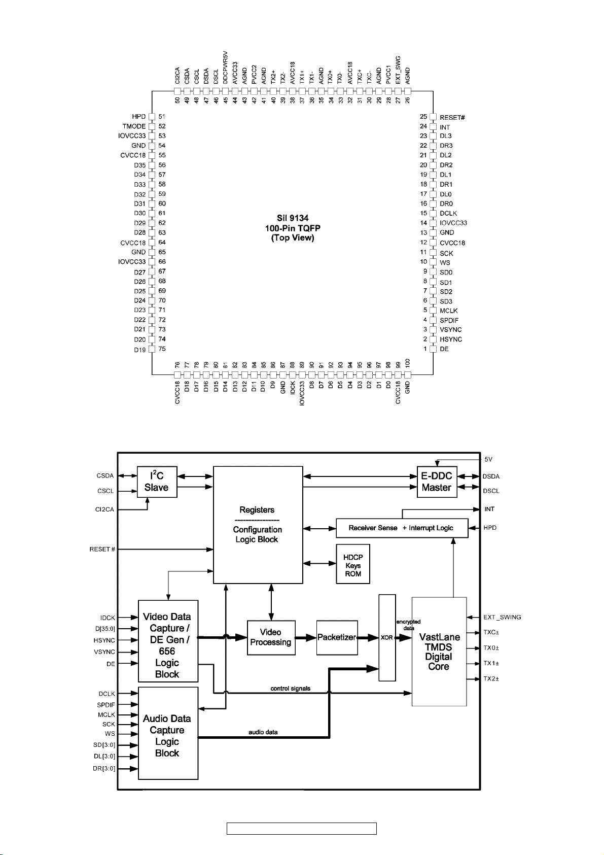
Sil9134 (IC1009)
Functional Block Diagram
57
AVR-1909/789, AVC-1909
Page 58

GLT5640L32 (IC1014)
Block Diagram
58
AVR-1909/789, AVC-1909
Page 59

W9864G2GH (IC1022)
W9864G2GH Block Diagram
59
AVR-1909/789, AVC-1909
Page 60

W9864G2GH-6 Pim Description
60
AVR-1909/789, AVC-1909
Page 61

Sil9185 (IC1002)
AGND
R1XC+
R1XC-
AVCC18
HPD1
I2CSEL/
INT
DGND
DVCC18
RPWR0
DSCL0
DSDA0
AVCC18
R0X2+
R0X2-
AGND
R0X1+
R0X1-
AVCC33
R0X0+
R0X0-
R1X0-
R1X0+
AVCC33
R1X1-
R1X1+
AGND
R1X2-
R1X2+
AVCC18
DSDA1
DSCL1
RPWR1
CEC_D
CEC_A
AVCC33
HPD2
AVCC18
R2XC-
R2XC+
AGND
393837363534333231302928272625
40
41
42
43
44
45
46
47
48
49
50
51
52
53
54
55
56
57
58
59
60
61
64656667686970717273747576
63
62
Sil 9185
80-Pin TQFP
(Top View)
242322
78
77
21
AGND
20
19
R0XC+
R0XC-
18
17
AVCC18
HPD0
16
LSCL/
15
EPSEL[1]
LSDA/
14
EPSEL[0]
13
RESET#
12
EXTSWING
11
TxC-
10
TxC+
9
AGND
8
Tx0-
7
Tx0+
6
AVCC18
5
Tx1-
4
Tx1+
3
AGND
2
Tx2-
1
79
Tx2+
80
Sil9185 Block Diagram
R0X0+/R0X1+/R0X2+/-
R0XC+/-
R1X0+/R1X1+/R1X2+/-
R1XC+/-
R2X0+/R2X1+/R2X2+/-
R2XC+/-
R2X0-
Termination/
Termination/
Termination/
R2X0+
AVCC33
Equalizer
Equalizer
Equalizer
R2X1-
R2X1+
Receiver Block
R2X2-
AGND
R2X2+
AVCC18
EPSEL1/
EPSEL0/
LSDA
LSCL
Config
Logic
Configuration Block
PLL
5V Switch
DSCL2
DSDA2
RPWR2
Port0_DDC
Port1_DDC
2
I C Switch
DPLL
Oversample
HPD
Switch
DGND
RSVDL
DVCC18
Port2_DDC
TX_DDC
HPDIN
TSDA
CEC
TSCL
AGND
TPWR/
I2CADDR
EDID Block
EDID
RAM
Transmitter
Block
Transmit
Drivers
CEC I/F
TX0+/-
TX1+/-
TX2+/-
TXC+/-
HPD0
HPD1
RPWR0
RPWR1
RPWR2
TPWR
HPD2
I2CADDR/
61
AVR-1909/789, AVC-1909
HPDIN
CEC_A
CEC_D
Page 62

LC89057W (IC1027)
36 RERR1RXOUT
35 INT2RX0
34 CKST3RX1
33 AUDIO/VO4RX2
TOP VIEW
32 EMPHA/UO5RX3
31 DGND6DGND
30 DVDD7DVDD
29 XIN8RX4
28 XOUT9RX5/VI
27 XMCK10RX6/UI
26 DVDD11DVDD
25 DGND12DGND
LC89057W Block Diagram
EMPHA/UO33AUDIO/VO35INT40CL39CE38DI
32
Clock
Selector
Microcontroller
I/F
Data
Selector
I/N
1
24 SDIN37DO
23 SLRCK38DI
22 SBCK39CE
21 RDATA40CL
20 RLRCK41XMODE
19 DVDD42DGND
18 DGND43DVDD
17 RBCK44TMCK/PIO0
16 RMCK45TBCK/PIO1
15 AGND46TLRCK/PIO2
14 AVDD47TDATA/PIO3
13 LPF48TXO/PIOEN
RXOUT
RX0
RX1
RX2
RX3
RX4
RX5/VI
RX6/UI
LPF
TMCK/PIO0
TBCK/PIO1
TLRCK/PIO2
TDATA/PIO3
2
3
4
5
8
9
10
13
44
45
46
47
Input
Selector
Modulation
or
Parallel Port
C bit, U bit
Demodulation
&
Lock Detect
PLL
XMODE
41
37
36
21
24
16
17
20
22
23
DO
RERR
RDATA
SDIN
RMCK
RBCK
RLRCK
SBCK
SLRCK
TXO/PIOEN
48
28
29
XOUT
XIN
LC89057W Terminal Function
Pin
No.
1 RXOUT O Input bi-phase select data output terminal
2 RX0 I TTL compatible digital data input terminal
3 RX1 I Coaxial compatible amp built-in digital data input terminal
4 RX2 I TTL compatible digital data input terminal
5 RX3 I TTL compatible digital data input terminal
6 DGND — Digital GND
7 DVDD — Digital power
8 RX4 I TTL compatible digital data input terminal
9 RX5/VI I TTL compatible digital data/Validity flag input terminal for modulation
10 RX6/UI I TTL compatible digital data/User data input terminal for modulation
11 DVDD — Digital power for PLL
12 DGND — Digital GND for PLL
13 LPF O PLL loop filter connecting terminal
14 AVDD — Analog power for PLL
15 AGND — Analog GND for PLL
16 RMCK O RMCK clock output terminal (256fs, 512fs, XIN, VCO)
17 RBCK O/I RBCK clock in/output terminal (64fs)
18 DGND — Digital GND
19 DVDD — Digital power
20 RLRCK O/I RLRCK clock in/output terminal (fs)
21 RDATA O Serial audio data output terminal
22 SBCK O SBCK clock output terminal (32fs, 64fs, 128fs)
23 SLRCK O SLRCK clock output terminal (fs/2, fs, 2fs)
24 SDIN I Serial audio data input ter minal
25 DGND — Digital GND
26 DVDD — Digital power
27 XMCK O Osc. amp output terminal
Pin Name
I/O
Function
27
XMCK34CKST
62
AVR-1909/789, AVC-1909
Page 63

Pin
No.
28 XOUT O X’tal osc. connecting output terminal
29 XIN I X’tal osc. connection, external clock input terminal (24.576MHz or 12.288MHz)
30 DVDD — Digital power
31 DGND — Digital GND
32 EMPHA/UO I/O Emphasis information/U-data output/Chip address setting terminal
33 AUDIO/VO I/O Non-PCM detect/V-flag output/ Chip address setting terminal
34 CKST I/O Clock switch transition period output/Demodulation master or slave function switching terminal
35 INT I/O Interrupt output for μcom (Interrupt factor selectable)/Modulation or general I/O switching terminal
36 RERR O PLL lock error, data error flag output
37 DO O μcom I/F, read out data output terminal (3-state)
38 DI I μcom I/F, write data input terminal
39 CE I μcom I/F, chip enable input terminal
40 CL I μcom I/F, clock input terminal
41 XMODE I System reset input terminal
42 DGND — Digital GND
43 DVDD — Digital power
44 TMCK/PIO0 I/O 256fs system clock input for modulation/General I/O in/output terminal
45 TBCK/PIO1 I/O 64fs bit clock input for modulation/General I/O in/output terminal
46 TLRCK/PIO2 I/O fs clock input for modulation/General I/O in/output terminal
47 TDATA/PIO3 I/O Serial audio data input for modulation/General I/O in/output terminal
48 TXO/PIOEN O/I Modulation data output/ General I/O enable input terminal
* For latch-up countermeasure, perform each power supply ON/OFF in the same timing.
Pin Name I/O
Function
NJW1321 (IC2023)
Block Diagram
63
AVR-1909/789, AVC-1909
Page 64

ADAU1328 (IC1026)
64
AVR-1909/789, AVC-1909
Page 65

ADV7172KSTZ (IC1019)
ADV7172KSTZ Block Diagram
65
AVR-1909/789, AVC-1909
Page 66

ADV7172KSTZ Pin Function Description
66
AVR-1909/789, AVC-1909
Page 67

F2621E-01(IC1037 : for E3 model only)
SAII_DATA
SAII_EN
SAII_CLK
VDD
I2S_OCLK
MUTE
I2S_LRCLK
VSS
I2S_SCLK
VDD
I2S_DATA
VSS
Function Discription
LSDP
VSS
SC_TX_OUT
VDD
SC_RX_IN
RFU (I2C_SCL)
RFU (I2C_SDA)
VDD
ANT_REV
VSS
RESET#
SLAVE_SEL
XMDTIC
VDD
42
43
4847464544
1
2
3
4
5
6
7
8
9
10
11
12
1314151617181920212223
XM/DT IC
Rev 3B/4A
VSS
I2S_RATE
LINKACTIVE
COMM_TX_EN
COMM_RX_P
COMM_RX_M
414039
VSS
VDD
38
37
36
35
34
33
32
31
30
29
28
27
26
25
24
VSS
COMM_TX_P
COMM_TX_M
Inter-IC
Sound
(I2S)
HSDP_EN#
DT4_MODE
HSDP_CLK
VDD
HSDP_DATA
VSS
TEST
SC_RATE
OSC_IN
VDD
OSC_OUT
VSS
I2S_OCLK (M=o, S=n/u)
I2S_LRCLK (M=o; S=i)
I2S_SCLK (M=o; S=i)
I2S_DATA (M=o; S=i)
I2S_RATE (M=o, S=n/u)
MUTE (M=o, S=n/u)
3.3V
GND
COMM_TX_P
COMM_TX_M
COMM_RX_P
COMM_RX_M
LINKACTIVE (M=o, S=o)
COMM_TX_EN (M=o, S=o)
OSC_IN
OSC_OUT
OSC
High Speed
Data Port
(HSDP)
Low Speed
Data Port
(LSDP)
RAM
COMM ENGINE
SAII
Sys Ctrlr
(CBM)
Bus I/F
Misc Status
& Control
COMM I/F
HSDP_EN# (M=o; S=i)
HSDP_CLK (M=o; S=i)
HSDP_DATA (M=o; S=i)
LSDP (M=o; S=i)
SAII_REQ (M=i; S=o)
SAII_CLK (M=o; S=i)
SAII_DATA (M=o; S=i)
SC_RX_IN (M=i, S=i)
SC_TX_OUT (M=o, S=o)
SC_RATE (M=i, S=o)
RESET# (M=i, S=i)
ANT_REV (M=o, S=n/u)
DT4_MODE (M=i, S=i)
SLAVE_SEL (M=i, S=i)
TEST (M=i, S=i)
(RFU – I2C_SCL)
(RFU – I2C_SDA)
67
AVR-1909/789, AVC-1909
Page 68

p
Pin
#
1 LSDP
3 SC_TX_OUT
5 SC_RX_IN
6 RFU (I2C-SCL)
7 RFU (I2C-SDA)
9 ANT_REV
11 RESET#
12 SLAVE_SEL
13 I2S_RATE
14 LINKACTIVE
15 COMM_TX_EN
18 COMM_RX_P
19 COMM_RX_M
22 COMM_TX_M
23 COMM_TX_P
26 OSC_OUT
28 OSC_IN
29
Pin Name
SC_RATE
(Rev 4A only, pull
down for rev 3B)
Direct-
ion
S=In
M=Out
S=Out
M=Out
S=In
M=In
S=In
M=In
S=In
M=In
S=n/u
M=Out
S=In
M=In
S=In
M=In
S=Out
M=Out
S=Out
M=Out
S=Out
M=Out
S=In
M=In
S=In
M=In
S=Out
M=Out
S=Out
M=Out
S=Out
M=Out
S=In
M=In
S=Out
M=In
Function
in Slave Mode
Low Speed Data Port Input Low Speed Data Port Output
System Controller Bus (CBM)
Transmit Data Out
System Controller Bus (CBM)
Receive Data In
Reserved for Future Use (pull
down with a 100k resistor to
Ground)
Reserved for Future Use (pull
down with a 100k resistor to
Ground)
Not used in Slave mode, leave
unconnected
Asynchronous Reset In,
(Active Low)
Master/Slave Mode Select In
(High = Slave Mode)
Output driven high, leave
unconnected
Link Active indicator (High =
DT bus link is active and data
is flowing)
DT Comm Bus External
Transceiver Direction
Control Output (0=Tx, 1=Rx)
DT Differential Comm Bus
Internal Receiver Positive In
DT Differential Comm Bus
Internal Receiver Negative In
DT Differential Comm Bus
Internal Transmitter Negative
Out
DT Differential Comm Bus
Internal Transmitter Positive
Out
Crystal Driver Output Crystal Driver Output
Crystal/ Ext. Clock Input Crystal/ Ext. Clock Input
SC interface baud rate Output
(High = DT4_MODE is high
and the Master DTIC is
operating at 115.2K baud)
System Controller Bus (CBM)
Transmit Data Out
System Controller Bus (CBM)
Receive Data In
Reserved for Future Use (pull
down with a 100k resistor to
Ground)
Reserved for Future Use (pull
down with a 100k resistor to
Ground)
Indication of incompatible
antenna (
4.3.2 for usage)
Asynchronous Reset In,
(Active Low)
Master/Slave Mode Select In
(Low = Master Mode)
Indicator of incoming I2S data
rate (see section 4.4.2)
Link Active indicator (High =
DT bus link is active and data
is flowing)
DT Comm Bus External
Transceiver Direction
Control Output (0=Tx, 1=Rx)
DT Differential Comm Bus
Internal Receiver Positive In
DT Differential Comm Bus
Internal Receiver Negative In
DT Differential Comm Bus
Internal Transmitter Negative
Out
DT Differential Comm Bus
Internal Transmitter Positive
Out
SC interface baud rate select
Input
(High = 115.2K baud, Low =
9600 baud)
Function
in Master Mode
refer to section
Notes
Out= 4mA, SLC
In=LVTTL S/T
4mA, SLC
LVTTL S/T
LVTTL S/T
LVTTL S/T
4mA, SLC
LVTTL S/T
LVTTL S/T
4mA, SLC
4mA, SLC
4mA, SLC
LVDS in+
LVDS in–
LVDS out–
LVDS out+
Out= 4mA, SLC
In=LVTTL S/T
30 TEST
S=In
M=In
Factory Test Mode Select
(1=Test, 0= Normal Oper.)
68
AVR-1909/789, AVC-1909
Factory Test Mode Select
(1=Test, 0= Normal Oper.)
LVTTL S/T
Page 69

Pin
#
32 HSDP_DATA
34 HSDP_CLK
35 DT4_MODE
36 HSDP_EN#
37 I2S_DATA
39 I2S_SCLK
41 I2S_LRCLK
43 I2S_OCLK
44 MUTE
45 SAII_CLK
47 SAII_DATA
48 SAII_REQ
Pin Name
Direct-
ion
S=In
M=Out
S=In
M=Out
S=In
M=In
S=In
M=Out
S=In
M=Out
S=In
M=Out
S=In
M=Out
S=In
M=Out
S=n/u
M=Out
S=Out
M=In
S=Out
M=In
S=In
M=Out
Function
in Slave Mode
High Speed Data Port Data
Input
High Speed Data Port Clock
Input
Enables/Disables driver on
SC_RATE and ANT_REV
(High = enable driver) This
pin was VSS on rev 3
XM/DT IC
High Speed Data Port Enable
Input (Active low)
I2S Digital Audio Port Data In
I2S Digital Audio Port Bit
Clock In
I2S Digital Audio Port
Left/Right Clock In
I2S Digital Audio Port
Oversample Clock
(not used, leave unconnected)
Not used in Slave mode, leave
unconnected
SAII Port Clock Output SAII Port Clock Input
SAII Port Data Output SAII Port Data Input
SAII Port Request Input SAII Port Request Output
High Speed Data Port Data
Output
High Speed Data Port Clock
Output
Enables/Disables drivers on
MUTE and ANT_REV (High
= enable drivers) This pin
was VSS on rev 3 XM/DT IC
High Speed Data Port Enable
Output (Active low)
I2S Digital Audio Port Data
Out
I2S Digital Audio Port Bit
Clock Out
I2S Digital Audio Port
Left/Right Clock Out
I2S Digital Audio Port
Oversample Clock Out
Provides a mechanism for
muting the audio during an
I2S rate change (High=mute)
Function
in Master Mode
Notes
Out= 4mA, SLC
In=LVTTL S/T
Out= 4mA, SLC
In=LVTTL S/T
In=LVTTL S/T
Out= 4mA, SLC
In=LVTTL S/T
Out= 4mA, SLC
In=LVTTL S/T
Out= 4mA, SLC
In=LVTTL S/T
Out= 4mA, SLC
In=LVTTL S/T
Out= 4mA, SLC
Out= 4mA, SLC
Out= 4mA, SLC
In=LVTTL S/T
Out= 4mA, SLC
In=LVTTL S/T
Out= 4mA, SLC
In=LVTTL S/T
69
AVR-1909/789, AVC-1909
Page 70

EN29LV160AB-70TI (IC1023)
A15
A14
A13
A12
A11
A10
A9
A8
A19
NC
WE#
RESET#
NC
NC
RY/BY#
A18
A17
A7
A6
A5
A4
A3
A2
A1
Block Diagram
Vcc
Vss
WE#
Control
State
1
2
3
4
5
6
7
8
9
10
11
12
13
14
15
16
17
18
19
20
21
22
23
24
RY/BY#
Standa rd
TSOP
Block Protect Switches
Erase VoltageGenerator
48
47
46
45
44
43
42
41
40
39
38
37
36
35
34
33
32
31
30
29
28
27
26
25
A16
BYTE#
Vss
DQ15/A-1
DQ7
DQ14
DQ6
DQ13
DQ5
DQ12
DQ4
Vcc
DQ11
DQ3
DQ10
DQ2
DQ9
DQ1
DQ8
DQ0
OE#
Vss
CE#
A0
DQ0-DQ15 (A-1)
Input/OutputBuffers
CE#
OE#
A0-A19
Command
Register
Program Voltage
Generator
TimerVcc Detector
STB
Chip Enable
Output Enable
Logic
Y-Decoder
Address Latc h
X-Decoder
STB
Data Latch
Y-Gati ng
Cell Matrix
70
AVR-1909/789, AVC-1909
Page 71

LA73053 (IC2016)
71
AVR-1909/789, AVC-1909
Page 72

EPM3032A-TC44 (IC1029)
I/O
I/O
I/O
VCC
INPUT/OE2/GCLK2
INPUT/GCLRn
Pin 1
INPUT/OE1
INPUT/GCLK1
GND
I/O
I/O
Pin 34
I/O/TDI
I/O
I/O
GND
I/O
I/O
I/O/TMS
I/O
VCC
I/O
GND
I/O
Pin 12 Pin 23
BH7868 (IC1080)
EPM3032A
EPM3064A
I/O
I/O
I/O
GND
VCC
I/O
I/O/TDO
I/O
GND
VCC
I/O
I/O
I/O/TCK
I/O
GND
I/O
I/O
I/O
I/O
I/O
I/O
72
AVR-1909/789, AVC-1909
Page 73

LC72722 (IC801 : for E2 model only)
Block Diagram
+5V +5V
Vdda
Vssa
MPXIN
REFERENCE
VOLTAGE
ANTIALIASING
FILTER
V
REF
57 kHz
BPF
(SCF)
REF
124V
SYR
223MPXIN CE
322Vdda DI
421Vssa CL
520FLOUT DO
LC72722
619CIN
LC72722M
718T1 SYNC
LC72722PM
RDS-ID
817T2 T7(CORREC/ARI-ID/TA/BEO)
916T3(RDCL) T6(ERROR/57K/TP/BE1)
10 15T4(RDDA) Vssd
11 14T5(RSFT) Vddd
OUT
12 13X
X
IN
Top view
CINFLOUT
V
SMOOTHING
FILTER
+
Ð
REF
PLL
(57 kHz)
CLOCK
RECOVERY
(1187.5 Hz)
DATA
DECODER
Vddd
Vssd
RDS-ID
DO
CL
CE
T1
T2
T3 to T7
DI
CCB
TEST
RAM
(24 BLOCK DATA)
MEMORY CONTROL
ERROR CORRECTION
(SOFT DECISION)
CLK(4.332 MHz)
OSC/DIVIDER
X
IN
X
OUT
SYNC/EC CONTROLLER
SYNC
DETECT-1
SYNC
DETECT-2
LC74782 (IC2017) SN74LVC244APW (IC1028)
SYNC
SYR
73
AVR-1909/789, AVC-1909
Page 74

BU4094BCF (IC110,111,2019 : for AVR-1910)
Y0
1
Y2
2
COMMON
Y
3
Y3
4
Y1
5
INH
6
VEE
7
VSS
8
16
15
14
13
12
11
10
9
VDD
X2
X1
X
X
0
X3
A
B
Y
0
B
Y
OUT / IN
INH
V
EE
X
OUT / IN
A
COMMON
Y
2
Y3
Y1
X2
X1
X0
X3
(IC110,111,2019,2020 : for AVC-1910) BU4052 (IC2026, 2027 : AVC model)
ROBE
ERIAL
IN
LOCK
V
1
2
3
4
1
Q
5
Q2
6
Q3
7
Q4
8
SS
16
15
14
13
12
11
10
9
V
DD
OUTPUT
ENABLE
Q5
Q6
Q7
Q8
Q'S
QS
TC4051 (IC2002, 2003, 2004,
2009, 2010, 2011) TC4052 (IC2014, 2015) TC4053 (IC2006)
MM74HC4053 (IC2007)
74
AVR-1909/789, AVC-1909
Page 75

2. FL DISPLAY
FLD (HCA-19MM02T) (FLT301)
PIN CONNECTION
GRID ASSIGNMENT
75
AVR-1909/789, AVC-1909
Page 76

ANODE CONNECTION
76
AVR-1909/789, AVC-1909
Page 77

PRINTED WIRING BOARDS
MAIN P.W.B. UNIT(1/2)
77
AVR-1909/789, AVC-1909
COMPONENT SIDE
Page 78

MAIN P.W.B. UNIT(2/2)
78
AVR-1909/789, AVC-1909
FOIL SIDE
Page 79

FRONT P.W.B. UNIT (1/2)
79
AVR-1909/789, AVC-1909
COMPONENT SIDE
Page 80

FRONT P.W.B. UNIT (2/2)
80
AVR-1909/789, AVC-1909
FOIL SIDE
Page 81

INPUT P.W.B. UNIT
COMPONENT SIDE
AVR-1909/789, AVC-1909
FOIL SIDE
81
Page 82

POWER P.W.B. UNIT (1/2)
DENON
DENON
COMPONENT SIDE
82
AVR-1909/789, AVC-1909
Page 83

POWER P.W.B. UNIT (2/2)
83
AVR-1909/789, AVC-1909
FOIL SIDE
Page 84

CPU P.W.B. UNIT
COMPONENT SIDE
84
AVR-1909/789, AVC-1909
FOIL SIDE
Page 85

HDMI P.W.B. UNIT
COMPONENT SIDE
AVR-1909/789, AVC-1909
FOIL SIDE
85
Page 86

VIDEO P.W.B. UNIT (1/2)
DENON
COMPONENT SIDE
86
AVR-1909/789, AVC-1909
Page 87
VIDEO P.W.B. UNIT (2/2)
87
AVR-1909/789, AVC-1909
FOIL SIDE
Page 88

2CH P.W.B. UNIT
COMPONENT SIDE
88
AVR-1909/789, AVC-1909
FOIL SIDE
Page 89

SIRIUS P.W.B. UNIT POWER REG P.W.B. UNIT
DENON
DENON
COMPONENT SIDE
COMPONENT SIDE
FOIL SIDE
89
AVR-1909/789, AVC-1909
Page 90

---MEMO---
90
AVR-1909/789, AVC-1909
Page 91

NOTE FOR PARTS LIST
• Parts for which "nsp" is indicated on this table cannot be supplied.
• When ordering of part, clearly indicate "1" and "I" (i) to avoid mis-
supplying.
• Ordering part without stating its part number can not be supplied.
• Part indicated with the mark " ★ " is not illustrated in the exploded view.
• Not including General-purpose Carbon Film Resistor in the P.W.Board
parts list. (Refer to the Schematic Diagram for those parts.)
• Not including General-purpose Carbon Chip Resistor in the P.W.Board
parts list. (Refer to the Schematic Diagram for those parts.)
WARNING:
Parts marked with this symbol z have critical characteristics.
Use ONLY replacement parts recommended by the manufacturer.
ll
Resistors
l
ll
Ex.: RN 14K 2E 182 G FR
Type Shape Power Resist- Allowable Others
and per- ance error
formance
部品表について
1.部品表に "nsp" と記載されている部品は供給できません。
2.部品を発注する際は特に数字の " 1 " と英字の "I" との区別をはっ
きり記入してください。
3.部品番号を表示していない部品は供給できません。
4.z 印の部品は安全上重要な部品です。交換するときは、安全およ
び性能維持のため必ず指定の部品をご使用ください。
5.★印のついている部品は分解図中には記載していません。
6.汎用カーボン抵抗器は記載していません。定数は回路図を参照願い
ます。
7.汎用カーボンチップ抵抗器は記載していません。定数は回路図を参
照願います。
8.部品表の抵抗器、コンデンサの品名記号の読み方は表を参照してく
ださい。
RN 14K 2E 182 G FR
RD : Carbon 2B : 1/8W F : ±1% P : Pulse-resistant type
RC : Composition 2E : 1/4W G : ±2% NL : Low noise type
RS : Metal oxide film 2H : 1/2W J : ±5% NB : Non-burning type
RW : Winding 3A : 1W K : ±10% FR : Fuse-resistor
RN : Metal film 3D : 2W M : ±20% F : Lead wire forming
RK : Metal mixture 3F : 3W
] Resistance
1 8 2 ⇒ 1800 ohm = 1.8 kohm
s
s
• Units: ohm
1 R 2 ⇒ 1.2 ohm
s
s
• Units: ohm
ll
Capacitors
l
ll
Ex.: CE 04W 1H 2R2 M BP
Type Shape Dielectric Capacity Allowable Others
3H : 5W
Indicates number of zeros after effective number.
2-digit effective number.
1-digit effective number.
2-digit effective number, decimal point indicated by R.
and per- strength error
formance
CE : Aluminum foil 0J : 6.3V F : ±1% HS : High stability type
electrolytic
CA : Aluminum solid 1A : 10V G : ±2% BP : Non-polar type
electrolytic
CS : Tantalum electrolytic 1C : 16V J : ±5% HR : Ripple-resistant type
CQ : Film 1E : 25V K : ±10% DL : For change and discharge
CK : Ceramic 1V : 35V M : ±20% HF : For assuring high
CC : Ceramic 1H : 50V Z : +80% U : UL part
CP : Oil 2A : 100V –20% C : CSA part
CM : Mica 2B : 125V P : +100% W : UL-CSA type
CF : Metallized 2C : 160V –0% F : Lead wire for ming
CH : Metallized 2D : 200V C : ±0.25pF
2E : 250V D : ±0.5pF
2H : 500V = : Others
2J : 630V
requency
RD : 2B : 1/8 W F : ±1% P :
RC : 2E : 1/4 W G : ±2% NL :
RS : 2H : 1/2 W J : ±5% NB :
RW : 3A : 1 W K : ±10% FR :
RN : 3D : 2 W M : ±20% F :
RK : 3F : 3 W
∗
CE 04W 1H 2R2 M BP
CE : 0J : 6.3 V F : ±1% HS :
CA : 1A : 10 V G : ±2% BP :
CS : 1C : 16 V J : ±5% HR :
CQ : 1E : 25 V K : ±10% DL :
CK : 1V : 35 V M : ±20% HF :
CC : 1H : 50 V Z : +80% U : UL
CP : 2A : 100 V −20% C : CSA
CM : 2B : 125 V P : +100% W : UL-CSA
CF : 2C : 160 V − 0% F :
CH : 2D : 200 V C : ±0.25pF
3H : 5 W
18 2
1R 2
Ö
2
Ö
1
2 R
2E : 250 V D : ±0.5pF
2H : 500 V = :
2J : 630 V
1800
1.2
=1.8k
0
] Capacity (electrolyte only)
2 2 2 ⇒ 2200μF
s
s
• Units: μF.
2 R 2 ⇒ 2.2μF
s
s
• Units: μF.
] Capacity (except electrolyte)
2 2 2 ⇒ 2200pF=0.0022μF
s
s
• Units: pF.
2 2 1 ⇒ 220pF
s
s
• Units: pF.
• When the dielectric strength is indicated in AC, "AC" is included after the dieelectric
strength value.
Indicates number of zeros after effective number.
2-digit effective number.
1-digit effective number.
2-digit effective number, decimal point indicated by R.
(More than 2) Indicates number of zeros after effective number.
(0 or 1) Indicates number of zeros after effective number.
2-digit effective number.
2-digit effective number.
AVR-1909/789, AVC-1909
91
∗
22 2
22 2
2200μF
Ö
2
μ
F
2200pF=0.0022μF
Ö
(0 2 )
2
p
F
0
0
2R 2
22 1
Ö
1
2 R
μ
F
Ö
(0 0 1 )
2
p
F
AC
2.2μF
220pF
0
Page 92

PARTS LIST OF P.W.B. UNIT
*本表に"nsp" と記載されている部品は供給できません。
* Parts for which "nsp" is indicated on this table cannot be supplied.
*本表に"nsp" と記載されている基板 ASS'Y は供給できません。基板 ASS'Y の修理の際には基板部品表を確認のうえ、交換部品を発注してください。
*
P.W.B. ASS'Y for which "nsp" is indicated on this table cannot be supplied. When repairing the P.W.B. ASS'Y, check the board parts table and order replacement parts.
*本表に記載されている部品は、補修用部品のため製品に使用している部品とは一部、形状、寸法などが異なる場合があります。
* The parts listed below are for maintenance only, might differ from the parts used in the unit in appearances or dimensions.
Note: The symbols in the column "Remarks" indicate the following destinations.
E3 : U.S.A. & Canada model E2 : Europe model EA : Australia model
E1C : China model AVC1909 : Japan model
MAIN P.W.B. UNIT ASS'Y
Ref. No. Part No. Part Name Remarks Q'ty New
SEMICONDUCTORS GROUP
IC100 963239001880S IC AZ4580M JP
IC110,111 00D9630218807 IC BU4094BCF-E2
IC231 00D9600174104 IC CXA1511M-T4
J121458000020S
J040140940030S
J030151100010S
Q101 00D9600196302 TR KTA1268BL
Q102 00D9600196700 TR KTC3200BL
Q104 00D9600196700 TR KTC3200BL
Q104C 00D9600196700 TR KTC3200BL
Q104FL 00D9600196700 TR KTC3200BL
Q104FR 00D9600196700 TR KTC3200BL
Q104SL 00D9600196700 TR KTC3200BL
Q104SR 00D9600196700 TR KTC3200BL
Q105,106 00D9600196700 TR KTC3200BL
Q106C 00D9600196205 TR KSA992F
Q106FL 00D9600196205 TR KSA992F
Q106FR 00D9600196205 TR KSA992F
Q106SL 00D9600196205 TR KSA992F
Q106SR 00D9600196205 TR KSA992F
Q107C 00D9600196205 TR KSA992F
Q107FL 00D9600196205 TR KSA992F
Q107FR 00D9600196205 TR KSA992F
Q107SL 00D9600196205 TR KSA992F
Q107SR 00D9600196205 TR KSA992F
Q108 00D9600196700 TR KTC3200BL
Q108C 00D9600196700 TR KTC3200BL
Q108FL 00D9600196700 TR KTC3200BL
Q108FR 00D9600196700 TR KTC3200BL
Q108SL 00D9600196700 TR KTC3200BL
Q108SR 00D9600196700 TR KTC3200BL
Q109,110 00D9600196700 TR KTC3200BL
Q111 00D9600196302 TR KTA1268BL
Q112 00D9630121509 TR KTC3875S
Q128 00D9600097207 TR KRA102M
Q130 00D9600196302 TR KTA1268BL
Q131,132 00D9630219602 TR KRC106M
Q133-138 00D9600097207 TR KRA102M
Q141SW 00D9630044301 TR KTC2875B(MB)
Q142 00D9600196700 TR KTC3200BL
Q142SW 00D9630044301 TR KTC2875B(MB)
Q143,144 00D9600196302 TR KTA1268BL
Q145 00D9600196700 TR KTC3200BL
Q146,147 00D9600196302 TR KTA1268BL
Q151 00D9600196302 TR KTA1268BL
Q156 00D9600097304 TR KRC102M
J5001268B0050S
J5023200B0050S
J5023200B0050S
J5023200B0050S
J5023200B0050S
J5023200B0050S
J5023200B0050S
J5023200B0050S
J5023200B0050S
J5000992F0050S
J5000992F0050S
J5000992F0050S
J5000992F0050S
J5000992F0050S
J5000992F0050S
J5000992F0050S
J5000992F0050S
J5000992F0050S
J5000992F0050S
J5023200B0050S
J5023200B0050S
J5023200B0050S
J5023200B0050S
J5023200B0050S
J5023200B0050S
J5023200B0050S
J5001268B0050S
J522038750210S
J6002202M0010S
J5001268B0050S
J6020106M0010S
J6002202M0010S
J5222875B0010S
J5023200B0050S
J5222875B0010S
J5001268B0050S
J5023200B0050S
J5001268B0050S
J5001268B0050S
J6020102M0010S
92
AVR-1909/789, AVC-1909
Page 93

Ref. No. Part No. Part Name Remarks Q'ty New
Q165 00D9600196700 TR KTC3200BL
Q166-170 00D9600196302 TR KTA1268BL
Q221L 00D9630044301 TR KTC2875B(MB)
Q221R 00D9630044301 TR KTC2875B(MB)
Q227L 00D9630044301 TR KTC2875B(MB)
Q227R 00D9630044301 TR KTC2875B(MB)
Q231 00D9600097003 TR KRA104M
Q541 00D9630121208 TR KRC107M
J5023200B0050S
J5001268B0050S
J5222875B0010S
J5222875B0010S
J5222875B0010S
J5222875B0010S
J6000104M0010S
J6020107M0010S
D101C 00D9630355401 D,SWITCHING KDS4148U
D101FL 00D9630355401 D,SWITCHING KDS4148U
D101FR 00D9630355401 D,SWITCHING KDS4148U
D101SL 00D9630355401 D,SWITCHING KDS4148U
D101SR 00D9630355401 D,SWITCHING KDS4148U
D102C 00D9630355401 D,SWITCHING KDS4148U
D102FL 00D9630355401 D,SWITCHING KDS4148U
D102FR 00D9630355401 D,SWITCHING KDS4148U
D102SL 00D9630355401 D,SWITCHING KDS4148U
D102SR 00D9630355401 D,SWITCHING KDS4148U
D105C 00D9630020309 D,SWITCHING 1SS133T
D105FL 00D9630020309 D,SWITCHING 1SS133T
D105FR 00D9630020309 D,SWITCHING 1SS133T
D105SL 00D9630020309 D,SWITCHING 1SS133T
D105SR 00D9630020309 D,SWITCHING 1SS133T
D106 00D9630355401 D,SWITCHING KDS4148U
D106C 00D9630020309 D,SWITCHING 1SS133T
D106FL 00D9630020309 D,SWITCHING 1SS133T
D106FR 00D9630020309 D,SWITCHING 1SS133T
D106SL 00D9630020309 D,SWITCHING 1SS133T
D106SR 00D9630020309 D,SWITCHING 1SS133T
D107 00D9630355401 D,SWITCHING KDS4148U
D114,115 00D2760338007 D,RECTIFIER BRIDGE
S4VB20-5001L20
D114,115 00D9600197107 D,RECTIFIER BRIDGE KBPC604 E3
D139 00D9630020309 D,SWITCHING 1SS133T
D140,141 00D9630328409 D,SWITCHING 1N4007
D142 00D9630355401 D,SWITCHING KDS4148U
D143-152 00D9630020309 D,SWITCHING 1SS133T
D153 00D9630355401 D,SWITCHING KDS4148U
D154-157 00D9630020309 D,SWITCHING 1SS133T
D231 00D9630355401 D,SWITCHING KDS4148U
D541 00D9630355401 D,SWITCHING KDS4148U
E2, EA, JP
K005041480030S
K005041480030S
K005041480030S
K005041480030S
K005041480030S
K005041480030S
K005041480030S
K005041480030S
K005041480030S
K005041480030S
K000013300520S
K000013300520S
K000013300520S
K000013300520S
K000013300520S
K005041480030S
K000013300520S
K000013300520S
K000013300520S
K000013300520S
K000013300520S
K005041480030S
K047400400020S
K047604000020S
K000013300520S
K000400700010S
K005041480030S
K000013300520S
K005041480030S
K000013300520S
K005041480030S
K005041480030S
ZD101 00D9630058601 D,ZENER MTZJ12B
ZD101C 00D9630367008 D,ZENER 0.2W 3.3V UDZ
ZD101FL 00D9630367008 D,ZENER 0.2W 3.3V UDZ
ZD101FR 00D9630367008 D,ZENER 0.2W 3.3V UDZ
ZD101SL 00D9630367008 D,ZENER 0.2W 3.3V UDZ
ZD101SR 00D9630367008 D,ZENER 0.2W 3.3V UDZ
ZD102C 00D9630382209 D,ZENER 0.2W 3.0V UDZ
ZD102FL 00D9630382209 D,ZENER 0.2W 3.0V UDZ
ZD102FR 00D9630382209 D,ZENER 0.2W 3.0V UDZ
ZD102SL 00D9630382209 D,ZENER 0.2W 3.0V UDZ
ZD102SR 00D9630382209 D,ZENER 0.2W 3.0V UDZ
ZD105 00D9600095500 D,ZENER MTZJ5.1B
ZD231 00D9600095704 D,ZENER MTZJ6.2B
AVR-1909/789, AVC-1909
93
K06012R044520S
K06603R34P400S
K06603R34P400S
K06603R34P400S
K06603R34P400S
K06603R34P400S
K06603R04P400S
K06603R04P400S
K06603R04P400S
K06603R04P400S
K06603R04P400S
K06005R144520S
K06006R244520S
s
s
s
s
s
Page 94

Ref. No. Part No. Part Name Remarks Q'ty New
RESISTORS GROUP
R101 00D9630337801 R,METAL FILM 100-J,2W E3
R103 00D9639005639 R,METAL FILM 100-J,1W
R104 00D9630215907 R,METAL FILM 4.7-J,1W
R104C 00D9639006285 R,FIXED 1WJ-5.6K
R104FL 00D9639006285 R,FIXED 1WJ-5.6K
R104FR 00D9639006285 R,FIXED 1WJ-5.6K
R104SL 00D9639006285 R,FIXED 1WJ-5.6K
R104SR 00D9639006285 R,FIXED 1WJ-5.6K
R105 00D9630232906 R,METAL FILM 47K-F,1/4W
R105C 00D9639006285 R,FIXED 1WJ-5.6K
R105FL 00D9639006285 R,FIXED 1WJ-5.6K
R105FR 00D9639006285 R,FIXED 1WJ-5.6K
R105SL 00D9639006285 R,FIXED 1WJ-5.6K
R105SR 00D9639006285 R,FIXED 1WJ-5.6K
R106C 00D9630215907 R,METAL FILM 4.7-J,1W
R106FL 00D9630215907 R,METAL FILM 4.7-J,1W
R106FR 00D9630215907 R,METAL FILM 4.7-J,1W
R106SL 00D9630215907 R,METAL FILM 4.7-J,1W
R106SR 00D9630215907 R,METAL FILM 4.7-J,1W
R107C 00D9630215907 R,METAL FILM 4.7-J,1W
R107FL 00D9630215907 R,METAL FILM 4.7-J,1W
R107FR 00D9630215907 R,METAL FILM 4.7-J,1W
R107SL 00D9630215907 R,METAL FILM 4.7-J,1W
R107SR 00D9630215907 R,METAL FILM 4.7-J,1W
R108C 00D9630345903 R,FIXED 2WJ-0.47
R108FL 00D9630345903 R,FIXED 2WJ-0.47
R108FR 00D9630345903 R,FIXED 2WJ-0.47
R108SL 00D9630345903 R,FIXED 2WJ-0.47
R108SR 00D9630345903 R,FIXED 2WJ-0.47
R109C 00D9630345903 R,FIXED 2WJ-0.47
R109FL 00D9630345903 R,FIXED 2WJ-0.47
R109FR 00D9630345903 R,FIXED 2WJ-0.47
R109SL 00D9630345903 R,FIXED 2WJ-0.47
R109SR 00D9630345903 R,FIXED 2WJ-0.47
R110C 00D9630345903 R,FIXED 2WJ-0.47
R110FL 00D9630345903 R,FIXED 2WJ-0.47
R110FR 00D9630345903 R,FIXED 2WJ-0.47
R110SL 00D9630345903 R,FIXED 2WJ-0.47
R110SR 00D9630345903 R,FIXED 2WJ-0.47
R111C 00D9630345903 R,FIXED 2WJ-0.47
R111FL 00D9630345903 R,FIXED 2WJ-0.47
R111FR 00D9630345903 R,FIXED 2WJ-0.47
R111SL 00D9630345903 R,FIXED 2WJ-0.47
R111SR 00D9630345903 R,FIXED 2WJ-0.47
R117,118 00D9630144502 R,CEMENT 0.1-J 5W
R118C 00D9639006256 R,FIXED 1WJ-10
R118FL 00D9639006256 R,FIXED 1WJ-10
R118FR 00D9639006256 R,FIXED 1WJ-10
R118SL 00D9639006256 R,FIXED 1WJ-10
R118SR 00D9639006256 R,FIXED 1WJ-10
R119C 00D9639006256 R,FIXED 1WJ-10
R119FL 00D9639006256 R,FIXED 1WJ-10
R119FR 00D9639006256 R,FIXED 1WJ-10
R119SL 00D9639006256 R,FIXED 1WJ-10
R119SR 00D9639006256 R,FIXED 1WJ-10
C060010166520S
C060010165060S
C0604R7065050S
N113135656220S
N113135656220S
N113135656220S
N113135656220S
N113135656220S
C060047343530S
N113135656220S
N113135656220S
N113135656220S
N113135656220S
N113135656220S
C0604R7065050S
C0604R7065050S
C0604R7065050S
C0604R7065050S
C0604R7065050S
C0604R7065050S
C0604R7065050S
C0604R7065050S
C0604R7065050S
C0604R7065050S
N113136647820S
N113136647820S
N113136647820S
N113136647820S
N113136647820S
N113136647820S
N113136647820S
N113136647820S
N113136647820S
N113136647820S
N113136647820S
N113136647820S
N113136647820S
N113136647820S
N113136647820S
N113136647820S
N113136647820S
N113136647820S
N113136647820S
N113136647820S
C141R10069000S
N113135610020S
N113135610020S
N113135610020S
N113135610020S
N113135610020S
N113135610020S
N113135610020S
N113135610020S
N113135610020S
N113135610020S
94
AVR-1909/789, AVC-1909
Page 95

Ref. No. Part No. Part Name Remarks Q'ty New
R127C 00D9639005642 R,METAL FILM 1.2K-J,1W
R127FL 00D9639005642 R,METAL FILM 1.2K-J,1W
R127FR 00D9639005642 R,METAL FILM 1.2K-J,1W
R127SL 00D9639005642 R,METAL FILM 1.2K-J,1W
R127SR 00D9639005642 R,METAL FILM 1.2K-J,1W
R132C 00D9609010719 R,METAL FILM 47-J,1W
R132FL 00D9609010719 R,METAL FILM 47-J,1W
R132FR 00D9609010719 R,METAL FILM 47-J,1W
R132SL 00D9609010719 R,METAL FILM 47-J,1W
R132SR 00D9609010719 R,METAL FILM 47-J,1W
R147-149 00D9630310404 R,METAL FILM 2.2K-J,1W
R160 00D9630310404 R,METAL FILM 2.2K-J,1W
R164 00D9630310404 R,METAL FILM 2.2K-J,1W
R166 00D9630310404 R,METAL FILM 2.2K-J,1W
C060012265050S
C060012265050S
C060012265050S
C060012265050S
C060012265050S
C060047065060S
C060047065060S
C060047065060S
C060047065060S
C060047065060S
C060022265050S
C060022265050S
C060022265050S
C060022265050S
VR101C 00D9600221109
VR101FL 00D9600221109
VR101FR 00D9600221109
VR101SL 00D9600221109
VR101SR 00D9600221109
CAPACITORS GROUP
C101 00D2544580712 C,ELECT 100UF-M/50V E2, EA, JP
C101 00D9639005804 C,ELECT 100UF-M/25V E3
C101C 00D9630234205 C,ELECT 10UF-M/50V E2, EA, JP
C101C 00D9630234506 C,ELECT 47UF-M/50V (Pb Free) E3
C101FL 00D2544583942 C,ELECT 10UF-M/50V E2, EA, JP
C101FL 00D9630234506 C,ELECT 47UF-M/50V (Pb Free) E3
C101FR 00D2544583942 C,ELECT 10UF-M/50V E2, EA, JP
C101FR 00D9630234506 C,ELECT 47UF-M/50V (Pb Free) E3
C101SL 00D9630234205 C,ELECT 10UF-M/50V E2, EA, JP
C101SL 00D9630234506 C,ELECT 47UF-M/50V (Pb Free) E3
C101SR 00D9630234205 C,ELECT 10UF-M/50V E2, EA, JP
C101SR 00D9630234506 C,ELECT 47UF-M/50V (Pb Free) E3
C102 00D9630234506 C,ELECT 47UF-M/50V (Pb Free)
C102C 00D9630234205 C,ELECT 10UF-M/50V
C102FL 00D9609009937 C,ELECT 100UF-M/50V E2, EA, JP
C102FL 00D9609010133 C,ELECT 220UF-M/35V E3
C102FR 00D9609009937 C,ELECT 100UF-M/50V E2, EA, JP
C102FR 00D9609010133 C,ELECT 220UF-M/35V E3
C102SL 00D9630234205 C,ELECT 10UF-M/50V
C102SR 00D9630234205 C,ELECT 10UF-M/50V
C104,105 00D9639006557 C,ELECT 220UF-M/6.3V
C106 00D9630293709 C,ELECT 100UF-M/10V
C107 nsp C,CERAMIC 0.01UF-K/50V
C107C nsp C,FILM 0.1UF-J/50V
C107FL nsp C,FILM 0.1UF-J/50V
C107FR nsp C,FILM 0.1UF-J/50V
C107SL nsp C,FILM 0.1UF-J/50V
C107SR nsp C,FILM 0.1UF-J/50V
C108,109 00D2546276008 C,ELECT 12000UF-M/71V(VSSN)
C109C 00D9630234205 C,ELECT 10UF-M/50V
C109FL 00D2544583942 C,ELECT 10UF-M/50V E2, EA, JP
C109FL 00D9630234205 C,ELECT 10UF-M/50V E3
C109FR 00D2544583942 C,ELECT 10UF-M/50V E2, EA, JP
VR,SEMI CARBON EVN-DJAA03B
VR,SEMI CARBON EVN-DJAA03B
VR,SEMI CARBON EVN-DJAA03B
VR,SEMI CARBON EVN-DJAA03B
VR,SEMI CARBON EVN-DJAA03B
C541102115000S
C541102115000S
C541102115000S
C541102115000S
C541102115000S
D040101087150S
D040101084060S
D040100087070S
D040470087070S
D040100087110S
D040470087070S
D040100087110S
D040470087070S
D040100087070S
D040470087070S
D040100087070S
D040470087070S
D040470087070S
D040100087070S
D040101087060S
D040221085060S
D040101087060S
D040221085060S
D040100087070S
D040100087070S
D040221081060S
D040101082070S
D010103777160S
D020104167050S
D020104167050S
D020104167050S
D020104167050S
D020104167050S
D040123089020S
D040100087070S
D040100087110S
D040100087070S
D040100087110S
95
AVR-1909/789, AVC-1909
Page 96

Ref. No. Part No. Part Name Remarks Q'ty New
C109FR 00D9630234205 C,ELECT 10UF-M/50V E3
C109SL 00D9630234205 C,ELECT 10UF-M/50V
C109SR 00D9630234205 C,ELECT 10UF-M/50V
C110 nsp C,FILM 0.1UF-K/250V E2, EA, JP
C110 00D9639003097 C,FILM 0.1UF-K/250V E3
C110C 00D9630338208 C,CERAMIC 470PF-K/500V
C110FL nsp C,FILM AMFF-0.00047UF-J/50V E2, EA, JP
C110FL 00D9630338208 C,CERAMIC 470PF-K/500V E3
C110FR 00D9630338208 C,CERAMIC 470PF-K/500V E3
C110FR nsp C,FILM AMFF-0.00047UF-J/50V E2, EA, JP
C110SL 00D9630338208 C,CERAMIC 470PF-K/500V
C110SR 00D9630338208 C,CERAMIC 470PF-K/500V
C111 00D9639003097 C,FILM 0.1UF-K/250V E3
C111 nsp C,FILM 0.1UF-K/250V E2, EA, JP
C111C 00D9630367101 C,CERAMIC 220PF-J/500V
C111FL 00D9630367101 C,CERAMIC 220PF-J/500V E3
C111FL nsp C,FILM AMFF-0.00022UF-J/50V E2, EA, JP
C111FR 00D9630367101 C,CERAMIC 220PF-J/500V E3
C111FR nsp C,FILM AMFF-0.00022UF-J/50V E2, EA, JP
C111SL 00D9630367101 C,CERAMIC 220PF-J/500V
C111SR 00D9630367101 C,CERAMIC 220PF-J/500V
C112 00D9639003097 C,FILM 0.1UF-K/250V E3
C112 nsp C,FILM 0.1UF-K/250V E2, EA, JP
C112C 00D9639003194 C,FILM 0.0022UF-J/100V
C112FL 00D9639003194 C,FILM 0.0022UF-J/100V
C112FR 00D9639003194 C,FILM 0.0022UF-J/100V
C112SL 00D9639003194 C,FILM 0.0022UF-J/100V
C112SR 00D9639003194 C,FILM 0.0022UF-J/100V
C113C 00D9630293709 C,ELECT 100UF-M/10V
C113FL 00D9609010133 C,ELECT 220UF-M/35V E3
C113FL 00D2544580712 C,ELECT 100UF-M/50V E2, EA, JP
C113FR 00D9609010133 C,ELECT 220UF-M/35V E3
C113FR 00D2544580712 C,ELECT 100UF-M/50V E2, EA, JP
C113SL 00D9630293709 C,ELECT 100UF-M/10V
C113SR 00D9630293709 C,ELECT 100UF-M/10V
C114 00D9639003097 C,FILM 0.1UF-K/250V E3
C114 nsp C,FILM 0.1UF-K/250V E2, EA, JP
C114C 00D9630216100 C,CERAMIC 33PF-J/500V
C114FL 00D9630216100 C,CERAMIC 33PF-J/500V E3
C114FL nsp C,FILM NH2-33PF-J/100V E2, EA, JP
C114FR 00D9630216100 C,CERAMIC 33PF-J/500V E3
C114FR nsp C,FILM NH2-33PF-J/100V E2, EA, JP
C114SL 00D9630216100 C,CERAMIC 33PF-J/500V
C114SR 00D9630216100 C,CERAMIC 33PF-J/500V
C115 00D9639003097 C,FILM 0.1UF-K/250V E3
C115 nsp C,FILM 0.1UF-K/250V E2, EA, JP
C115SW 00D9630224503 C,ELECT 22UF-M/50V
C117-119 nsp C,CERAMIC 0.1UF-K/50V
C120 00D9630234205 C,ELECT 10UF-M/50V
C121 nsp C,CERAMIC 0.1UF-K/50V
C122-125 nsp C,CERAMIC 220PF-J/50V
C141SW1 00D9630224503 C,ELECT 22UF-M/50V
C142SW1 nsp C,CERAMIC 100PF-J/50V
C146 nsp C,CERAMIC 0.1UF-K/50V
C155 00D9630244606 C,ELECT 0.1UF-M/50V (Pb Free)
C161 00D9630234205 C,ELECT 10UF-M/50V
D040100087070S
D040100087070S
D040100087070S
D02410407H050S
D02010407H080S
D00447127D050S
D020471067050S
D00447127D050S
D00447127D050S
D020471067050S
D00447127D050S
D00447127D050S
D02010407H080S
D02410407H050S
D00422106D05CS
D00422106D05CS
D020221067050S
D00422106D05CS
D020221067050S
D00422106D05CS
D00422106D05CS
D02010407H080S
D02410407H050S
D02022206C060S
D02022206C060S
D02022206C060S
D02022206C060S
D02022206C060S
D040101082070S
D040221085060S
D040101087150S
D040221085060S
D040101087150S
D040101082070S
D040101082070S
D02010407H080S
D02410407H050S
D00033006D050S
D00033006D050S
D02133006C050S
D00033006D050S
D02133006C050S
D00033006D050S
D00033006D050S
D02010407H080S
D02410407H050S
D040220087060S
D011104577160S
D040100087070S
D011104577160S
D010221167160S
D040220087060S
D010101167160S
D011104577160S
D040R10087080S
D040100087070S
96
AVR-1909/789, AVC-1909
Page 97
Ref. No. Part No. Part Name Remarks Q'ty New
C162,163 nsp C,CERAMIC 0.01UF-K/50V
C164 nsp C,CERAMIC 100PF-J/50V
C165 nsp C,CERAMIC 330PF-J/50V JP
C166,167 nsp C,CERAMIC 100PF-J/50V
C168-172 00D9630244606 C,ELECT 0.1UF-M/50V (Pb Free)
C173 00D9639005875 C,ELECT 47UF-M/25V
C174 00D9630244606 C,ELECT 0.1UF-M/50V (Pb Free)
C175 nsp C,CERAMIC 330PF-J/50V JP
C177 nsp C,CERAMIC 0.01UF-K/50V
C178,179 00D9609010010 C,ELECT 4.7UF-M/50V
C180,181 nsp C,CERAMIC 0.01UF-K/50V
C182 00D9630324005 C,ELECT 100UF-M/100V
C183 nsp C,FILM 0.1UF-J/100V
C185,186 nsp C,CERAMIC 0.047UF-Z/50V JP
C190 00D9609010010 C,ELECT 4.7UF-M/50V
C221L nsp C,CERAMIC 100PF-J/50V
C221R nsp C,CERAMIC 100PF-J/50V
C222L 00D9630224503 C,ELECT 22UF-M/50V
C222R 00D9630224503 C,ELECT 22UF-M/50V
C224L 00D9630234205 C,ELECT 10UF-M/50V
C224R 00D9630234205 C,ELECT 10UF-M/50V
C231 00D9630244606 C,ELECT 0.1UF-M/50V (Pb Free)
C232 nsp C,CERAMIC 0.01UF-K/50V
C233 00D9630293602 C,ELECT 1UF-M/50V (Pb Free)
C234 nsp C,CERAMIC 100PF-J/50V
C235,236 00D9609008653 C,FILM 0.012UF-J/100V
C237 00D9639005862 C,ELECT 47UF-M/16V
C238-241 00D9630234205 C,ELECT 10UF-M/50V JP
D010103777160S
D010101167160S
D010331167160S
D010101167160S
D040R10087080S
D040470084070S
D040R10087080S
D010331167160S
D010103777160S
D0404R7087250S
D010103777160S
D04010108C240S
D02010406C060S
D011473597160S
D0404R7087250S
D010101167160S
D010101167160S
D040220087060S
D040220087060S
D040100087070S
D040100087070S
D040R10087080S
D010103777160S
D040010087150S
D010101167160S
D02012306C060S
D040470083080S
D040100087070S
OTHERS PARTS GROUP
BKT101 nsp BRACKET 0.8t/SCREW
CLAMP101 nsp CLAMP WIRE(SOLDER)
CN101 nsp CN,WIRE 10P
CN103 nsp CN,WIRE 7P
CN201 nsp CN,WIRE 6P
CN511 nsp CN,WIRE 9P
CN704 nsp CN.WAFER 15P
CP103 nsp CN.WAFER 3P
CP104 nsp CN.WAFER 3CKT
CP105 nsp CN.WAFER 7P
CP106 nsp CN.WAFER 5P
CP107 nsp CN.WAFER 3P
CP108 nsp CN.WAFER 18P
CP109 nsp CN.WAFER 5P
CP541 nsp CN.WAFER 3P
GND101 nsp TERMINAL EARTH
JACK221 90M-YT004640R MODULE JSR1165-C E3, E2, EA
JACK222 00D9630146005 TER,RCA 1PIN
JACK224 00D9630132103 TER,RCA 4PIN JP
JACK231,232 00D9630244703 JACK,D3.5 EARPHONE
4010210196100S
4330000120000S
L0 0011110 0070S
L000121070061S
L000700060111S
L000600090021S
L101100041510S
L102526700300S
L108353280360S
L101100040710S
L101100040510S
L102526700300S
L101100041810S
L101100040510S
L101200100310S
3790040886000S
G601207AE020YS
G600107A0000YS
G602405B0400YS
G40130802000YS
97
AVR-1909/789, AVC-1909
Page 98

Ref. No. Part No. Part Name Remarks Q'ty New
L101C 00D9630049005 COIL INDUCTOR 0.5UH
L101FL 00D9630049005 COIL INDUCTOR 0.5UH
L101FR 00D9630049005 COIL INDUCTOR 0.5UH
L101SL 00D9630049005 COIL INDUCTOR 0.5UH
L101SR 00D9630049005 COIL INDUCTOR 0.5UH
L231 nsp BEAD,COIL 3580
D330R50000000S
D330R50000000S
D330R50000000S
D330R50000000S
D330R50000000S
7610010030000S
RLY541 00D9630218506 RELAY BC3-24 24V 2A
TP101-105 nsp CN.WAFER 3P
JP352 00D9630223009 R,THICK 0-J,1/16W
JP356 00D9630223009 R,THICK 0-J,1/16W
JP358 00D9630223009 R,THICK 0-J,1/16W
JP359 00D9630223009 R,THICK 0-J,1/16W
JP360 00D9630223009 R,THICK 0-J,1/16W
G680240202040S
L101530140310S
C20000006M160S
C20000006M160S
C20000006M160S
C20000006M160S
C20000006M160S
98
AVR-1909/789, AVC-1909
Page 99

FRONT P.W.B. UNIT ASS'Y
Ref. No. Part No. Part Name Remarks Q'ty New
SEMICONDUCTORS GROUP
IC303 00D9600195808 IC ICP-N15
IC305 00D9630024004 IC NJM2068M
J120001500030S
J121206800020S
Q302 00D9600285006 TR KRC104S
Q303-305 00D9600005202 TR 2SC KTC3198Y
Q312 00D9630226705 TR 2SC KTC1027Y
Q313,314 00D9630120801 TR KRC102S
Q316 00D9630121402 TR 2SA KRA104S R1
Q317 00D9630120801 TR KRC102S
Q319,320 00D9630120801 TR KRC102S
Q321 00D9630102803 TR 2SA933S
Q322 00D9630121606 TR KRC107S
Q327,328 00D9630148508 TRKTA1504S
Q542-546 00D9630121208 TR KRC107M
D303 00D9630355401 D,SWITCHING KDS4148U
D304-306 00D9630020309 D,SWITCHING 1SS133T
D307-310 00D9630355401 D,SWITCHING KDS4148U
D312,313 00D9630328409 D,SWITCHING 1N4007
D315 00D9630355401 D,SWITCHING KDS4148U
D317 00D9630355401 D,SWITCHING KDS4148U
D319 00D9630355401 D,SWITCHING KDS4148U
D542 00D9630020309 D,SWITCHING 1SS133T
D543-546 00D9630355401 D,SWITCHING KDS4148U
ZD301 00D9600095801 D,ZENER MTZJ6.8B
ZD306 00D9600095500 D,ZENER MTZJ5.1B
ZD310 00D9600128202 D,ZENER MTZJ24B
ZD311 00D9630046202 D,ZENER MTZJ18B
ZD312,313 00D9600095500 D,ZENER MTZJ5.1B
J522104S00210S
J5023198Y0000S
J5021027Y0020S
J522010200210S
J520010400210S
J522010200210S
J522010200210S
J5000933S0050S
J522107S00210S
J520015040150S
J6020107M0010S
K005041480030S
K000013300520S
K005041480030S
K000400700010S
K005041480030S
K005041480030S
K005041480030S
K000013300520S
K005041480030S
K06006R844520S
K06005R144520S
K06024R044520S
K06018R044520S
K06005R144520S
LED301 963263002040S LED,ROUND SEL5020J 5PI
LED310 00D9630366108 LED BL-BEG204-L 5PI
LED312 963263000500S LED BL-BVT204-S 5PI
RESISTORS GROUP
R372 00D9630215907 R,METAL FILM 4.7-J,1W
R391,392 00D9609009270 R,METAL FILM 470-J,2W
R501 00D9609003700 R,METAL FILM 10-J,1/4W
CAPACITORS GROUP
C302 nsp C,CERAMIC 0.047UF-Z/50V
C303 00D9639005862 C,ELECT 47UF-M/16V
C304 nsp C,CERAMIC 0.047UF-Z/50V
C305 nsp C,FILM 0.1UF-J/100V
C311 nsp C,FILM 0.1UF-J/100V
C312 00D9630234205 C,ELECT 10UF-M/50V
C313 nsp C,CERAMIC T.C COG30PF-J/50V
C314 00D9630276409 C,ELECT 100UF-M/16V
C315 nsp C,FILM 0.1UF-J/100V
C317 00D9630234205 C,ELECT 10UF-M/50V
C318 nsp
C,CERAMIC T.C COG150PF-J/50V D010151167160S
K500056000110S
K500052004010S
K500052500040S
C0604R7065050S
C060047166520S
C060010063050S
D011473597160S
D040470083080S
D011473597160S
D02010406C060S
D02010406C060S
D040100087070S
D010300167160S
D040101083090S
D02010406C060S
D040100087070S
99
AVR-1909/789, AVC-1909
Page 100

Ref. No. Part No. Part Name Remarks Q'ty New
C319 nsp C,CERAMIC 100PF-J/50V
C320,321 00D9630293602 C,ELECT 1UF-M/50V (Pb Free)
C322-324 nsp C,CERAMIC 100PF-J/50V
C325 nsp C,CERAMIC 0.01UF-K/50V
C326 00D9630293602 C,ELECT 1UF-M/50V (Pb Free)
C328 nsp C,FILM 0.1UF-J/100V
C329 00D9630293602 C,ELECT 1UF-M/50V (Pb Free)
C332 nsp
C333 00D9630234205 C,ELECT 10UF-M/50V
C337 00D9630293602 C,ELECT 1UF-M/50V (Pb Free)
C338 00D9630024703 C,FILM 0.01UF-J/100V
C339 nsp C,CERAMIC 0.1UF-K/50V
C340 nsp C,CERAMIC 100PF-J/50V
C341 nsp C,CERAMIC 330PF-J/50V
C342 nsp C,FILM 0.1UF-J/100V
C343 nsp C,CERAMIC 0.047UF-Z/50V
C344 nsp C,CERAMIC 0.1UF-Z/50V
C345 nsp C,CERAMIC 330PF-J/50V
C347 nsp C,CERAMIC 0.1UF-K/50V
C349 00D9630293602 C,ELECT 1UF-M/50V (Pb Free)
C350 00D9630024703 C,FILM 0.01UF-J/100V
C352 00D9630024703 C,FILM 0.01UF-J/100V
C353 00D9630293602 C,ELECT 1UF-M/50V (Pb Free)
C355 nsp C,ELECT 470UF-M/63V
C356 00D9639003097 C,FILM 0.1UF-K/250V
C357 00D9630293602 C,ELECT 1UF-M/50V (Pb Free)
C360,361 nsp C,CERAMIC 0.001UF-K/50V
C370 nsp C,CERAMIC 0.01UF-K/50V
C371 nsp C,CERAMIC 0.047UF-Z/50V
C372 nsp C,CERAMIC 0.01UF-K/50V
C373 nsp C,CERAMIC 0.047UF-Z/50V
C380-383 nsp C,CERAMIC 0.01UF-K/50V
C541 nsp C,CERAMIC 2200PF-K/50V
C541FL 00D9630024703 C,FILM 0.01UF-J/100V
C542 nsp C,CERAMIC 2200PF-K/50V
C542FR 00D9630024703 C,FILM 0.01UF-J/100V
C543 nsp C,CERAMIC 2200PF-K/50V
C543FL 00D9630024703 C,FILM 0.01UF-J/100V
C544 nsp C,CERAMIC 2200PF-K/50V
C544FR 00D9630024703 C,FILM 0.01UF-J/100V
C545 nsp C,CERAMIC 2200PF-K/50V
C545C 00D9630024703 C,FILM 0.01UF-J/100V
C546 nsp C,CERAMIC 2200PF-K/50V
C546SL 00D9630024703 C,FILM 0.01UF-J/100V
C547 nsp C,CERAMIC 2200PF-K/50V
C547SR 00D9630024703 C,FILM 0.01UF-J/100V
C548 nsp C,CERAMIC 2200PF-K/50V
C548SBL 00D9630024703 C,FILM 0.01UF-J/100V
C549 nsp C,CERAMIC 2200PF-K/50V
C549SBR 00D9630024703 C,FILM 0.01UF-J/100V
C550 963134002070S C,ELECT 100UF-M/35V (Pb Free) E2, EA, JP
C,CERAMIC T.C COG150PF-J/50V D010151167160S
D010101167160S
D040010087150S
D010101167160S
D011103777160S
D040010087150S
D02010406C060S
D040010087150S
D040100087070S
D040010087150S
D02010306C060S
D011104577160S
D010101167160S
D010331167160S
D02010406C060S
D011473597160S
D005104597530S
D010331167160S
D011104577160S
D040010087150S
D02010306C060S
D02010306C060S
D040010087150S
D040471088010S
D02010407H080S
D040010087150S
D005102177530S
D011103777160S
D011473597160S
D011103777160S
D011473597160S
D011103777160S
D011222777160S
D02010306C060S
D011222777160S
D02010306C060S
D011222777160S
D02010306C060S
D011222777160S
D02010306C060S
D011222777160S
D02010306C060S
D011222777160S
D02010306C060S
D011222777160S
D02010306C060S
D011222777160S
D02010306C060S
D011222777160S
D02010306C060S
D040101085070S
100
AVR-1909/789, AVC-1909
 Loading...