

Datasheet XTR116UA-2K5, XTR116UA, XTR116U-2K5, XTR116U, XTR115UA-2K5 Datasheet (Burr Brown)
...Page 1
®
XTR116
XTR115
XTR115
For most current data sheet and other product
information, visit www.burr-brown.com
4-20mA CURRENT LOOP TRANSMITTERS
FEATURES
● LOW QUIESCENT CURRENT: 200µA
● 5V REGULATOR FOR EXTERNAL CIRCUITS
● V
● LOW SPAN ERROR: 0.05%
● LOW NONLINEARITY ERROR: 0.003%
● WIDE LOOP SUPPLY RANGE: 7.5V to 36V
● SO-8 PACKAGE
FOR SENSOR EXCITATION:
REF
XTR115: 2.5V
XTR116: 4.096V
APPLICATIONS
● 2-WIRE, 4-20mA CURRENT LOOP
TRANSMITTER
● SMART TRANSMITTER
● INDUSTRIAL PROCESS CONTROL
● TEST SYSTEMS
● COMPATIBLE WITH HART MODEM
● CURRENT AMPLIFIER
● VOLTAGE-TO-CURRENT AMPLIFIER
XTR116
DESCRIPTION
The XTR115 and XTR116 are precision current output converters designed to transmit analog 4-to-20mA
signals over an industry standard current loop. They
provide accurate current scaling and output current
limit functions.
The on-chip voltage regulator (5V) can be used to
power external circuitry. A precision on-chip V
(2.5V for XTR115 and 4.096V for XTR116) can be
XTR115
XTR116
V
+5V
XTR115: 2.5V
XTR116: 4.096V
+
V
IN
–
REG
8
V
REF
1
R
IN
I
IN
2
3
I
RET
R
1
2.475kΩ
Voltage
Reference
A1
REF
+5V
Regulator
25Ω
used for offsetting or to excite transducers. A current
return pin (I
) senses any current used in external
RET
circuitry to assure an accurate control of the output
current.
The XTR115 is a fundamental building block of
smart sensors using 4-to-20mA current transmission.
The XTR115 and XTR116 are specified for operation over the extended industrial temperature range,
–40°C to +85°C.
V+
7
V
B
6
E
R
LIM
R
2
5
100 V
IN
I
=
O
R
IN
4
I = 100 • I
IN
LOOP
R
L
International Airport Industrial Park • Mailing Address: PO Box 11400, Tucson, AZ 85734 • Street Address: 6730 S. Tucson Blvd., Tucson, AZ 85706 • Tel: (520) 746-1111
Twx: 910-952-1111 • Internet: http://www.burr-brown.com/ • Cable: BBRCORP • Telex: 066-6491 • FAX: (520) 889-1510 • Immediate Product Info: (800) 548-6132
©
2000 Burr-Brown Corporation PDS-1582A Printed in U.S.A. January, 2000
1
XTR115, XTR116
®
Page 2

SPECIFICATIONS
At TA = +25°C, V+ = 24V, R
PARAMETER CONDITIONS MIN TYP MAX MIN TYP MAX UNITS
OUTPUT
Output Current Equation I
Output Current, Linear Range 0.25 25 ✻✻mA
Over-Scale Limit I
Under-Scale Limit I
SPAN
Span (Current Gain) S 100 ✻ A/A
(1)
Error
vs Temperature T
Nonlinearity I
INPUT
Offset Voltage (Op Amp) V
vs Temperature T
vs Supply Voltage, V+ V+ = 7.5V to 36V ±0.1 ±2 ✻✻ µV/V
Bias Current I
vs Temperature 150 ✻ pA/°C
Noise: 0.1Hz to 10Hz e
DYNAMIC RESPONSE
Small Signal Bandwidth C
Slew Rate 3.2 ✻ mA/µs
(2)
V
REF
XTR115 2.5 ✻ V
XTR116 4.096 ✻ V
Voltage Accuracy I
vs Temperature T
vs Supply Voltage, V+ V+ = 7.5V to 36V ±1 ±10 ✻✻ ppm/V
vs Load I
Noise: 0.1Hz to 10Hz 10 ✻ µVp-p
Short-Circuit Current 16 ✻ mA
(2)
V
REG
Voltage 5 ✻ V
Voltage Accuracy I
vs Temperature T
vs Supply Voltage, V+ V+ = 7.5V to 36V 1 ✻ mV/V
vs Output Current See Typical Curves
Short-Circuit Current 12 ✻ mA
POWER SUPPLY V+
Specified +24 ✻ V
Voltage Range +7.5 +36 ✻✻V
Quiescent Current 200 250 ✻✻ µA
Over Temperature, –40°C to +85°C 240 300 ✻✻ µA
TEMPERATURE RANGE
Specification –40 +85 ✻✻°C
Operating –55 +125 ✻✻°C
Storage –55 +125 ✻✻°C
Thermal Resistance
✻ Specifications the same as XTR115U and XTR116U.
NOTES: (1) Does not include initial error or TCR of R
= 20kΩ, and TIP29C external transistor, unless otherwise noted.
IN
IO = IIN • 100 ✻
MIN
LIM
O
I
= 0, I
REG
= 0 0.2 0.25 ✻✻ mA
REF
IIN = 250µA to 25mA ±0.05 ±0.2 ✻ ±0.4 %
= –40°C to +85°C ±3 ±20 ✻✻ ppm/°C
A
= 250µA to 25mA ±0.003 ±0.01 ✻ ±0.02 %
IN
OS
B
n
θ
JA
IIN = 40µA ±100 ±250 ✻ ±500 µV
= –40°C to +85°C ±0.7 ±3 ✻ ±6 µV/°C
A
= 0, RL = 0 380 ✻ kHz
LOOP
= 0 ±0.05 ±0.25 ✻ ±0.5 %
REF
= –40°C to +85°C ±20 ±35 ✻ ±75 ppm/°C
A
= 0mA to 2.5mA ±100 ✻ ppm/mA
REF
= 0 ±0.05 ±0.1 ✻✻ V
REG
= –40°C to +85°C ±0.1 ✻ mV/°C
A
. (2) Voltage measured with respect to I
IN
XTR115U XTR115UA
XTR116U XTR116UA
32 ✻ mA
–35 ✻ nA
0.6 ✻ µVp-p
150 ✻ °C/W
pin.
RET
®
XTR115, XTR116
2
Page 3
PIN CONFIGURATION
Top View SO-8
1
V
REF
2
IIN
3
I
RET
4
I
O
8
V
7
V+
6
B (Base)
5
E (Emitter)
REG
ABSOLUTE MAXIMUM RATINGS
Power Supply, V+ (referenced to IO pin)..........................................40V
Input Voltage (referenced to I
Output Current Limit ............................................................... Continuous
, Short-Circuit .................................................................. Continuous
V
REG
, Short-Circuit .................................................................. Continuous
V
REF
Operating Temperature ................................................ –55°C to +125°C
Storage Temperature Range ....................................... –55°C to +125°C
Lead Temperature (soldering, 10s) .............................................. +300°C
Junction Temperature ................................................................... +165°C
NOTE: (1) Stresses above these ratings may cause permanent damage.
Exposure to absolute maximum conditions for extended periods may degrade
device reliability.
pin)........................................ 0V to V+
RET
(1)
ELECTROSTATIC
DISCHARGE SENSITIVITY
This integrated circuit can be damaged by ESD. Burr-Brown
recommends that all integrated circuits be handled with
appropriate precautions. Failure to observe proper handling
and installation procedures can cause damage.
ESD damage can range from subtle performance degradation
to complete device failure. Precision integrated circuits may
be more susceptible to damage because very small parametric
changes could cause the device not to meet its published
specifications.
PACKAGE/ORDERING INFORMATION
PACKAGE SPECIFIED
PRODUCT PACKAGE NUMBER RANGE MARKING NUMBER
DRAWING TEMPERATURE PACKAGE ORDERING TRANSPORT
XTR115UA SO-8 182 –40°C to +85°C XTR115UA XTR115UA Rails
"""""XTR115UA/2K5 Tape and Reel
XTR115U SO-8 182 –40°C to +85°C XTR115U XTR115U Rails
"""""XTR115U/2K5 Tape and Reel
XTR116UA SO-8 182 –40°C to +85°C XTR116UA XTR116UA Rails
"""""XTR116UA/2K5 Tape and Reel
XTR116U SO-8 182 –40°C to +85°C XTR116U XTR116U Rails
"""""XTR116U/2K5 Tape and Reel
NOTES: (1) Models with a slash (/) are available only in Tape and Reel in the quantities indicated (e.g., /2K5 indicates 2500 devices per reel). Ordering 2500 pieces
of “XTR115UA/2K5” will get a single 2500-piece Tape and Reel.
(1)
MEDIA
The information provided herein is believed to be reliable; however, BURR-BROWN assumes no responsibility for inaccuracies or omissions. BURR-BROWN assumes
no responsibility for the use of this information, and all use of such information shall be entirely at the user’s own risk. Prices and specifications are subject to change
without notice. No patent rights or licenses to any of the circuits described herein are implied or granted to any third party. BURR-BROWN does not authorize or warrant
any BURR-BROWN product for use in life support devices and/or systems.
3
XTR115, XTR116
®
Page 4

TYPICAL PERFORMANCE CURVES
At TA = +25°C, V+ = 24V, R
= 20kΩ, and TIP29C external transistor, unless otherwise noted.
IN
CURRENT GAIN vs FREQUENCY
40
30
Gain (dB)
20
10
10k 100k
REFERENCE VOLTAGE vs TEMPERATURE
0.1
0
–0.1
–0.2
∆ Reference Voltage (%)
C
R
Frequency (Hz)
= 10nF
OUT
= 250Ω
L
C
R
OUT
= 0Ω
L
= 0
1M
260
QUIESCENT CURRENT vs TEMPERATURE
240
(V+) = 36V
220
200
Quiescent Current (µA)
180
(V+) = 7.5V
160
–75 –50 –25 0 25 50 75 100
Temperature (°C)
OVER-SCALE CURRENT vs TEMPERATURE
34
With External Transistor
33
32
V+ = 36V
31
30
Over-Scale Current (mA)
29
V+ = 24V
V+ = 7.5V
(V+) = 24V
125
–0.3
–75 –50 –25 0 25 50 75 100
Temperature (°C)
5.5
+125°C
VOLTAGE vs V
REG
CURRENT
REG
V
–55°C
5.0
+25°C
Voltage (V)
REG
V
Sinking
Current
Sourcing
Current
4.5
–1 0 1 2 3
Current (mA)
I
REG
+25°C
–55°C
+125°C
125
28
–75 –50 –25 0 25 50 75 100
125
Temperature (°C)
4
®
XTR115, XTR116
4
Page 5

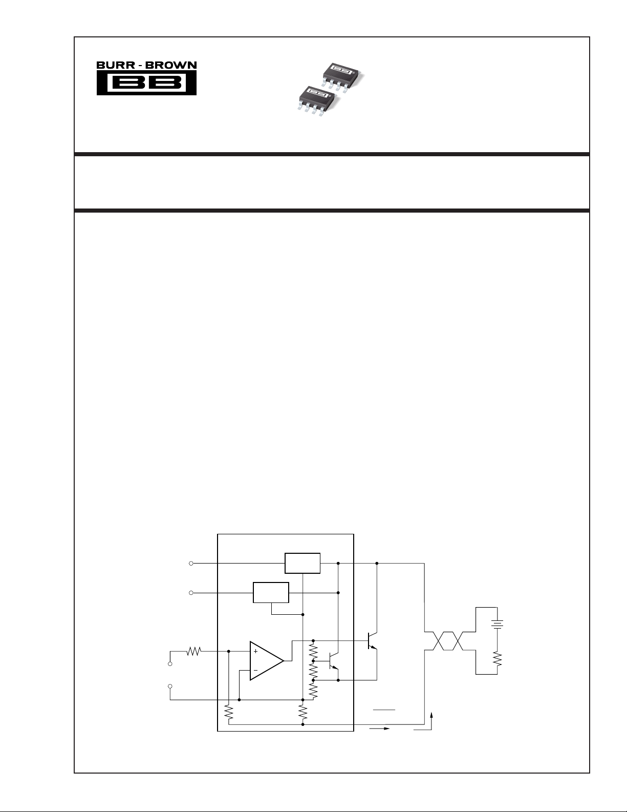
APPLICATIONS INFORMATION
The XTR115 and XTR116 are identical devices except for
the reference voltage output, pin 1. This voltage is available
for external circuitry and is not used internally. Further
discussions that apply to both devices will refer to the
“XTR115/6.”
Figure 1 shows basic circuit connections with representative
simplified input circuitry. The XTR115/6 is a two-wire
current transmitter. Its input signal (pin 2) controls the output
current. A portion of this current flows into the V+ power
supply, pin 7. The remaining current flows in Q1. External
input circuitry connected to the XTR115/6 can be powered
from V
must be returned to I
ground” for input circuitry driving the XTR115/6.
The XTR115/6 is a current-input device with a gain of 100.
A current flowing into pin 2 produces IO = 100 • IIN. The
input voltage at the IIN pin is zero (referred to the I
A voltage input is created with an external input resistor, as
shown. Common full-scale input voltages range from 1V
REG
or V
. Current drawn from these terminals
REF
, pin 3. This I
RET
pin is a “local
RET
RET
pin).
and upward. Full-scale inputs greater than 0.5V are recommend to minimize the effect of offset voltage and drift of A1.
EXTERNAL TRANSISTOR
The external transistor, Q1, conducts the majority of the fullscale output current. Power dissipation in this transistor can
approach 0.8W with high loop voltage (40V) and 20mA
output current. The XTR115/6 is designed to use an external
transistor to avoid on-chip thermal-induced errors. Heat
produced by Q1 will still cause ambient temperature changes
that can affect the XTR115/6. To minimize these effects,
locate Q1 away from sensitive analog circuitry, including
XTR115/6. Mount Q1 so that heat is conducted to the
outside of the transducer housing.
The XTR115/6 is designed to use virtually any NPN transistor with sufficient voltage, current and power rating. Case
style and thermal mounting considerations often influence
the choice for any given application. Several possible choices
are listed in Figure 1. A MOSFET transistor will not improve
the accuracy of the XTR115/6 and is not recommended.
XTR115: 2.5V
XTR116: 4.096V
For IO = 4mA to 20mA
I
IN
With R
V
Input
Circuitry
= 40µA to 200µA
= 20kΩ
IN
= 0.8V to 4V
IN
I
REG
I
REF
R
IN
20kΩ
V
IN
All return current
from I
REG
and I
XTR115
XTR116
V
5V
I
REF
REG
8
V
REF
1
IN
I
IN
2
3
I
RET
R
1
2.475kΩ
Voltage
Reference
A1
+5V
Regulator
R
25Ω
V+
7
B
Q
1
6
E
R
LIM
2
5
I
O
4
I
O
10nF
I = 100 • I
IN
Possible choices for Q1 (see text).
TYPE
2N4922
TIP29C
TIP31B
PACKAGE
TO-225
TO-220
TO-220
V
LOOP
R
L
FIGURE 1. Basic Circuit Connections.
®
5
XTR115, XTR116
Page 6

MINIMUM-SCALE CURRENT
The quiescent current of the XTR115/6 (typically 200µA)
is the lower limit of its output current. Zero input current
(IIN = 0) will produce an IO equal to the quiescent current.
Output current will not begin to increase until IIN > IQ/100.
Current drawn from V
REF
or V
will add to this minimum
REG
output current. This means that more than 3.7mA is available to power external circuitry while still allowing the
output current to go below 4mA.
OFFSETTING THE INPUT
A low scale of 4mA is produced by creating a 40µA input
current. This can be created with the proper value resistor
from V
(Figure 2), or by generating offset in the input
REF
drive circuitry.
XTR115
V
REG
V
40µA
R
62.5kΩ
0 to 160µA
2.5V
0
REF
Voltage
Reference
I
IN
A1
MAXIMUM OUTPUT CURRENT
The XTR115/6 provides accurate, linear output up to 25mA.
Internal circuitry limits the output current to approximately
32mA to protect the transmitter and loop power/measurement circuitry.
It is possible to extend the output current range of the
XTR115/6 by connecting an external resistor from pin 3 to
pin 5, to change the current limit value. Since all output
current must flow through internal resistors, it is possible to
damage with excessive current. Output currents greater than
45mA may cause permanent damage.
XTR115
V
REG
XTR116
V
REF
R
IN
XTR115
V
REG
XTR116
V
REF
I
IN
I
RET
XTR115
V
REG
XTR116
Digital
Control
Optical
Isolation
≈
V
O
D/A
I
O
D/A
5V
I
RET
R
1
2.475kΩ
Digital
Control
Optical
Isolation
≈
µC
PWM
Filter
Out
FIGURE 2. Creating Low-Scale Offset. FIGURE 3. Digital Control Methods.
R
IN
I
RET
®
XTR115, XTR116
6
Page 7

REVERSE-VOLTAGE PROTECTION
The XTR115/6 low compliance voltage rating (7.5V) permits the use of various voltage protection methods without
compromising operating range. Figure 4 shows a diode
bridge circuit which allows normal operation even when the
voltage connection lines are reversed. The bridge causes a
two diode drop (approximately 1.4V) loss in loop supply
voltage. This results in a compliance voltage of approximately 9V—satisfactory for most applications. A diode can
be inserted in series with the loop supply voltage and the V+
pin to protect against reverse output connection lines with
only a 0.7V loss in loop supply voltage.
OVER-VOLTAGE SURGE PROTECTION
Remote connections to current transmitters can sometimes be
subjected to voltage surges. It is prudent to limit the maximum
surge voltage applied to the XTR115/6 to as low as practical.
Various zener diode and surge clamping diodes are specially
designed for this purpose. Select a clamp diode with as low a
voltage rating as possible for best protection. For example, a
36V protection diode will assure proper transmitter operation
at normal loop voltages, yet will provide an appropriate level
of protection against voltage surges. Characterization tests on
several production lots showed no damage with loop supply
voltages up to 65V.
Most surge protection zener diodes have a diode characteristic in the forward direction that will conduct excessive
current, possibly damaging receiving-side circuitry if the
loop connections are reversed. If a surge protection diode is
used, a series diode or diode bridge should be used for
protection against reversed connections.
RADIO FREQUENCY INTERFERENCE
The long wire lengths of current loops invite radio frequency
interference. RF can be rectified by the input circuitry of the
XTR115/6 or preceding circuitry. This generally appears as
an unstable output current that varies with the position of
loop supply or input wiring.
Interference may also enter at the input terminals. For
integrated transmitter assemblies with short connection to
the sensor, the interference more likely comes from the
current loop connections.
8
V
REG
1
V
REF
R
IN
2
V
IN
3
XTR115
I
IN
XTR116
I
RET
V+
7
6
B
E
5
I
O
4
NOTE: (1) Zener Diode 36V: 1N4753A or Motorola
P6KE39A. Use lower voltage zener diodes with loop
power supply voltages less than 30V for increased
protection. See “Over-Voltage Surge Protection.”
0.01µF
Q
1
D
1
FIGURE 4. Reverse Voltage Operation and Over-Voltage Surge Protection.
(1)
1N4148
Diodes
The diode bridge causes
a 1.4V loss in loop supply
voltage.
R
L
must be
PS
V
PS
Maximum V
less than minimum
voltage rating of zener
diode.
®
7
XTR115, XTR116
 Loading...