

Page 1
WM8722
Stereo DAC with Integrated Tone Generator and
Line/Variable Level Outputs
Advanced Informati on, May 2000, Rev 1.5
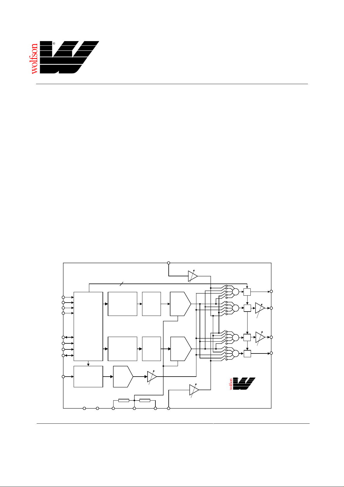
DESCRIPTION
The WM8722 is a high perform ance stereo DAC designed
for audio applications such as digit al TV and set top boxes.
The WM8722 has two stereo analogue outputs, one at line
level and one that includes a digit ally controllable m ute and
attenuator function. An on-board tone generator can be
routed through the line or variable outputs .
WM8722 supports data i nput word lengths from 16-24 bits
and sampling rates up to 96kHz. The WM8722 consists of a
serial interface port, di gi tal interpolation filter, multi-bit s i gma
delta modulator and stereo DAC in a small 20-pin SSOP
package.
The 3 or 2-wire serial MPU compatible control port provides
access to all features including tone generation, on-chip
mute, attenuation and phas e reversal.
The programmable data input port supports glueless
interfaces to popular DSPs, audio decoders and S/PDIF
and AES/EBU receivers.
BLOCK DIAGRAM
FEATURES
• Performance
− 102dB SNR (‘A’ weighted @48kHz)
− THD+N: -90dB @ F.S.
− 5V or 3V supply operation
− Sampling frequency: 8kHz – 96kHz
• 3-wire or 2-wire serial MPU compatible interf ace for
− Input data word; 16/20/24-Bit
− Soft mute
− De-emphasis
− Volume control
• On-board tone generator (1Hz – 32kHz, 0.1 – 25.5s)
• Stereo analogue inputs
• 20-pin SSOP package
APPLICATIONS
• Digital TV
• Digital broadcast receivers
• Set top boxes
MXINL(14)
+12 to -34.5dB, 1.5dB Steps
MONO ATTENUATION CONTROL
4
DIN (17)
BCKIN (19)
LRCIN (18)
SCKI (20)
MD (3)
MC (2)
LATCH (4)
BUSY (5)
TCLK (1)
I2S/SDIF
16,18, 20
OR 24 BITS
SERIAL
INPUT
INTERFACE
TONE
GENERATOR
(6)
(16)
DGND
DVDD
DIGITAL
ATTENUATOR
AND
FILTERS
DIGITAL
ATTENUATOR
AND
FILTERS
TONE
DAC
(10)
AGND
MULTI
BIT
MULTI
BIT
0 TO -46.5dB, 1.5dB
STEPS
(15)
CAP
WOLFSON MICROELECTRONICS LTD
Lutton Court, Bernard Terrace, Edi nburgh, EH8 9NX, UK
Tel: +44 (0) 131 667 9386
Fax: +44 (0) 131 667 5176
Email: [email protected]
http://www.wolfson.co.uk
∑∆
∑∆
(11)
AVDD
(7)
MXINR
MULTI
BIT
SC
DAC
MULTI
BIT
SC
DAC
+12 TO -34.5dB, 1.5dB
STEPS
+
+
L Mix Switches (0-9)
R Mix Switches (0-9)
+
+
0/-6dB
0/-6dB
0/-6dB
0/-6dB
+6 to -73dB,
1dB Steps
(13)LINEOUTL
(12) VAROUTL
(9) VAROUTR
(8) LINEOUTR
WM8722
Advanced Information data sheets contain
preliminary data on new products in t he
preproduction phase of development .
Supplementary data will be published at a
later date.
2000 Wolfson Microelectronics Ltd.
Page 2
WM8722 Advanced Information PIN CONFIGURATION ORDERING INFORMATION
DEVICE TEMP. RANGE PACKAGE
TCLK
MC
MD
LATCH
BUSY
DGND
MXINR
LINEOUTR
VAROUTR
AGND
1
2
3
4
5
6
7
8
9
10
20
19
18
17
16
15
14
13
12
11
SCKI
BCKIN
LRCIN
DIN
DVDD
CAP
MXINL
LINEOUTL
VAROUTL
AVDD
XWM8722EDS -25 to +85oC 20-pin SSOP
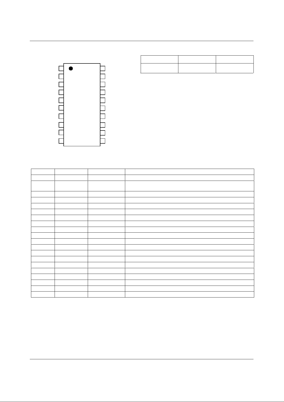
PIN DESCRIPTION
PIN NAME TYPE DESCRIPTION
1 TCLK Digital input
2 MC Digital input
3 MD Digital input
4 LATCH Digital input
5 BUSY Digital I/O
6 DGND Supply
7 MXINR Analogue input
8 VAROUTR Analogue output
9 LINEOUTR Analogue output
10 AGND Supply
11 AVDD Supply
12 LINEOUTL Analogue output
13 VAROUTL Analogue output
14 MXINL A nal ogue i nput
15 CAP Analogue out put
16 DVDD Supply
17 DIN Digital input
18 LRCIN Digital input
19 BCKIN Digital input
20 SCK I Digi tal input
Note: 1. Digital input pins have Schmit t trigger input buffers.
Tone generator master-clock input.
Serial control data cloc k input (SPI mode) or 2-wire cloc k input (2-wire
mode)
Serial control data input (SPI mode) or 2-wire data input (2-wire mode)
Latch enable (SPI mode) or addres s select (2-wire mode).
Interface format i nput pin (0= SPI; 1 = 2-W IRE) or BUSY flag output.
Digital ground supply.
Analogue mixer input (right channel).
Right channel mixer output (variable l evel ).
Right channel mixer output (line level ).
Analogue ground supply.
Analogue positive supply.
Left channel mixer output (line l evel ).
Left channel mixer output (variable l evel ).
Analogue mixer input (left channel).
Analogue internal reference.
Digital positive supply.
Serial audio data input.
Sample rate clock i nput.
Audio data bit clock i nput .
System clock i nput (256 or 384fs).
WOLFSON MICROELECTRONICS LTD AI Rev 1.5 May 2000
2
Page 3
Advanced Information WM8722
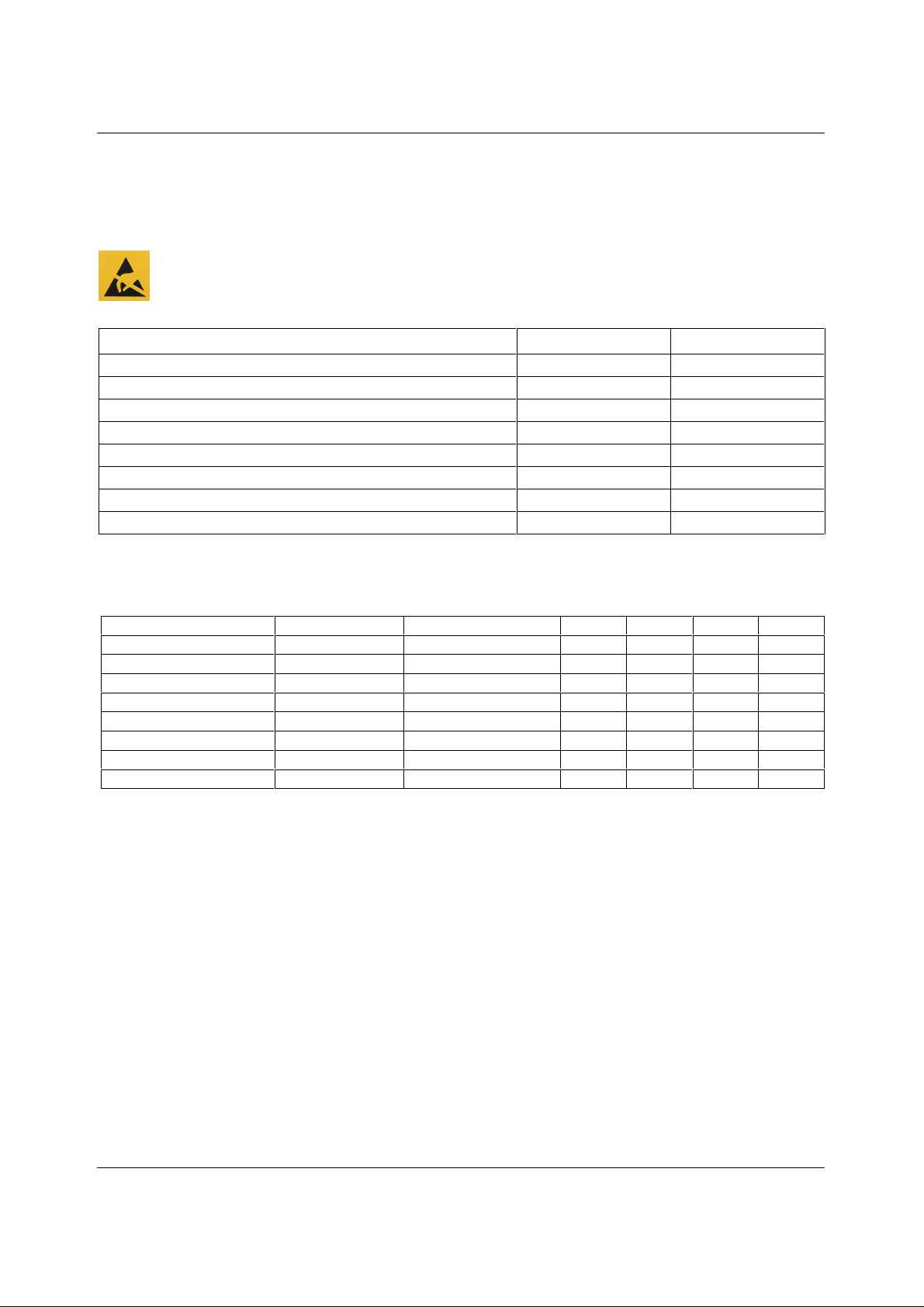
ABSOLUTE MAXIMUM RATINGS
Absolute Maximum Ratings are s tres s rat ings only. P erm anent damage to the device may be c aused by c onti nuously operat ing at
or beyond these limits. Device functional operating lim its and guaranteed performance s pecifications are gi ven under Electrical
Characteristics at the test conditions s pecified
ESD Sensitive Device. Thi s device i s m anufactured on a CMOS process . It i s t herefore generi cally suscept ible
to damage from excessi ve stati c voltages . Proper ES D precautions mus t be tak en during handling and st orage
of this device.
CONDITION MIN MAX
Digital supply voltage
Analogue supply voltage
Voltage range digital inputs
Voltage range analogue inputs
Operating temperature range, T
Storage temperature
Package body temperature (s ol deri ng 10 seconds)
Package body temperature (s ol deri ng 2 seconds)
A
-0.3V +7V
-0.3V +7V
DGND -0.3V DVDD +0.3V
AGND -0.3V AVDD +0. 3V
0°C+70°C
-65°C +150°C
+240°C
+183°C
RECOMMENDED OPERATING CONDITIONS
PARAMETER SYMBOL TEST CONDITIONS MIN TYP MAX UNIT
Digital supply range
Analogue supply range
Ground
Difference DGND to AGND
Analogue supply current
Digital supply current
Analogue supply current
Digital supply current
DVDD -10% 3.3 to 5 +10% V
AVDD -10% 3.3 to 5 +10% V
AGND, DGND 0 V
AVDD = 5V 35 mA
DVDD = 5V 15 mA
AVDD = 3.3V tba mA
DVDD = 3.3V tba mA
-0.3 0 +0.3 V
WOLFSON MICROELECTRONICS LTD AI Rev 1.5 May 2000
3
Page 4
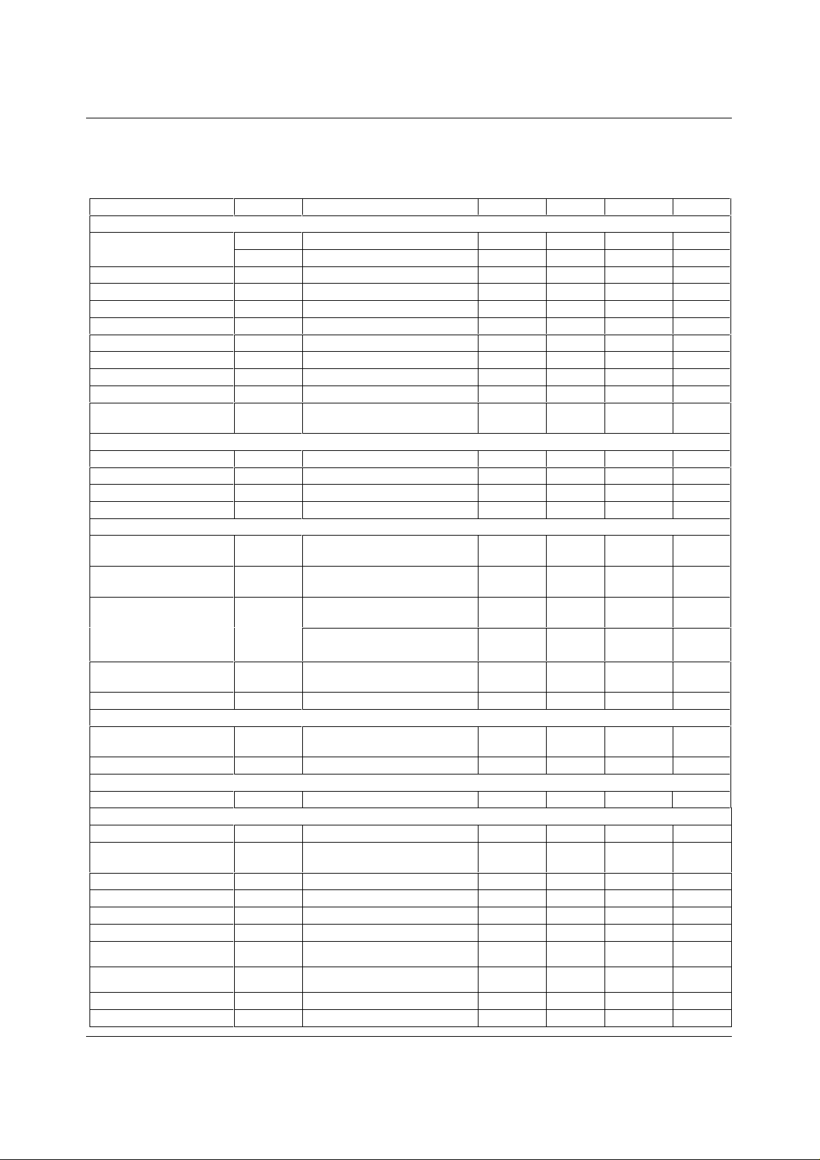
WM8722 Advanced Information ELECTRICAL CHARACTERISTICS
Test Conditions
AVDD, DVDD = 5V, AGND, DGND = 0V , T
PARAMETER SYMBOL TEST CONDITIONS MIN TYP MAX UNIT
DAC Circuit Specifications
SNR (Note 1 and 2)
THD (Note 2)
Dynamic range (Note 2)
Passband
Stopband
Passband ripple
Stopband Attenuation
Channel Separation
Gain mismatch
channel-to-channel
Digital Logic Levels
Input LOW level
Input HIGH level
Output LOW level
Output HIGH level
V
IL
V
IH
V
OL
V
OH
Analogue Output Levels
Output level
Minimum resist ance load
Maximum capacitance
load
Output DC level
Reference Levels
Potential divider
resistance
Voltage at CAP
POR
POR threshold
Analogue Mixer Specifications
SNR
THD
Dynamic Range
Channel Separation
Output voltage
Output current source
Output current sink
= +25oC, fs = 48kHz, SCKI = 256f s unless otherwise stated.
A
AVDD, DVDD = 5V, fs = 48k Hz 92 102 dB
AVDD, DVDD = 3.3V, fs = 48kHz
AVDD, DVDD = 5V, fs = 96k Hz 100 dB
0dB -95 -80
-60dB 102 dB
±0.25dB 0.4535fs dB
-3dB 0.491fs
±0.25 dB
f > 0.55fs - dB
100 dB
±1 ±5 %FSR
0.8 V
2.0 V
IOL = 2mA AVSS + 0.3V
IOH = 2mA AVDD - 0.3V
Into 10kohm, full scale 0dB,
1.1 Vrms
(5V supply)
Into 10kohm, full scale 0dB,
0.66 Vrms
(3.3V supply)
To midrail or AC coupled
1 kohms
(5V supply)
To midrail or AC coupled
600 ohms
(3.3V supply)
5V or 3.3V 100 pF
AVDD/2 V
AVDD to CAP and CAP to AGND
90 kohms
AVDD/2
1.2 1.6 2.0 V
92 100 dB
1V rms output, Into 10kohm, 50pF
-96 -92 dB
load
100 dB
100 dB
Into 10kohm 1.5 Vrms
23 mA
1.5 2 mA
Input voltage, MIXINL/R
MIXINL/R input resistance
MIXINL/R input resistance
AC coupled 2 Vrms
0dB 50 kohm
(at 12dB trim) 20 kohm
WOLFSON MICROELECTRONICS LTD AI Rev 1.5 May 2000
4
Page 5

Advanced Information WM8722
Test Conditions
AVDD, DVDD = 5V, AGND, DGND = 0V , T
= +25oC, fs = 48kHz, SCKI = 256f s unless otherwise stated.
A
PARAMETER SYMBOL TEST CONDITIONS MIN TYP MAX UNIT
Gain mismatch
Frequency Bandwidth
Master volume max gain
Master volume min gain
Master volume step size,
Channel to channel +/-1% +/ -5% % of FSR
0dB gain 100 kHz
567dB
-70 -73 -76 dB
0.7 1 1.3 dB
codes 0 - 47
Master volume step size,
0.5 1 1.5 dB
codes 48 – 79
Master volume gain code
-90 -100 dB
80 – 127 (mute)
Mixer trim max gain
Mixer trim min gain
Mixer trim step size
11 12 13 dB
-32.5 -34.5 -36.5 dB
1.3 1.5 1.7 dB
Tone Generator
SINAD (Note 3)
SINAD
SINAD
SINAD
1Hz to 1kHz tones 65 75 dB
1kHz to 2kHz tones 60 70 dB
2kHz to 4kHz tones 55 65 dB
4kHz to 32kHz tones 50 60 dB
Full scale output voltage;
0dB 2.5 V pk-pk
trims at
Tone Frequency
Tone Duration
Gain adjust range
Gain adjust step size (4
TCLK frequency = 27MHz 1 32767 Hz
TCLK frequency = 27MHz 0.1 25. 5 secs
-46.5 0 dB
1.25 1.5 1.75 dB
bit trim)
Notes: 1. Ratio of output level with 1kHz ful l scale input, to the output l evel with al l zeros into the digital input, measured
‘A’ weighted over a 20Hz to 20kHz bandwidth.
2. All performance measurements done with 20kHz low pass filter. Failure to use such a f ilt er will result in higher
THD+N and lower SNR and Dynamic Range readings than are found in the Electrical Characteri stics. The low
pass filter removes out of band noise; although it is not audible it may affec t dynamic specific ation values.
3. SINAD is ratio of signal to sum of noise, harmonics and spurii, over a bandwidth f rom 1Hz up to either 127x the
tone frequency, or 20kHz, whichever is t he l o wer. (This is to allow for the lower frequency tones havi ng i mages
at 127x and 129x the tone frequency which will fall in the audio band for tones of frequency less than about
20kHz/128).
WOLFSON MICROELECTRONICS LTD AI Rev 1.5 May 2000
5
Page 6
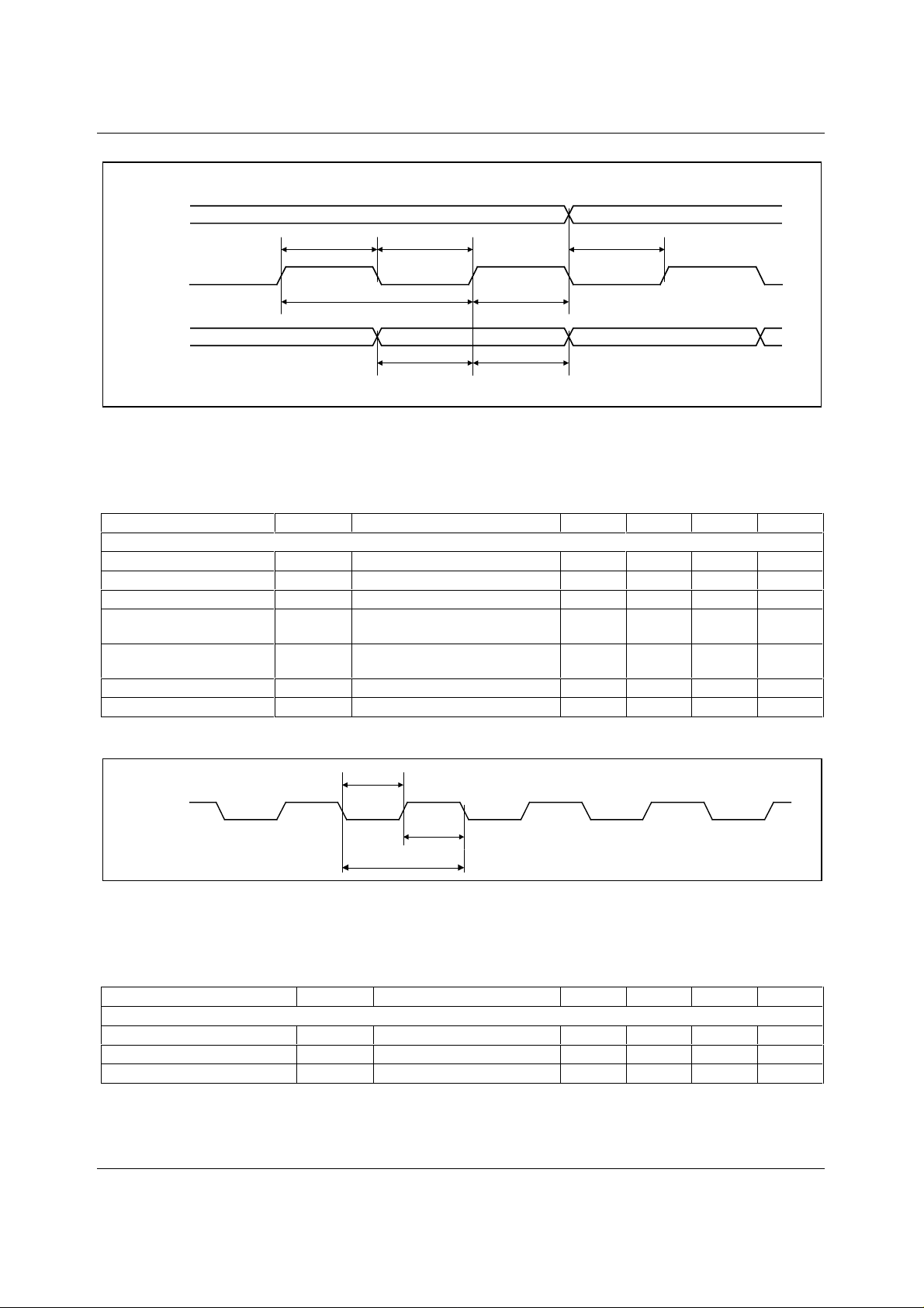
WM8722 Advanced Information
LRCIN
t
BCH
BCKIN
t
DIN
Figure 1. Audio Data Input Timing
Test Conditions
AVDD, DVDD = 5V, AGND, DGND = 0V , T
= +25oC, fs = 48kHz, SCKI = 256f s unless otherwise stated.
A
PARAMETER SYMBOL TEST CONDITIONS MIN TYP MAX UNIT
Audio Data Input Timing Information
BCKIN pulse cycle time
BCKIN pulse width high
BCKIN pulse width low
BCKIN rising edge to
t
t
t
BCY
BCH
BCL
t
BL
LRCIN edge
LRCIN rising edge to
t
LB
BCKIN rising edge
DIN setup time
DIN hold time
t
DS
t
DH
BCY
t
BCL
t
BL
t
DS
t
DH
t
LB
100 ns
40 ns
40 ns
20 ns
20 ns
20 ns
20 ns
t
SCKIL
SCKI
t
SCKIH
t
SCKY
Figure 2. System Clock Timing Requirements
Test Conditions
AVDD, DVDD = 5V, AGND, DGND = 0V , T
= +25oC, fs = 48kHz, SCKI = 256f s unless otherwise stated.
A
PARAMETER SYMBOL TEST CONDITIONS MIN TYP MAX UNIT
System Clock Timing Information
System clock pul se width high
System clock pul se width low
System clock cycle time
t
SCKIH
t
SCKIL
t
SCKY
10 ns
10 ns
27 ns
WOLFSON MICROELECTRONICS LTD AI Rev 1.5 May 2000
6
Page 7
Advanced Information WM8722
t
MLL
t
MHH
LATCH
t
MCY
t
MCHtMCL
t
MLD
t
MLS
MC
t
MDStMDH
MD
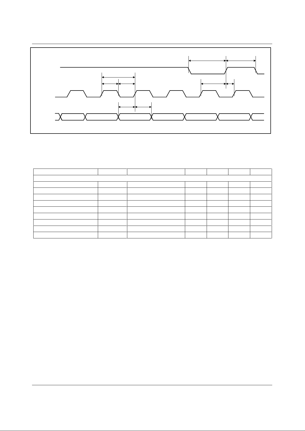
Figure 3. Program Register Input Timing – 3-Wire MPU Serial Control Mode
Test Conditions
AVDD, DVDD = 5V, AGND, DGND = 0V , T
PARAMETER SYMBOL TEST CONDITIONS MIN TYP MAX UNIT
Program Register Input Information
MC pulse cycle time
MC pulse width low
MD pulse width high
MD set-up time
MC hold time
LATCH pulse width low
LATCH pulse width high
LATCH set-up time
LATCH delay from MC
= +25oC, fs = 48kHz, SCKI = 256f s unless otherwise stated.
A
t
MCY
t
MCL
t
MCH
t
MDS
t
MDH
t
MLL
t
MHH
t
MLS
t
MLD
LSB
100 ns
40 ns
40 ns
20 ns
20 ns
20 ns
20 ns
20 ns
20 ns
WOLFSON MICROELECTRONICS LTD AI Rev 1.5 May 2000
7
Page 8
WM8722 Advanced Information
MD
MC
t
3
t
6
t
1
t
t
9
t
5
2
t
7
t
3
t
4
t
8
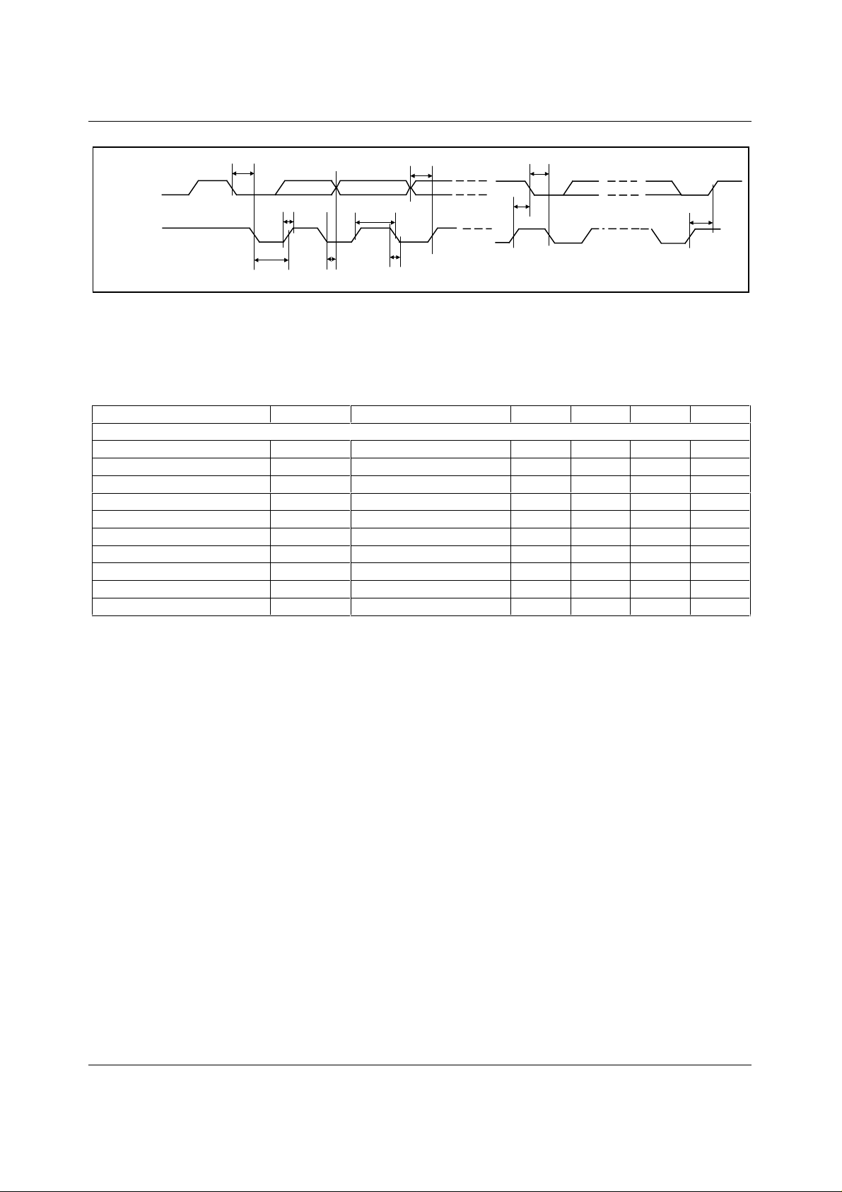
Figure 4. Program Register Input Timing – 2-Wire MPU Serial Control Mode
Test Conditions
AVDD, DVDD = 5V, AGND, DGND = 0V , T
= +25oC, fs = 48kHz, SCKI = 256f s unless otherwise stated.
A
PARAMETER SYMBOL TEST CONDITIONS MIN TYP MAX UNIT
Program Register Input Information
MC Frequency
MC Low Pulsewidth
MC High Pulsewidth
Hold Time (Start Condition)
Setup Time (Start Condit i on)
Data Setup Time
MD, MC Rise Time
MD, MC Fall Time
Setup Time (Stop Condition)
Data Hold Time
t
1
t
2
t
3
t
4
t
5
t
6
t
7
t
8
t
9
0 400 kHz
600 ns
1.3 us
600 ns
600 ns
100 ns
300 ns
300 ns
600 ns
900 ns
WOLFSON MICROELECTRONICS LTD AI Rev 1.5 May 2000
8
Page 9

Advanced Information WM8722
DEVICE DESCRIPTION
WM8722 is a complete low cost s tereo audi o DAC, incl uding digi tal i nterpolat ion f ilt er, m ul ti-bi t s igm a
delta with dither, and switched capac itor multi-bit st ereo DAC and output sm oothing filters. A novel
multi-bit sigma-delta DAC design is used, utilising a 64x oversampling rate, to optimise signal-tonoise performance and increase clock jitter tolerance. The WM8722 also provides an analogue
mixing function, which allows user-s elec table c ontrol over m ixing of an external analogue input s ignal
(line level sources or mi crophone output) with the c onverted output s ignal. The device provides both
line level and variable outputs. The WM8722 contains a high performance sine wave generator
circuit, which can be used t o generate low distortion si nusoidal waveforms of varying frequency and
amplitude. The WM8722 uses a minim um of external component s, with the i nternally generated m idrail references used to provide DC bias of output signals requiring only a si ngle external capaci tor for
decoupling purposes.
The WM8722 is controll ed through a software serial interface. Thi s allows control of variables suc h
as gain levels through each path, t one frequency and duration, and audio data i nterface f ormat. The
software control interface may be operated using either a 3-wire (SPI com patible) or 2-wire MPU
interface. Selection of interface form at is ac hieved by monitori ng the state of BUSY pin at power up.
In 2-wire mode, the ML pin becomes an address selec t, allowing two WM8722 devices to be used on
the same bus.
Operation using system clock of 256fs or 384fs is provided, selection between clock rates being
automatically controlled. Alternatively, the user can select the clock rate through the software
interface. Sample rates (fs) from less than 8ks/s to 96ks/s are allowed, provided the appropriate
system clock is input.
Tolerance of asynchronous word clock jitter is provided, the internal signal proc essing of the device
re-synching to the external LRCIN clock once the phase difference between left-right and system
clocks exceeds half a LRCIN period. During this re-synch period, the overs ampl ing fi lters either mi ss
an audio sample, or repeat the last sample value, so minimising the audibl e ef fects of this operati on.
The interface supports norm al (J apanese ri ght jus ti fied) and I
interface formats, in both packed and unpacked forms. (P acked has exactly the number of serial
clocks corresponding to the number of data bits, per LRCIN period). Additionally the device
automatically detects when it is connected to a 16 bit packed data source (32 serial clocks per
LRCIN) and switches automatically into 16 bit mode. 44.1kHz de-emphasis is supported, with
frequency scaling if other sample rates are used.
2
S (Philips left justified, one bit delayed)
The tone generator circuit uses a high quality sine weighted DAC, and sophist icated noise s haping
techniques to achieve high quality tones with low noise and spurious tone generation. Using the
nominal master tone clock (TCLK) frequency of 27MHz, any frequency from 1Hz to 32kHz m ay be
generated in 1Hz increments. The duration of t he tone burst m ay be program m ed from 0. 1second to
25.5 seconds. The next tone may be pre-programmed during a current tone burst, and is then
loaded, in phase continuous m anner at t he end of t he current tone s o allowing cont inuous generat ion
of varying frequency.
The device is packaged in a small 5.3m m wide 20-pin SSOP package. Single 3V to 5.5V supplies
may be used, the output amplitude scaling with abs olute supply level. Low supply volt age operation
and low current consumption, t he low pin count small package and the analogue mixing features,
make the WM8722 attract ive f or m any cons um er audio appl ic ations , i ncl uding VCD, CD, DV D-Audio,
set-top boxes and digital TV. Separate analogue and digital supply pins are provided, allowing 3V
operation of digital and 5V operation of anal ogue circuits.
ANALOGUE MIXER
The analogue mixer circuits com prise si gnal paths to allow signal switching and gain adjus t for each
of the mixer line-in, DAC output, and tone generator signals. Additionally, mono signals can be
created using the completely flexible switching arrangement s, and 6dB attenuati on switching c ircuit s.
Individual control bits are provided for each of the 5 switch inputs to each summ ing stage in the
mixer, each signal path theref ore being individuall y controllabl e. Any com binati on of out put s ignals is
therefore permissible. Fixed output level line outputs and volume adjusted variable output level
outputs are provided.
WOLFSON MICROELECTRONICS LTD AI Rev 1.5 May 2000
9
Page 10

WM8722 Advanced Information
TONE GENERATOR DAC
The tone generator comprises a di gi tal frequency synthesiser, which is used to create a clock at 128x
the required tone frequency, and a 128 step per cycle, s ine weighted DAC, which convert s the cloc k
into one of three tone types. An anal ogue programmable gain st age follows the DAC, allowing gain
adjustment of the tone amplitude. Noise shaping techniques are used to c reate minimal spurious
components in the frequency synthesiser.
The WM8722 can generate three different tone types. The default setting is a sinusoidal tone.
Square waves are generated by setting the SQR bit . Alternatively, a two-tone output that generates
one cycle at the chosen frequenc y, f ollowed by two cycles at twice t hat frequenc y c an be s elec ted by
setting the F2F bit. This facilit y may be used in sine or square wave modes.
The frequency of the resulting tone is controllable with 1Hz resolution, over a range of 1Hz to
32.767kHz, based on a TCLK frequency of 27MHz. Alternative tone c lock frequenc ies m ay be us ed if
required. For example the DAC SCLK frequency m ay be used, but in these cases the frequency
range and resolution will change by the ratio of the clock used, to the nominal 27MHz clock specified.
The duration of the selected tone is programmed via the serial int erface. Once both the frequency
and the duration have been set to non-zero values, the tone generation com mences. Onc e the tone
generator has started running, the next tone f requency and duration may be programm ed ready to
start as soon as the c urrent tone finishes. Under this condition the tones are phase continuous, and a
BUSY flag is set on the BUSY pin, which now becomes a CMOS output, overdriving any pull -up or
down resistor placed on the pin to select t he interface form at at power-up. After a tone frequenc y of
duration has been written, it m ay be over writt en with a new value if desired.
At the conclusion of a t one burst, the circui t ensures that at the end of the duration t ime of the last
tone, the tone continues to the next zero crossing point to ensure DC offsets are not created. A
control bit (TFIN) is provided which allows select ion of t he m ethod of com pl etion of the burs t: If set to
1, the burst complet es at the next zero crossi ng. If left at 0, the burst completes a whole number of
sinusoids, avoiding potent i a l probl ems with DC levels changing acros s AC coupling capacitors.
SYSTEM CLOCK
Whilst tones are being generated, writing either new frequency or new duration, will cause the
subsequent burst to be generated phas e continuously with the current burst. If a durati on value of 0
is written during a burst, the current burst will stop immediately (at the next zero cross or full cycle
complete point as sel ected by TFIN).
If the current burst com pletes, and no new duration of frequency have been set, the tones stop and
the duration value is reset to zero. The frequency s etting is mai ntained in volatile mem ory. If a new
duration is programmed, then the tone generator will re-start with the previously programmed
frequency. If a new frequency is des ired, the frequency is simpl y programmed before the duration,
the tone commenc i ng when the durati on i s written.
The system clock for the WM8722 must be either 256fs or 384fs where fs is the audio sampling
frequency (LRCIN), typically 32kHz, 44.1kHz, 48kHz or 96kHz. The system c lock is used t o operate
the digital filters and t he noi se shaping circuits.
WM8722 has system cloc k detec tion ci rcuitry t hat autom atic ally determ ines the rel ationshi p between
the system clock frequency and the sampli ng rate (to within 8 system cl ocks). If greater than 8 clocks
error, then the interface shuts down the DA C and mutes the output. The system cloc k should be
synchronised with LRCIN, but W M8722 is tolerant of phase di fferences or jitter on t his clock . S evere
distortion in the phase difference between LRCIN and the system clock (for example c aused by too
many or too few system clocks received per LRCIN period) will be detected, and cause the device to
automatically re-synchroni se. If the externally applied LRCIN slips in phase by m ore than half the
internal LRCIN period, which is derived from the master clock, then the int erface resynchronises.
During re-synchronisation, the WM8722 will either repeat the previous sample or drop the next
sample depending on the nature of the phase slip. This will ens ure t here is no dis cernible clic k at t he
analogue outputs during re-synchronis at i on.
WOLFSON MICROELECTRONICS LTD AI Rev 1.5 May 2000
10
Page 11
Advanced Information WM8722
11.2896
SAMPLING RATE
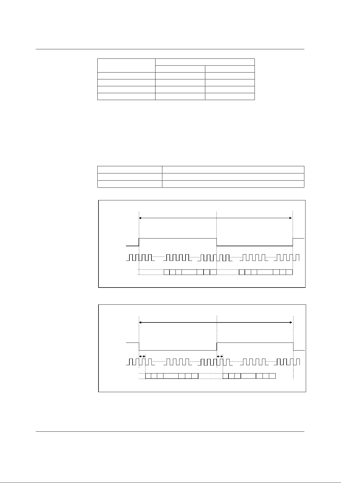
Table 1 System Clock Frequencies versus Sampling Rate
AUDIO DATA INTERFACE
The serial data interface to W M8722 is full y compat ible with both norm al (MSB f irst, right-jus tified) or
2
S interfaces. Data may be packed (number of seri al BLCKS per LRCIN period i s exactly 2 times the
I
number of data bits, i.e. normally 32 in 16 bi t mode) or unpacked (more t han 32 BCLKs per LRCIN
period.
The WM8722 will automatically detect 16-bit packed data being sent to the device in normal mode,
and accept the data in this i nput format accordingly.
Table 2. Serial Interface Formats
SYSTEM CLOCK FREQUENCY (MHZ)
(LRCIN)
256fs 384fs
32kHz 8.192 12.288
44.1kHz
16.9340
48kHz 12.288 18.432
96kHz 24.576 36.864
2
I
S MODE DESCRIPTION
0 Normal format (MSB-f i rst, right justif i ed)
1I
2
S format (Philips serial data protocol )
1/fs
LEFT CHANNEL RIGHT CHANNEL
LRCIN
BCKIN
DIN
123
MSB MSB LSB
Figure 5. Normal Data Input Timing
LEFT CHANNEL RIGHT CHANNEL
LRCIN
BCKIN
DIN
123
MSB
Figure 6. I2S Data Input Timing
123
MSB LSBLSB
123
nn-1n-2
nn-1n-2
nn-1n-2
LSB
1/fs
nn-1n-2
WOLFSON MICROELECTRONICS LTD AI Rev 1.5 May 2000
11
Page 12
WM8722 Advanced Information
MODES OF OPERATION
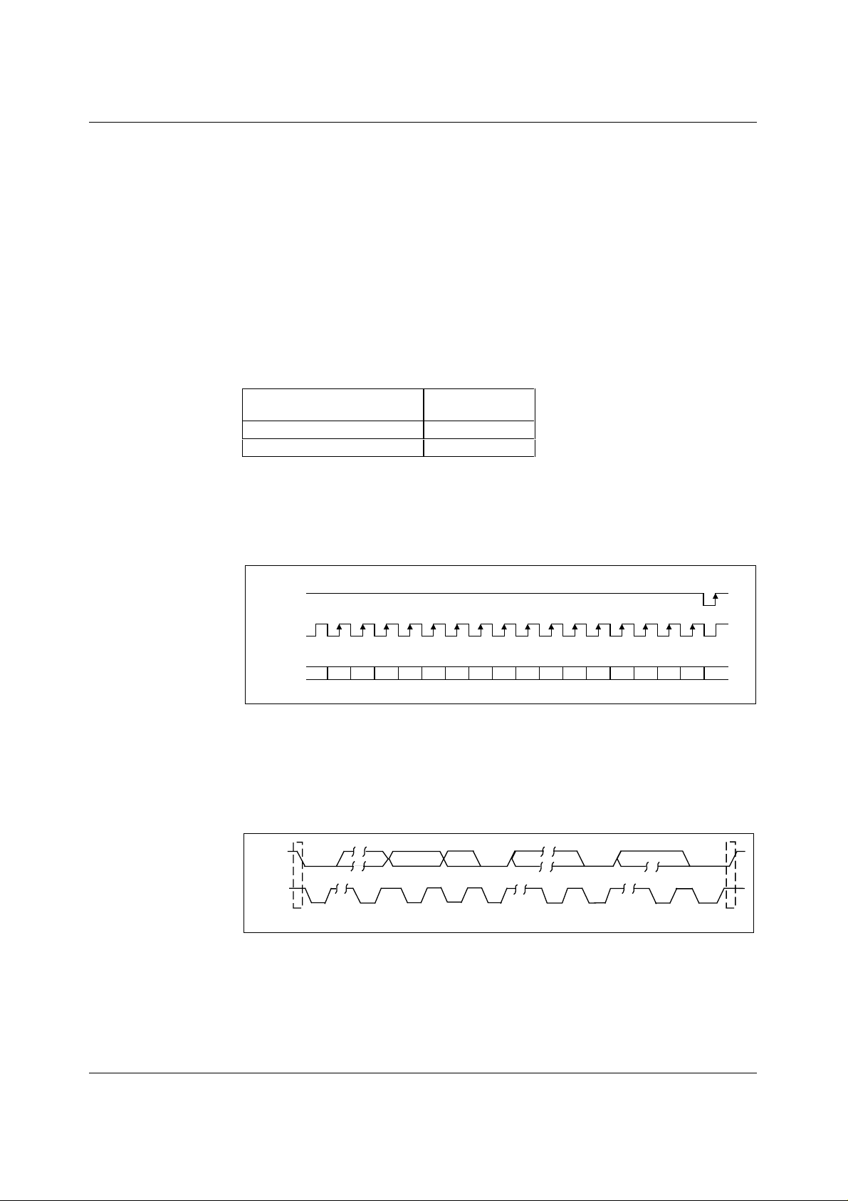
The software control interface m ay be operat ed usi ng either a 3-wire (SP I-c om pati ble) or 2-wire MPU
interface. Selecti on of interface format i s achieved by monitoring the s t ate of BUSY pin at power up.
In 3-wire mode, MD is used for the program data, MC is used to clock in the program data and
LATCH is used to latch in the program data. In 2-wire mode, MD is used for serial data and MC is
used for serial clock . In 2-wire mode, the LATCH pin allows the user to select one of two addresses.
SELECTION OF SERIAL CONTROL MODE
The serial control interfac e may be selec ted to operate in eit her 2 or 3-wire modes. This is achieved
by setting the state of the BUSY pin at power-up with a weak, external pul l-up or pull-down resist or
(typically 10k). This pin i s an input at power up, and its state selec ts the type of i nput format. The
value input at power-up is sampled and st ored internally. This allows t he BUSY pin to be used as an
output when tone generation has been enabled. This s tored value is only reset when the device is
powered off.
BUSY PIN (TONE
GENERATION NOT ENABLED)
INTERFACE
FORMAT
03 wire
12 wire
Table 3. Control Interface Mode Selection
3-WIRE (SPI COMPATIBLE) SERIAL CONTROL MODE
The WM8722 can be controlled us ing a 3-wire serial int erface. MD is used f or the program data, MC
is used to clock i n the program data and LATCH is use to latch in the program dat a. The 3-wire
interface protocol is s hown in Figure 7.
LATCH
MC
MD
B15 B6B7B8B9B10B11B12B13B14 B1B2B3B4B5 B0
Figure 7. 3-Wire Serial I nterface
2-WIRE SERIAL CONTROL MODE
The WM8722 supports a 2-wire MPU serial interface. The device operates as a slave device only.
The WM8722 has one of two slave addresses that are selected by setting the state of pin 5,
(LATCH).
MD
MC
START
ADDR
R ADDR R/W ACK ACK
ACK
DATA B7-0DATA B15-8
STOP
Figure 8. 2-Wire Serial I nterface
WOLFSON MICROELECTRONICS LTD AI Rev 1.5 May 2000
12
Page 13

Advanced Information WM8722
LATCH STATE Address
1 1000001
0 1000000
To control the WM8722 on the bus, the master must ini tiate a data transfer by establishi ng a start
condition, defined by a high-to-low transition on MD whilst MC remains high. This indic ates that an
address and data transfer will follow. All peripherals respond to the s tart condition and shift the next
eight bits (7-bit address + R/W bit). The trans fer is MSB first. The peripheral that recognises the
transmitted address responds by pulling the data line low during the ninth cl ock pulse (acknowledge
bit). All other devices withdraw from the bus and maintain an idle condition once the appropriate
peripheral has been recognised. The idle c ondition is where the device monitors the MD and MC
lines waiting for a start condition and the correct trans mitted address. The R/W bit determines the
direction of data transfer. The WM8722 is a write only device and only responds to the R/W bit
indicating a write.
The WM8722 acts as a s tandard slave devic e on the bus. The data on the MD is clock ed in by MC.
The first 6 bits (which must be 100000) are clocked into the W M8722 followed by a programm able
address bit to select one of the t wo available addresses. The eighth bit of the address byt e is the
R/W bit. The W M8722 checks this bit and responds if it is a write. If the c orrect address is sent by
the master, the WM8722 acknowledges the bus m aster (ACK) and pulls the bus low. The next byte is
the register address. Each subsequent byte of data is separated by an acknowledge bit.
A stop condition is def i ned when there is a low-to-high transition on MD when MC is high.
If a stop or start condi tion is detected out of s equence at any point in t he data transfer, the device
jumps to the idle condi tion.
SERIAL CONTROL OPERATION
Control of the various modes of operation is sof tware cont rol over the 2 or 3-wire seri al int erfac e. The
following functions m ay be controlled via the serial cont rol i nterface:
FUNCTION OPTIONS SOFTWARE CONTROL
Input audio data format Normal format
Input Word Length 16
De-emphasis selection On
Operation enable (OPE)
(power down)
Analogue output mode L, R, mono, Mute Stereo (1001)
Mute On (Muted)
Input LRCIN polarity Lch/Rch = Hi/Lo
Master Volume Control Lch, Rc h i ndi vidually
2
I
S format
20
24
Off
Enable
disable
Off (Un-muted)
Lch/Rch = Lo/Hi
Lch, Rch both
DEFAULT VALUE
Normal format (0)
16 bit (0)
Off (0)
Enabled (0)
Off (0)
Lch/Rch = Hi/Lo (0)
0dB (1111001)
Lch, Rch individually (0)
WOLFSON MICROELECTRONICS LTD AI Rev 1.5 May 2000
13
Page 14

WM8722 Advanced Information
FUNCTION OPTIONS SOFTWARE CONTROL
DEFAULT VALUE
DAC digital volume Lch, Rch individually
Lch, Rch common
Mixer Volume Control Lch, Rch indivi dual l y
Lch, Rch both
Mixer Output Selection 5 switches for each of left and
right, mix and volume paths,
individually controlled, or both
together, and with –6dB gain
option for mono modes
Tone amplitude 0 to –46.5dB in 1.5dB steps
plus mute
Tone frequency 1 to 32767Hz in 1Hz steps
(based on 27MHz TCLK)
Tone duration 0.1 to 25.5secs in 0.1sec
steps
Tone Finish Behaviour
(TFIN)
Tone Waveform Sine or square wave 0 = sine
0dB (111111)
Lch, Rch individually (0)
0dB (10111)
Lch, Rch individually (0)
Normal stereo
(11100) MLMX left mux
(11100) MLVMX left mux
(11100) MRMX right mux
(11100) MRVMX right mux
M6DB bits all 0 (gain 0dB)
0dB (11111)
0 = disabled
0 = disabled
1 = Full cycle sine wave
0 = next zero cross
1 = square wave
Tone Burst f or 2f 0 = f
Table 4. Control Functions
1 = 2f
WOLFSON MICROELECTRONICS LTD AI Rev 1.5 May 2000
14
Page 15
Advanced Information WM8722
REGISTER MAP
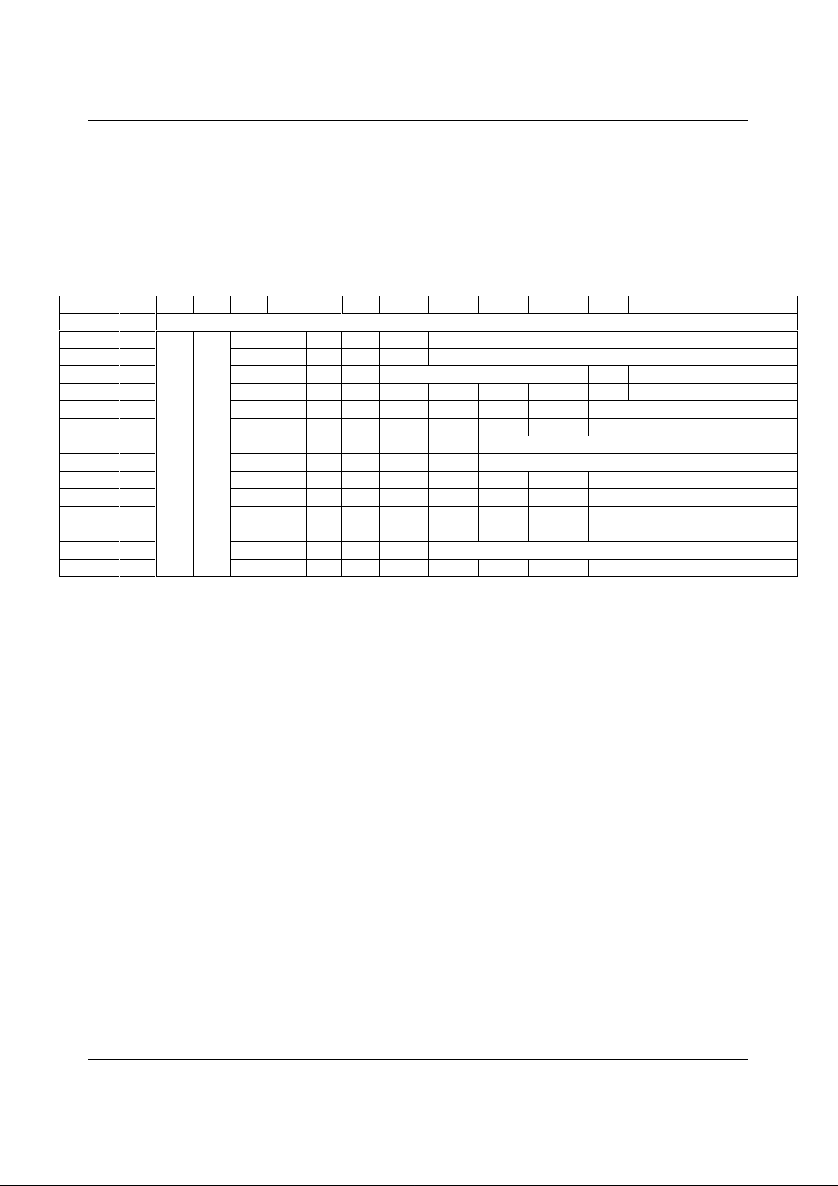
The WM8722 controls t he device f unct ions usi ng 15 program regist ers, eac h of which is 16-bi ts l ong.
These registers are all loaded via t he serial control interface in ei ther 2 or 3-wire mode.
There are two type of control word; either TFRQ, the tone frequency word, which is a single address
bit followed by 15 data bits, or other types, which have 6 address bits, and 10 bits of dat a. Other
types have the lead address bit invert ed com pared t o TFREQ words, al lowing use of a s ingle write t o
load the required frequency.
REG B15 B14 B13 B12 B11 B10 B9 B8 B7 B6 B5 B4 B3 B2 B1 B0
TFREQ
R0 0 0 0 0 0 LDL
R1 0 0 0 0 1 LDR
R2 0 0 0 1 0
R3 0 0 0 1 1
R4 0 0 1 0 0 BOTH res res MUTE
R5 0 0 1 0 1 BOTH res res MUTE
R6 0 0 1 1 0 BOTH ZCEN
R7 0 0 1 1 1 BOTH ZCEN
R8 0 1 0 0 0 BOTH res res M6DB0
R9 0 1 0 0 1 BOTH res res M6DB1
R10 0 1 0 1 0 BOTH res res M6DB2
R11 0 1 0 1 1 BOTH res res M6DB3
R12 0 1 1 0 0 res
R13 0
1
RESERVED
RESERVED
1 1 0 1 F2F SQR TFIN MUTE
Table 5. Mapping of Program Registers
res
F[14:0]
DAL [7:0]
DAR[7:0]
PL[3:0]
res res res res res ATC LRP I2S
IW1 IW0 PWD DE MU
MTRIML[4:0]
MTRIMR[4:0]
LVOL[6:0]
RVOL[6:0]
LMXSEL(4-0)
RMXSEL(4-0)
LVMXSEL(4-0)
RVMXSEL(4-0)
TTIM[7:0]
TVOL[4:0]
WOLFSON MICROELECTRONICS LTD AI Rev 1.5 May 2000
15
Page 16

WM8722 Advanced Information
REGISTER
NAME
REG
ADDRESS
BIT NAME DESCRIPTION DEFAULT VALUE
TFREQ 1 F[14:0] Tone f requenc y val ue
Register 0 000 0000 DAL[7:0]
LDL
Register 1 000 0001 DAR[7:0]
LDR
DAC attenuation data for left channel
Attenuation data load control for left channel
DAC attenuation data for right channel
Attenuation data load control for right
channel
Register 2 000 0010 MU
DE
PWD
IW[1:0]
PL[3:0]
Register 3 000 0011 I2S
LRP
ATC
Register 4 000 0100 MTRIML[4:0]
MUTE
Register 5 000 0101 MTRIMR[4:0]
MUTE
Register 6 000 0110 LVOL[6:0]
Left and right DACs soft mute control
De-emphasis control
Power off control
Input audio data bit length select
Output mode select
Audio data format select
Polarity of LRCIN (pin 7) select
Attenuator control
Left mixer 1 attenuation data
Left mixer mute
Right mixer 1 attenuation data
Right mixer mute
Left volume 2 attenuation data
ZCEN
BOTH
Register 7 000 0111 RVOL[6:0]
Right volume 2 attenuation data
ZCEN
BOTH
Register 8 000 1000 LMXSEL
M6DB0
Left mixer output mux control
M6DB for left mix output
BOTH
Register 9 000 1001 RMXSEL
M6DB1
Right mixer output mux control
M6DB for right mix output
BOTH
Register 10 000 1010 LVMXSEL
M6DB2
Left variable output mux control
M6DB for left variable output
BOTH
Register 11 000 1011 RVMXSEL
M6DB3
Right variable output mux control
M6DB for right variable output
BOTH
Register 12 000 1100 TTIM[7:0] Tone duration
Register 13 000 1101 TVOL[4:0]
MUTE
TFIN
SQR
F2F
Tone amplitude
Tone mute
Tone burst finish on zero cross
Tone sine or square wave
Tone one cycle at F, two cycle at 2xF
Table 6. Internal Register Mapping
000 0000 0000 0000
111 1111 (0dB)
0
111 1111 (0dB)
0
0 (not muted)
0 (de-emph off)
0 (power on)
00 (16 bit)
1001 (normal stereo)
0 ( NORMAL format)
0
0
10111 (0dB)
0 (not mute)
10111 (0dB)
0 (not mute)
1111 001 (0dB)
1111 001 (0dB)
11100 (normal stereo)
0 (0dB)
11100 (normal stereo)
0 (0dB)
11100 (normal stereo)
0 (0dB)
11100 (normal stereo)
0 (0dB)
000 0000 (no tone)
11111 (max output)
0 (not muted)
0 (finish on full cycle)
0 (sine wave)
0 (normal F)
REGISTER TFREQ
TONE FREQUENCY
This is the special regi ster of 15 bit length with a s ingle bit address, to allow values for the selected
tone frequency from 1Hz to 32767Hz t o be writt en i n one word. Writing 0 turns off the tone.
F
TONE
= (F
TCLK
x T
FREQ [15:0]
WOLFSON MICROELECTRONICS LTD AI Rev 1.5 May 2000
)/27x10
6
16
Page 17
Advanced Information WM8722
REGISTER 0/1
DAC OUTPUT ATTENUATION
A digital attenuator is provided to allow the levels of DAC signals to be attenuated in the digital
domain.
Register 0 (A[1:0] = 00) is us ed to control left channel attenuation. Bit s 0-7 (AL[7:0]) are used to
determine the attenuation l evel . The level of attenuation is given by:
Attenuation = [20.log10 (At t enuation_Data/255)] dB
Bit 8 in register 0 (LDL) is us ed to control the loading of at tenuation dat a in B [7:0]. When LDL is set
to 0, attenuation data will be loaded into AL[7:0], but it will not affect t he attenuation level until LDL is
set to 1. LDR in register 1 has the same function for ri ght channel attenuation.
Attenuation levels are controlled by setting t he register set AL[7:0] (left channel) or AR[7:0] (right
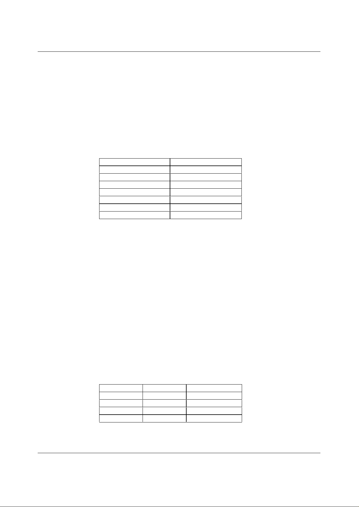
channel). Attenuation levels are given in Table 7.
AX[7:0] ATTENUATION LEVEL
00h - ∞ dB (Mute)
01h -48.16 dB
::
::
::
FEh -0.034 dB
FFh 0dB
Table 7. Attenuation Control Levels
REGISTER 2
Register 1 (A[1:0] = 01)is used to control right channel attenuation in a similar manner.
SOFT MUTE
Soft mute is controlled by setting bit 0 in register 2 (A[1:0]=10). A high level on bit 0 will cause the
DAC outputs to be muted, the effect of which is t o ramp the s ignal down in the digit al domai n so that
there is no discernible cl i ck.
DIGITAL DE-EMPHASIS
Bit 1 (DE) in register 2 (A[1:0]=10) is used to control digital de-emphasis. A low level on bit 1
disables de-emphasis whils t a high level enables de-emphasis .
POWER OFF CONTROL
Bit 2 (PWD) in regi ster 2 is used for operation control. With P WD = low (default) the device functions
normally. With PWD = high the device is disabled and the outputs are held at midrail. Current
consumption of the di gital sect ion is mi nimised, but analogue bias s ections rem ain active in order to
preserve DC levels.
INPUT WORD RESOLUTION
Bits 3 and 4 of register 2 (IW [1:0]) are used to determi ne the input word resolution. The WM8722
supports 16-bit, 18-bit, 20-bit and 24-bit word formats.
BIT 4 (IW1) BIT 3 (IW0) INPUT RESOLUTION
00
01
10
11
Table 8. Input Data Resolution
16-bit Data Word
20-bit Data Word
24-bit Data Word
18-bit Data Word
WOLFSON MICROELECTRONICS LTD AI Rev 1.5 May 2000
17
Page 18

WM8722 Advanced Information
DAC OUTPUT CONTROL
Bits 5, 6, 7 and 8 (PL[3:0]) of register 2 are used to control the output format.
PL0 PL1 PL2 PL3 LEFT OUTPUT RIGHT OUTPUT NOTE
0000
0001
0010
0011
0100
0101
0110
0111
1000
1001
1010
1011
1100
1101
1110
1111
Table 9. Programmable Output Format
MUTE MUTE Mute Both Channels
MUTE R
MUTE L
MUTE (L + R)/2
RMUTE
RR
R L Reverse Channels
R(L + R)/2
LMUTE
L R Stereo Mode
LL
L(L + R)/2
(L + R)/2 MUTE
(L + R)/2 R
(L + R)/2 L
(L + R)/2 (L + R)/2 Mono Mode
REGISTER 3
REGISTER 4/5
AUDIO DATA INPUT FORMAT
WM8722 allows maximum flexibility over the control of the audio data interface, allowing selection of
format type, word length, and sample rates.
DIGITAL AUDIO SERIAL PROTOCOL
A low on bit 0 sets the form at to Normal (MSB-first , ri ght justified Japanese f ormat), whilst a high sets
the format to I
2
S (Philips serial data protocol).
AUDIO INTERFACE CLOCKS
Bit 1 (LRP) of register 3 is used to control the polarity of LRCIN (sample rate cl ock). W hen bit 1 is
low, left channel data is assum ed when LRCIN is in a hi gh phase and right c hannel data is assum ed
when LRCIN is in a low phase. When bit 1 is high, the polarity assumption is reversed.
ATTENUATOR CONTROL
Bit 2 in register 3 (A1[1: 0] = 11) is used to control the attenuator (ATC). W hen ATC is high, the
attenuation data loaded in program regis ter 0 is used f or both the left and the right channels . W hen
ATC is low, the attenuation dat a for each register is applied separately to left and right channels .
ANALOGUE MIXER TRIM
Bits 0-4 of register 4, MTRI ML[0:4], set the gai n level of the f irst s tage of analogue mi xing on the left
channel. The 5-bit register sel ect s 1. 5 dB inc rem ents of t he MIXINL signal, over a range of +12dB to
–34.5dB. A 6
Similarly, bits 0-4 of register 5, MTRIMR[0: 4], set the at tenuation level of the firs t stage of analogue
mixing on the right channel. The 5-bit regi st er allows 1. 5 dB inc rem ents of t he MIXINR signal, over a
range of +12dB to –34.5dB. A 6
th
bit, MUTE, controls m uting of the signal when set high.
th
bit, MUTE, controls m uting of the signal when set high.
WOLFSON MICROELECTRONICS LTD AI Rev 1.5 May 2000
18
Page 19

Advanced Information WM8722
BOTH
In register 4 and 5, a further bit B OTH is availabl e: When a write is made to eit her regis ter 4 or 5 and
BOTH is set high, then the same value written to the register will also be written into the other
register. This allows both Left and Right channel gains to be updated simultaneously, hal ving the
number of serial writes required, (s im plifying gai n ramping, for example) provided t hat the sam e gain
is needed for both channels.
REGISTER 6/7
VOLUME CONTROL
Bits 0-6 of register 6, LV OL[6:0], control gain applied to the variable level out put VAROUTL. This 6bit register controls 1.0 dB increments of t he vol ume, over a range of +6 dB to –73 dB.
Similarly bits 0-6 of register 7, RVOL[6:0], control the gain applied to the variable level output
VAROUTR. Value 1111111 sets maxim um, i.e. 6dB gain. Code 48 sets minim um gain. Values les s
than code 48 apply mute to the gai n stage. (i.e. set volume to 000 0000 to achieve mute)
ZCEN
A zero cross detect circuit is provided, so t hat vol um e cont rol values are only updat ed when the input
signal to the gain stage is close to t he analogue ground level, mini mising cli cks and zi pper noise as
the gain values are changed. This circuit has no time out so if DC l evels are being applied t o the gai n
stage input, then the gain will not be updated. This zero cros s func ti on is enabled when the ZCEN bit
is set high during a volume regi ster write. If there is concern that a DC level may have bloc ked a
volume change (one made with ZCEN set high), then a subsequent volume write of the s ame value,
but with the ZCEN bit set low will force a volume update regardless of the DC level.
BOTH
In register 6 and 7, a further bit BOTH is available. When a write is made to either regist er 6 or 7 and
BOTH is set high, then the same value written to the register will also be written into the other
register. This allows both Left and Right channel gains to be updated simultaneously, hal ving the
number of serial writes required, provi ded that the same gain is needed f or both channels.
REGISTER 8, 9, 10, 11
ANALOGUE MIXER OUTPUT SELECTION
The WM8722 allows software controllable selec ti on of s ignal out puts . The WM8722 allows 2 outputs
per channel, with one output at line level, and another output at variable level, according to the
LVOL[6:0] and RVOL[6:0] attenuat ion register s ettings. I n addition, the us er may selec t whether the
left or the right signal, converted in the DAC, is m i xed with the corresponding mixer input or not.
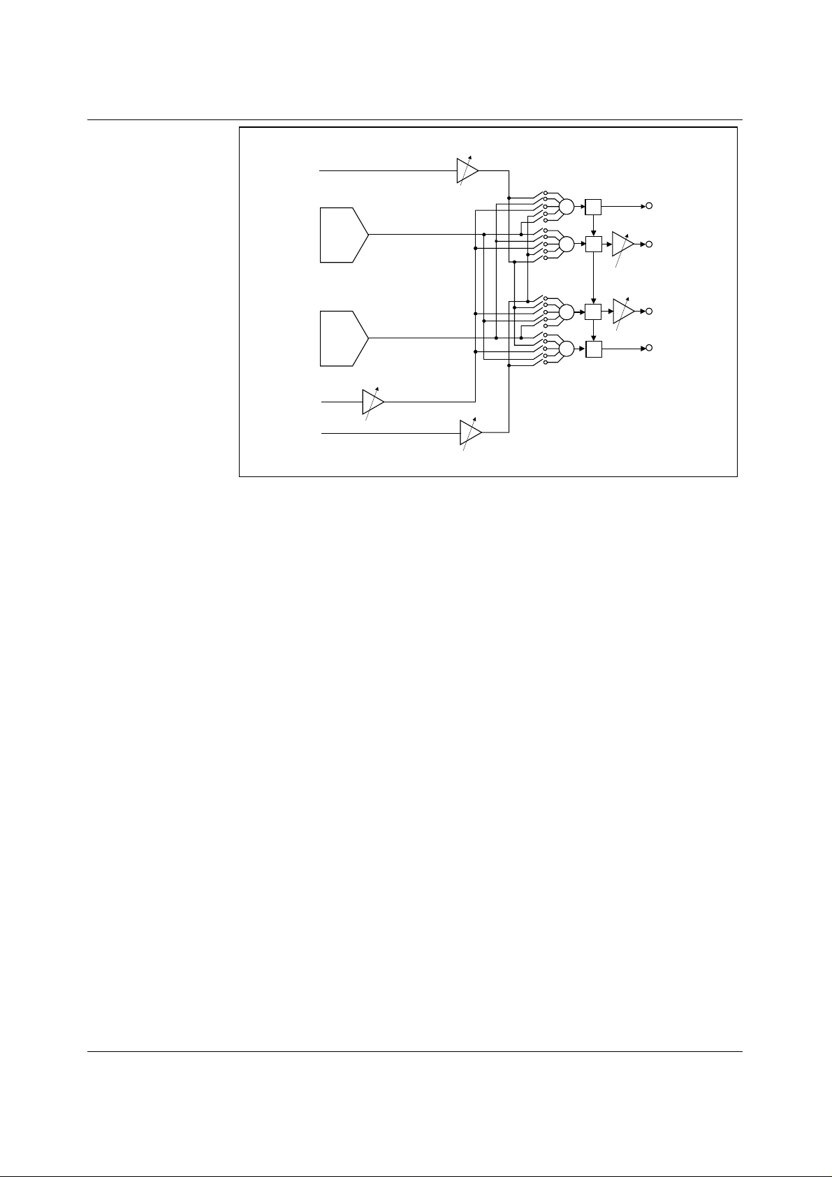
This switching scheme is detailed in Figure 9, with 10 different select signals per channel, 5 eac h for
each Mux: Each Mux therefore has 5 input signals; DACL, DACR, MIXL, MIXR and TONE. This
allows completely flexible sel ection of signal paths, bot h mono and stereo outputs, on any output.
Table 10. MUX(4:0) mux control swi tches
If mono outputs are selected, the gain through the summer amplifiers may be reduced by 6dB if
required by setting the appropriate M6DB bits. S imilarly left and right channels may be completely
swapped.
MUX CONTROL BITS MXSEL(4:0) SIGNAL SELECTED WHEN HIGH IS SET
0
1
2
3
4
DAC sum enable
MIXIN sum enable
TONE in sum enable
Opposite channel DAC sum enabl e
Opposite channel MIXIN sum enable
WOLFSON MICROELECTRONICS LTD AI Rev 1.5 May 2000
19
Page 20
WM8722 Advanced Information
MXINL
LINEOUTL
VAROUTL
VAROUTR
LINEOUTR
TONE
DAC
MXINR
LEFT
DAC
RIGHT
DAC
+
+
L Mix Switches (0-9)
R Mix Switches (0-9)
+
+
0/-6dB
0/-6dB
0/-6dB
0/-6dB
Figure 9. Output Mixer Configuration
M6DB
In each of the 4 MUX control registers there is an M6DB bit relevant t o that channel. Setti ng M6DB
high reduces the relevant output s i gnal by 6dB.
BOTH
When a write to any MXSEL register is made with the BOTH bit set hi gh, then the c omplementary
channel MXSEL register for the other channel is updated with the same value. For example, if
RVMXSEL is updated and BOTH is set, t hen LVMXSEL is updat ed with the same value, but the
RMXSEL and LMXSEL registers (the non variable output path m uxes) are NOT updated.
REGISTER 12
TONE DURATION
Bits 0-7 of register 12 sets the duration of t he tone burs t. Writing to the regist er with a non-zero value
starts the tone burst. Wring zero to this register stops the tone.
T = (2.7x10
6
x TTIM[7:0])/ F
TCLK
REGISTER 13
TONE GENERATOR GAIN CONTROL
Bits 0-4 of register 13 TVOL[0:4] set the gain level of the t ones summed int o the analogue outputs.
Bit 5 of this word controls muting of the tones. Note both m ute must be off (0) and the tone input t o
the relevant mixer summ ing path m ust be s elected (1). The gain default s to 0dB (11111) but may be
attenuated n 1.5dB steps down to –46.5dB.
TONE GENERATOR WAVEFORM CONTROL
TFIN
A control bit (TFIN) is provided which al l ows s el ection of the method of completion of the burst. If set
to 1, the burst compl etes at the next zero cros sing. If left at 0, t he burst com pletes a whole number
of sinusoids, avoiding pot enti al problem s with DC levels changi ng acros s A C c oupling c apaci tors . At
the conclusion of a tone burs t, the c ircui t ens ures t hat at the end of the durat ion ti m e of t he last tone,
the tone continues to the next zero crossing point to ensure DC offs ets are not created.
WOLFSON MICROELECTRONICS LTD AI Rev 1.5 May 2000
20
Page 21
Advanced Information WM8722
SQR
The WM8722 can generate three different tone types. The default setting is a sinusoidal tone.
Square waves are generated by setting the SQR bit.
F2F
A two-tone output that generates one cyc le at the chos en frequency, fol lowed by two cycles at twice
that frequency can be selected by sett ing the F2F bit. This facility may be used in s ine or square
wave modes.
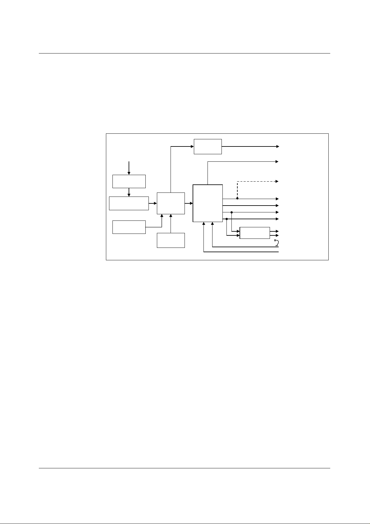
SYSTEM DIAGRAM
MEDIA
FRONT END
HOME
CONNECTIVITY
SYSTEM
CLOCKS
DIGITAL
DECODER
STORAGE
(HDD)
VIDEO
DAC
WM8722
AUDIO
DAC
L
R
L
R
AMPLIFIER
VIDEO OUT
TONE
GENERATOR
OUTPUT
MONO AUDIO
OUTPUT
(OPTIONAL)
VARIABLE LEVEL
AUDIO OUTPUT (TV)
LINE LEVEL AUD IO
OUTPUT (VCR)
HEADPHONE
OUT
MIC OR
ANALOGUE
INPUT
Figure 10. Digital Set Top Box Application
The WM8722 is a com plete audio sub-sys tem desi gned for digital set top box applications. A typic al
application might require audi o outputs to be routed to a VCR and television. The W M8722 allows
the user to control the output audio level being sent to t he television whilst m aintaining a constant
volume level to the VCR. The on-board t one generator can be programmed to provide a audible
warning signal from the set top box to the television outputs without appearing on the line level
outputs. The W M8722 can al so directly generate a mono signal for UHF outputs.
The WM8722 contains a stereo analogue input. This signal can be routed or m ixed together onto t he
line and variable outputs. It can be used to control the volume level of an audio output from another
audio source such as a games machine or additi onal set top box. Alternatively, it could be used to
provide a karaoke input from a digi tal effects processor.
WOLFSON MICROELECTRONICS LTD AI Rev 1.5 May 2000
21
Page 22
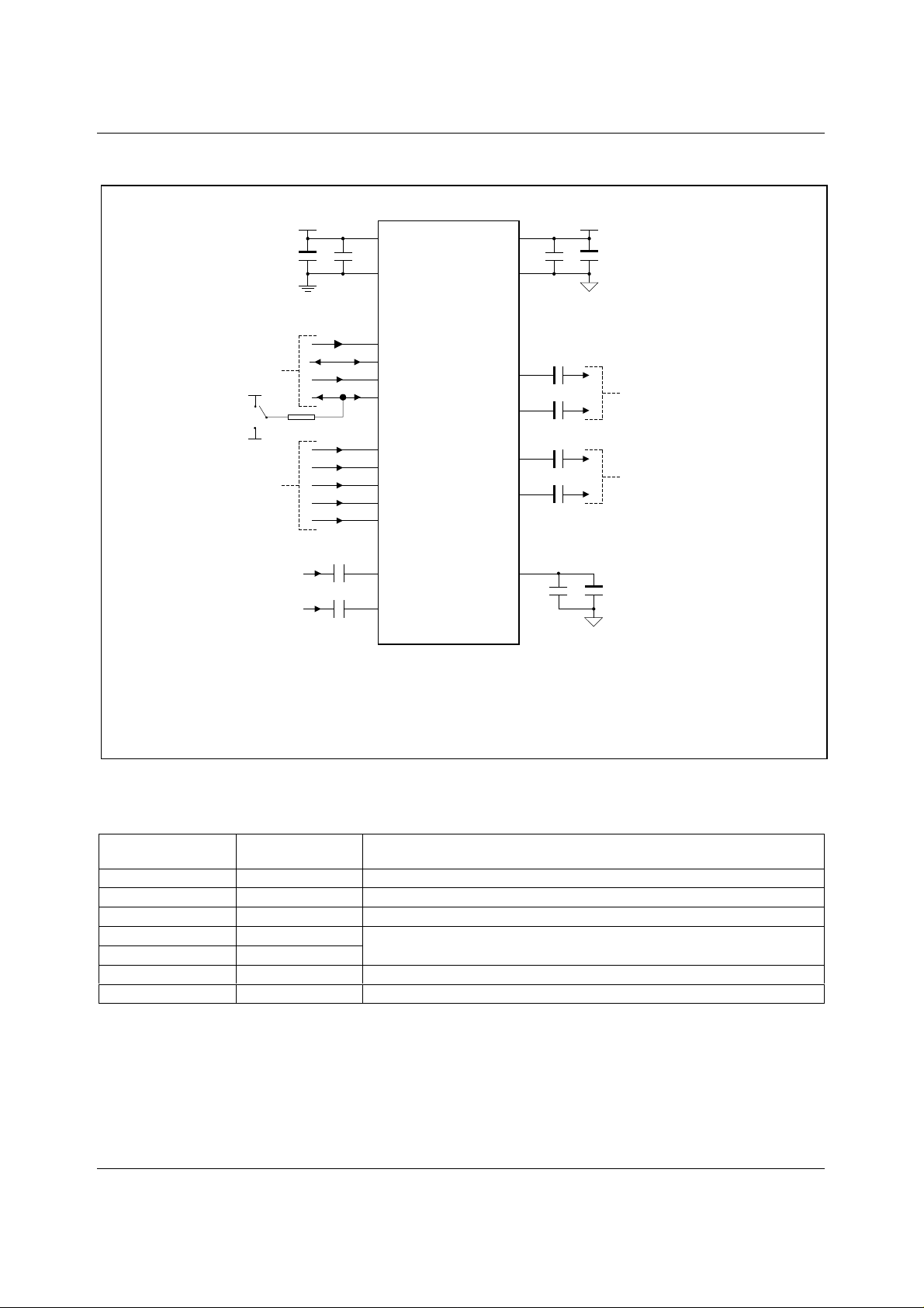
WM8722 Advanced Information RECOMMENDED EXTERNAL COMPONENTS
DVDD
+
C
1
DGND
SPI or 2-wire
3
Interface
2-wire Interface
SPI Interface
DVDD
R1
DGND
Audio Serial Data I/F
C
C
NOTES: 1. AGND and DGND should be connected as close to the WM8722 as possible.
2. C
, C3, C9, C10 and C11 should be positioned as close to the WM8722 as possible.
2
3. Capacitor types should be carefully chosen. Capacitors with very low ESR are
recommended for optimum performance.
6
DVDD
C
2
16
DGND
2
MC
MD
4
LATCH
5
BUSY
WM8722
1
TCLK
17
DIN
18
LRCIN
19
BCKIN
20
SCKI
9
7
MIXINR
10
14
MIXINL
AVDD
AGND
VAROUTR
VAROUTL
LINEOUTR
LINEOUTL
CAP
11
10
9
12
8
13
15
AVDD
C
3
C
+ + + +
C
C
7
+
C
4
AGND
5
AC-Coupled
6
Variable Outputs
to External LPF
AC-Coupled
C
8
C
C
12
11
AGND
Line Level outputs
to External LPF
+
Figure 11. External Components Diagram
RECOMMENDED EXTERNAL COMPONENTS VALUES
COMPONENT
REFERENCE
C1 and C4 10µF
C2 and C3 0. 1µF
C5, C6, C7 and C8 10µF
C11 0.1µF
C12 10µF
R1 10kΩ
C9,C10 1µF
Table 11. External Components Description
WOLFSON MICROELECTRONICS LTD AI Rev 1.5 May 2000
SUGGESTED
VALUE
DESCRIPTION
De-coupling for DVDD and AVDD.
De-coupling for DVDD and AVDD.
Output AC coupling caps t o remove midrail DC level from outputs.
Reference de-coupling capacit ors for CAP pin.
AC coupling capacitors for setting DC inputs level of anal ogue
22
Page 23
Advanced Information WM8722
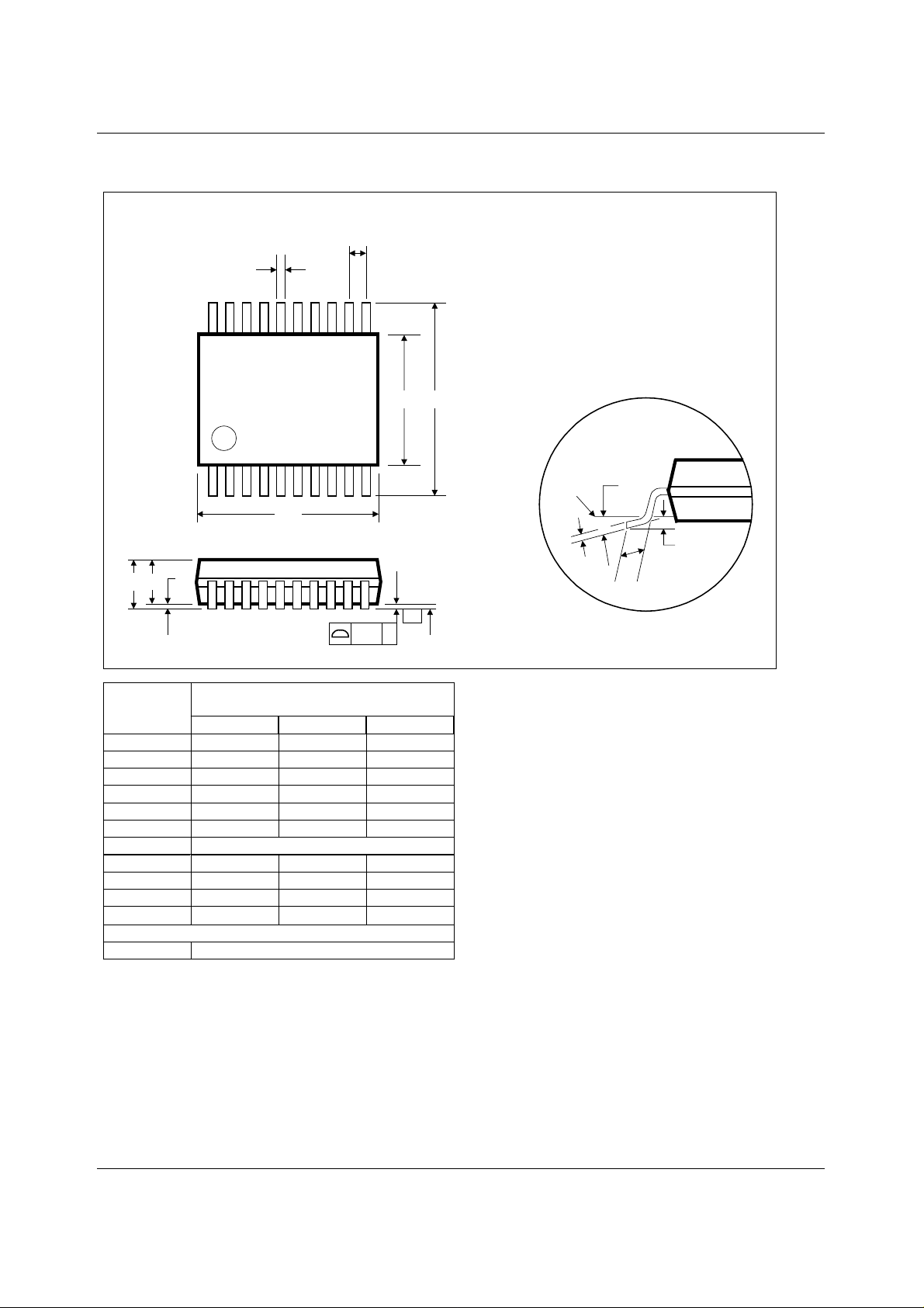
PACKAGE DIMENSIONS
DM0015.ADS: 20 PIN SSOP (7.2 x 5.3 x 1.75 mm)
A
A2
Symbols
A
A
1
A
2
b
c
D
e
E
E
1
L
θ
b
D
A1
Dimensions
(mm)
MIN NOM MAX
----- ----- 2.0
0.05 ----- -----
1.65 1.75 1.85
0.22 ----- 0.38
0.09 ----- 0.25
6.90 7.20 7.50
0.65 BSC
7.40 7.80 8.20
5.00 5.30 5.60
0.55 0.75 0.95
o
0
o
4
e
1120
101
0.10 C
E1 E
-C-
SEATING PLANE
o
8
GAUGE
PLANE
Θ
0.25
c
L
REF:
NOTES:
A. ALL LINEAR DIMENSIONS ARE IN MILLIMETERS.
B. THIS DRAWING IS SUBJECT TO CHANGE WITHOUT NOTICE.
C. BODY DIMENSIONS DO NOT INCLUDE MOLD FLASH OR PROTRUSION, NOT TO EXCEED 0.20MM.
D. MEETS JEDEC.95 MO-150, VARIATION = AE. REFER TO THIS SPECIFICATION FOR FURTHER DETAILS.
JEDEC.95, MO-150
WOLFSON MICROELECTRONICS LTD AI Rev 1.5 May 2000
23
 Loading...