

Page 1
WM8733
102dB Stereo DAC
Product Preview, July 2000, Rev 1.3
DESCRIPTION
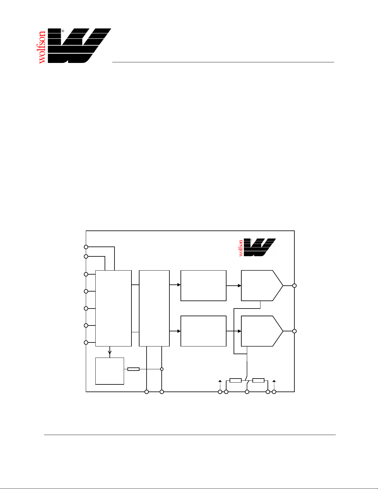
WM8733 is a high perform ance st ereo DAC designed f or use in
portable audio equipment, video CD players and similar
applications. It c omprises selectable normal or I
serial data interfaces for 16 to 24-bit input s, high performance
digital filters, and s igm a-del ta out put DACs , ac hieving an 102dB
signal-to-noise ratio.
The device is available in a 14-pin SOIC package that offers
selectable mute and de-em phas is func tions usi ng a m inim um of
external components.
Low supply voltage operation and low current c onsumption are
valuable features, particul arl y for use in portable equipment.
Additional modes consist of a powerdown option and the
possibility of generating separate differential left and right
outputs for applications demanding higher performance.
2
S compatible
BLOCK DIAGRAM
SEL[0]
SEL[1]
MODE
0
Normal stereo
1
Power down
0
Left only differential output
1
Right only differential output
SEL[0] (4)
SEL[1] (11)
0
0
1
1
FEATURES
• High tolerance to clock jitter
• Compatible with PCM 1733
• Distortion > 90dB, SNR > 102dB, dynamic range
performance > 100dB
• Stereo DAC with input sampling from 8kHz to 96kHz
• Additional mute feature and high performance
differential modes
• Normal or I
• Sigma-delta design with 64x oversamplin g
• System clock 256fs or 384fs or 512fs
• Supply range 3V to 5V
• Analogue voltage output to drive 2kΩ load
• 14-pin SOIC package
2
S compatible data format
APPLICATIONS
• High performance consumer audio
WM8733
FORMAT (13)
SCKI (14)
LRCIN (1)
SERIAL
INTERFACE
DIGITAL
FILTERS
DIN (2)
BCKIN (3)
INFINITE
ZERO
DETECT
10k
Wired
OR
(12)
DEEMPH
(10)
MUTE
WOLFSON MICROELECTRONICS LTD.
Lutton Court, Bernard Terrace, Edi nburgh, EH8 9NX, UK
Tel: +44 (0) 131 667 9386
Fax: +44 (0) 131 667 5176
Email: [email protected]
http://www.wolfson.co.uk
DIGITAL
SIGMA-DELTA
MODULATOR
DIGITAL
SIGMA-DELTA
MODULATOR
DIGITAL
VDD
SWITCHED
CAPACITOR
DAC
SWITCHED
CAPACITOR
DAC
DIGITAL
GND
(8)
VDD
(5)
CAP
specifications for products in the formative
phase of development. These products may
be changed or discontinued without notice.
(7)
GND
Product Preview data sheets contain
2000 Wolfson Microelectronics Ltd.
(6) VOUTR
(9) VOUTL
Page 2
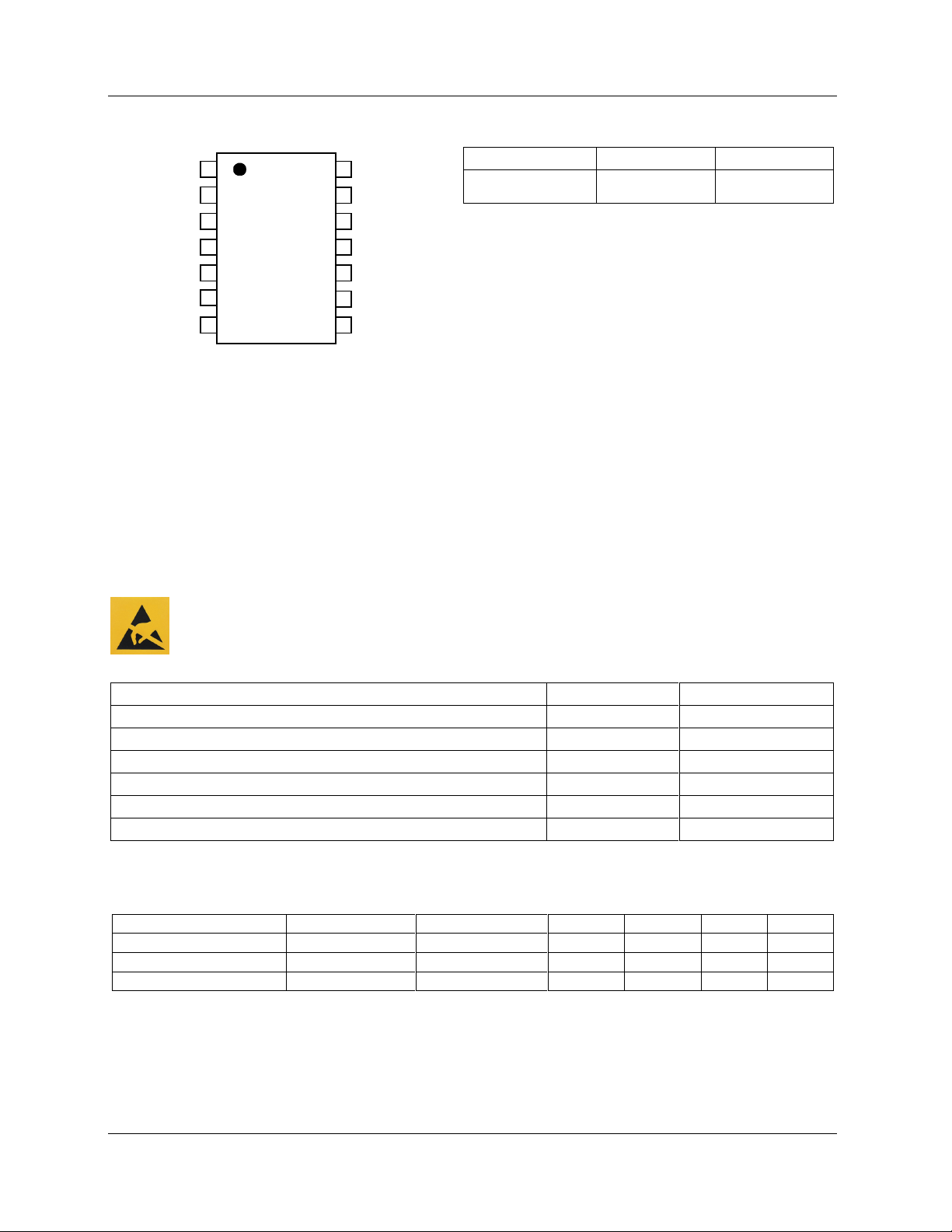
WM8733 Product Preview PIN CONFIGURATION
LRCIN
DIN
BCKIN
SEL0
CAP
VOUTR
GND
1
2
3
WM8733
4
5
6
7
14
13
12
11
10
9
8
SCKI
FORMAT
DEEMPH
SEL1
MUTE
VOUTL
VDD
ORDERING INFORMATION
DEVICE TEMP. RANGE PACKAGE
XWM8733ED -25 to +85oC 14-pin SOIC
ABSOLUTE MAXIMUM RATINGS
Absolute Maximum Ratings are stress rat ings only. Perm anent damage to the devic e may be caused by cont inuously operating
at or beyond these limits. Device functional operati ng limits and guaranteed performance spec i fications are given under Electrical
Characteristics at the test conditions s pecified
ESD Sensitive Device. This device is manufac tured on a CMOS proc ess . I t i s t herefore generic ally s usc epti ble
to damage from excessi ve static voltages. Proper ESD precautions must be taken during handling and s torage
of this device.
CONDITION MIN MAX
Supply voltage
Reference input
Operating temperature range, T
Storage temperature
Lead temperature (soldering, 10 s econds)
Lead temperature (soldering, 2 minutes)
A
-0.3V +7.0V
VDD+0.3V
+260
+183
o
C
o
C
o
C
-25oC+85
o
-65
C +150oC
RECOMMENDED OPERATING CONDITIONS
PARAMETER SYMBOL TEST CONDITIONS MIN TYP MAX UNIT
Supply range
Ground
Supply current
WOLFSON MICROELECTRONICS LTD PP Rev 1.3 July 2000
VDD -10% 3.0 to 5.0 +10% V
GND 0 V
VDD = 5V 15 mA
2
Page 3
Product Preview WM8733
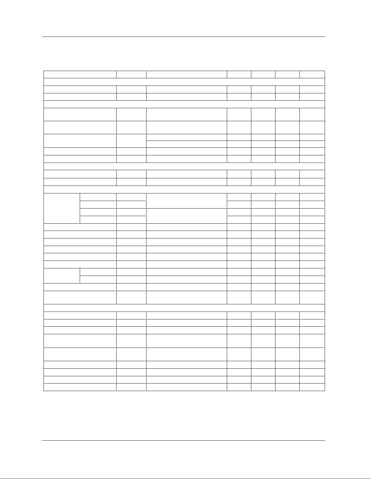
ELECTRICAL CHARACTERISTICS
Test Characteristics
VDD = 5V, GND = 0V, T
PARAMETER SYMBOL TEST CONDITIONS MIN TYP MAX UNIT
Digital Logic Levels
Input LOW level
Input HIGH level
Analogue Output Levels
Output level
Minimum resist ance load
Maximum capacitance load
Output DC level
Reference Levels
Potential divider resis tance
Voltage at CAP
DAC Circuit Specifications
SNR (Note 1) Stereo mode
Mono mode
Stereo mode
Mono mode
THD (full scale)
THD+N
Frequency response
Pass band ripple
Transition band
Out of band rejection
Dynamic
Range
Stereo mode
Mono mode
Channel Separation
Gain mismatch
channel-to-channel
Audio Data Input and System Clock Timing Information
BCKIN pulse cycle time
BCKIN pulse width high
BCKIN pulse width low
BCKIN rising edge to LRCIN
edge
LRCIN rising edge to BCKIN
rising edge
DIN setup time
DIN hold time
System clock pul se width high
System clock pul se width low
Note 1 Ratio of RMS output level with 1kHz full scale input, to t he RMS output level with al l zeros into t he digi tal i nput, m easured
“A” weighted over a 20Hz to 20kHz bandwidth.
Note 2 All performance measurem ents done with 20kHz low pass filter. Failure to use such a f ilter will result in higher THD+N
and lower SNR and Dynamic Range readings than are found in the Electric al Charact eris ti cs . The low pass fi lter rem oves
out of band noise; although it i s not audible it may affect dynamic specification values.
= +25oC, fs = 44.1kHz, SCKI = 384fs unless otherwise stated.
A
V
IL
V
IH
Into 10kohm, full scale 0dB,
(5V supply)
Into 10kohm, full scale 0dB,
(3V supply)
o midrail or AC coupled (5V s uppl y) 2 10 kohms
o midrail or AC coupled (3V s uppl y) 10 kohms
5V or 3V 100 pF
VDD to CAP and CAP to GND
VDD = 5V
VDD = 3V
0dB 0.03 0.01 %
-60dB -35 -40 dB
t
BCY
t
BCH
t
BCL
t
BL
t
LB
t
DS
t
DH
t
SCKIH
t
SCKIL
0.8 V
2.0 V
1V
0.6 V
RMS
RMS
VDD/2 V
80 100 120 kohms
VDD/2
98 102 dB
dB
96 100 dB
dB
0 20,000 Hz
±0.25 dB
20,000 Hz
-40 dB
100 dB
dB
90 dB
±1 ±5 %FSR
100 ns
50 ns
50 ns
30 ns
30 ns
30 ns
30 ns
13 ns
13 ns
WOLFSON MICROELECTRONICS LTD PP Rev 1.3 July 2000
3
Page 4

WM8733 Product Preview PIN DESCRIPTION
PIN NAME TYPE DESCRIPTION
1
2
3
4
5
6
7
8
9
10
11
12
13
14
LRCIN Digital input Sample rate clock input
DIN Digital input Serial data input
BCKIN Digital input Bit clock input
SEL0 Digital input Mode select (internal pull-down)
CAP Analogue output Analogue internal reference
VOUTR Analogue output Right channel DAC output
GND Supply 0V supply
VDD Supply Positive supply
VOUTL Analogue output Lef t channel DAC output
MUTE Digital input Soft mute control; high = muted, Z = aut o mute input/output
SEL1 Digital input Mode select (internal pull-down)
DEEMPH Digital input De-emphasis select; hi gh = de-emphasis ON (44.1kHz only), (internal
FORMAT Digital input Data input format select; ‘lo’ = normal, ‘hi’ = I
SCKI Digital input System clock input (256fs or 384fs or 512fs)
pull-up)
2
S (internal pull-up)
WOLFSON MICROELECTRONICS LTD PP Rev 1.3 July 2000
4
Page 5

Product Preview WM8733
DEVICE DESCRIPTION
INTRODUCTION
WM8733 is a com plete high perform ance stereo audio 18-bi t digital-to-anal ogue converter, inc luding
digital interpolation fil ter, mult ibit sigm a-delta with dither, and switched capac itor mult ibit stereo DA C
and output smoothing fil ters.
Special functions of soft mute and de-emphas is are provided, and operation using system clock of
256fs, or 384fs or 512fs is provided, selection between either clock rate being automatically
controlled. Sample rat es (fs) from less than 8ks/ s to 96ks/s are allowed, provided the appropriate
system clock is input.
An auto mute function is provided which is enabled if MUTE (pin 10) is lef t at high impedanc e. If 64
successive left and right channel data samples of value 0 are received, auto m ute is achieved. This
signal is wire ORed to MUTE (pin 10) via 10K resist or. If MUTE (pin 10) internally is not externally
driven, the internal auto mute state is visible on this pin as a weak drive strength signal (10kΩ
source).
MUTE DESCRIPTION
0
Z
1
Table 1 Soft Mute Control
A novel multi bit sigma-delta DAC design is used, utilising a 64x oversampling rate, to optimise
signal to noise performance and offer increased clock jitter tolerance.
Internally generated midrail references are us ed to DC bias output signals, requiring only a singl e
external capacitor for decoupling purposes.
The device is packaged in a small 14-pin SOIC package, offering pin compatibility with Burr Brown
PCM1733, but with added functionality of a soft mut e input pin, which may be left float ing to enable
auto mute detection, or hel d ‘low’ leaving the device operational.
Single 3V to 5V supplies may be used, the output ampli tude scaling with absolut e supply level. Low
supply voltage operation and low current consum ption, and the low pin count sm all package, make
the WM8733 attract i ve for many consumer type appli cations.
Soft mute is OFF
Auto mute is enabled
Soft mute is ON
WOLFSON MICROELECTRONICS LTD PP Rev 1.3 July 2000
5
Page 6

WM8733 Product Preview
DAC CIRCUITS
The WM8733 DACs are designed t o allow playback of 18-bit PCM audio or s imilar data with high
resolution and low noise and distortion. Sample rates up to 96ks/s may be used, with m uch lower
sample rates acc eptable provided that the ratio of sample rate (LRCIN) to system clock is m ai ntained
at the required 256fs, or 384fs or 512f s times.
The DACs on WM8733 are implemented using sigma-delta oversampled conversion techniques.
These require that the PCM samples are digitally filtered and interpolated to generate a set of
samples at a much higher rate than the input rate. This sam ple stream is then digit ally modulated t o
generate a digital pulse stream that is then converted to analogue s ignals in a switched capacitor
DAC. The advantage of this tec hnique is that t he DAC is linearis ed using noise shapi ng techniques ,
allowing the 16-bit resolution to be m et using non-c ritic al analogue com ponents . A furt her advantage
is that the high sam ple rate at the DA C output m eans t hat s m oothi ng fil ters on the out put of t he DAC
need only have fairly crude characteris tics in order to remove the c haracteri stic st eps, or im ages, on
the output of the DAC. In order to ensure that generation of tones characteristic to sigma-delta
convertors is not a problem , dithering is used in the digital modulator, and a higher order modul ator is
used. The switched capacitor technique used in the DAC reduces s ensitivit y to clock jitter com pared
to switched current techniques used in other implementations.
De-emphasis of 44.1kHz signals may be applied if requi red.
DEEMPH DESCRIPTION
0 De-emphasis is OFF
1 De-emphasis is ON
Table 2 De-emphasis Control
(44.1kHz only)
The voltage on the CAP pin is used as the reference for the DACs, therefore t he amplitude of the
signals at the DAC outputs will scale with the amplitude of the voltage at the CAP. An external
reference could be used to drive in on the CAP pin if desired, but a value typically of about midrai l
should be used for optimum performance.
The outputs of the 2 DACs are buff ered out of the device by buffer amplifiers. These amplif iers will
source load current of several m A and sink current up to 1.5m A, so allowing signif icant loads to be
driven. The output source is ac tive, the sink is Class A, i.e. fixed value, so greater loads m ight be
driven if an external ‘pull-down’ resistor is connected at the output.
Typically an external low pass filter circuit will be used to remove residual sampling nois e of the 64x
oversampling used and if des i red adj ust the signal amplit ude and devi ce strength.
WOLFSON MICROELECTRONICS LTD PP Rev 1.3 July 2000
6
Page 7
Product Preview WM8733
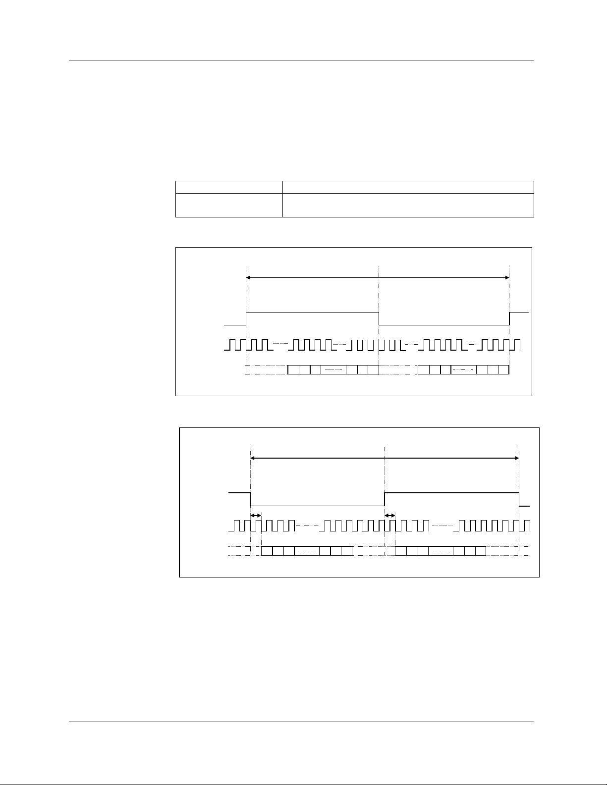
SERIAL DATA INTERFACE
WM8733 has serial int erface formats that are fully compat ible with both normal (MSB first, rightjustified) and I
LOW, normal data format is selected. When the f ormat is HIGH, I
If the application dem ands 16-bit or 20-bit dat a, then I
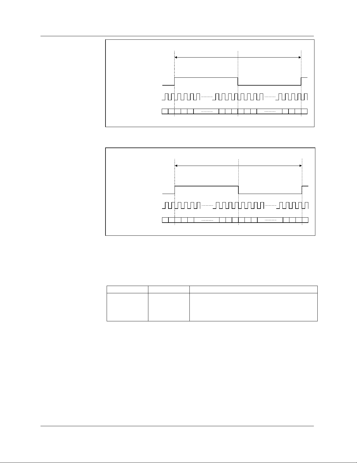
in 20-bit mode. Normal mode will support 18-bit data applicat ions or 16-bit pac ked m ode applic ations
(automatically detec ted).
Note: In 16-bit “packed” mode operation (exactly 32 BLCKS per LRCIN period) the data word must
align exactly with LRCIN clock edges (effectively both left and ri ght justified at the same time).
Table 3 Serial Interface Formats
2
S interfaces. The data form at is selected with the FORMAT pin. When FORMAT is
2
S format may be used. Two LSBs will be lost
2
S format is sel ected.
FORMAT DESCRIPTION
0
1
LRCIN
Normal format (MSB-first, right justi fied)
2
S format (Philips serial data protocol)
I
1/fs
LEFT CHANNEL RIGHT CHANNEL
BCKIN
DIN
AUDIO DATA WORD = 18-BIT
1 2 3 161718 1 2 3 16 17 18
MSB MSB LSB
Figure 1 ‘Normal’ Data Input Timing
LEFT CHANNEL RIGHT CHANNEL
LRCIN
BCKIN
DIN
AUDIO DATA WORD = 18-BIT
123 1617
MSB MSB LSBLSB
Figure 2 I2S Data Input Timing
LSB
1/fs
18
123 1617
18
WOLFSON MICROELECTRONICS LTD PP Rev 1.3 July 2000
7
Page 8
WM8733 Product Preview
1/fs
LEFT CHANNEL RIGHT CHANNEL
LRCIN
BCKIN
MODE SELECT PINS
DIN
AUDIO DATA WORD = 16-BIT
MSB MSB LSBLSB
Figure 3 16-bit Normal Packed Mode
LRCIN
BCKIN
DIN
AUDIO DATA WORD = 18-BIT
MSB MSB LSBLSB
Figure 4 18-bit Normal Packed Mode
The WM8733 has four possi bl e modes.
14 15 16123 114 15 1612315 16
1/fs
LEFT CHANNEL RIGHT CHANNEL
16 17 18123 116 17 1812317 18
SEL0 SEL1 MODE
0
0
1
1
0
1
0
1
Normal stereo operation
Power down
Left only differential out put
Right only differential output
Table 4 Mode Select Pins
The SEL0/1 pins (pins 4 and 11) can be hard wired, or left floating as internal “pull-downs” will cause
the device to operate in normal stereo mode.
WOLFSON MICROELECTRONICS LTD PP Rev 1.3 July 2000
8
Page 9
Product Preview WM8733
SYSTEM CLOCK
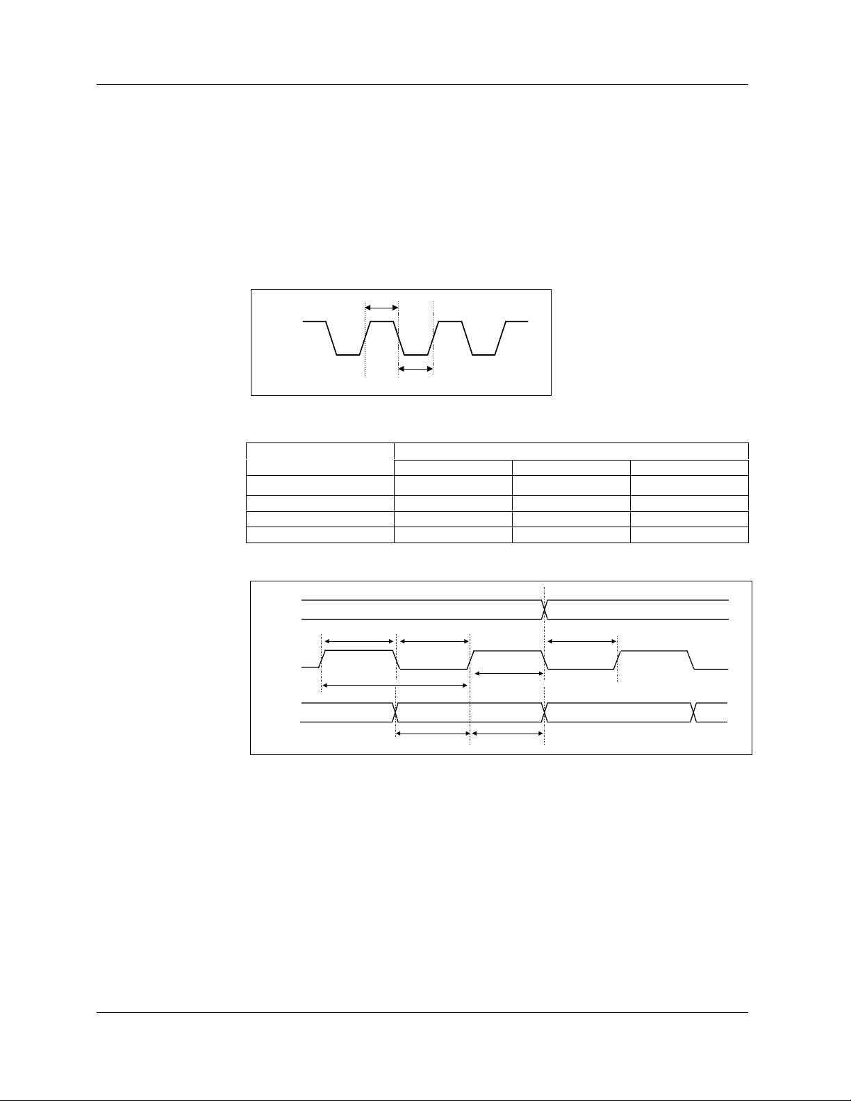
The system clock is used to operate the digital filters and the noise shaping circuits . The system
clock input is at pi n 14 (SCKI). The frequency of WM8733’s syst em clock s hould be set to 256fs or
384fs or 512fs, (where fs is the audio sam pli ng frequenc y). The s am ple rate i s t ypical ly: 32 k Hz, 44. 1
kHz, 48 kHz or 96kHz.
WM8733 has a system clock detection circuit that automatically determines whether the system
clock being supplied is at 256fs or 384fs or 512fs. The system cl ock should be s ynchronised with
LRCIN, but WM8733 is tolerant of phase differences. Severe distortion in the phase difference
between LRCIN and the system clock will be detected, and cause the device to automatically
resynchronise. During resynchronisation, the output of the device will either repeat the previous
sample, or drop the next sample, depending on the nat ure of the phase slip. This will ensure minim al
“click“ at the analog outputs during resync hroni sation.
t
SCKIH
SCKI
t
SCKIL
Figure 5 System Clock Timing Requirements
SAMPLING RATE
(LRCIN)
SYSTEM CLOCK FREQUENCY (MHz)
256fs 384fs 512fs
32 kHz 8.192 12.288 16.384
44.1 kHz 11.2896 16.9340 22.5792
48 kHz 12.288 18.432 24.576
96kHz 24.576 36.864 49.152
Table 5 System Clock Frequencies Versus Sampling Rate
LRCIN
t
BCL
t
BL
t
DS
t
DH
BCKIN
DIN
t
BCH
t
BCY
Figure 6 Audio Data Input Timing
t
LB
WOLFSON MICROELECTRONICS LTD PP Rev 1.3 July 2000
9
Page 10
WM8733 Product Preview RECOMMENDED EXTERNAL COMPONENTS
FROM AUDIO
PROCESSOR
ANALOGUE
OUTPUT FOR
RIGHT
CHANNEL
GND
VDD
10µF
External
LPF
10µF
0.1µF
1
LRCIN
2
DIN
3
BCKIN
SEL0
CAP
VOUTR
GND
WM8733
4
+
5
6
7
SCKI
FORMAT
DEEMPH
SEL1
MUTE
VOUTL
VDD
14
13
12
11
(diode allows automute operation)
10
9
8
External
LPF
256fs/384fs/512fs CLK
ANALOGUE
OUTPUT FOR
LEFT CHANNEL
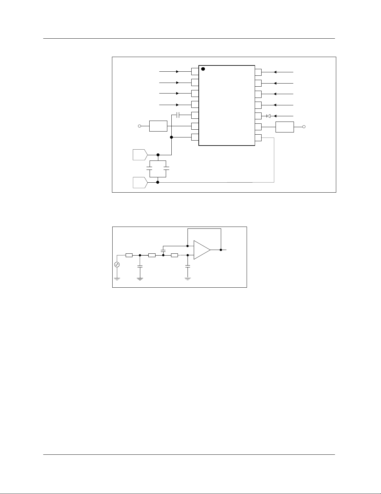
Figure 5 Applications Diagram
DETAIL OF APPLICATION DIAGRAM SHOWING THE EXTERNAL LOW POWER FILTER
External LPF
x2 for Stereo Operation
1500pF
10k
680pF
Ω
10k
10k
Ω
+
Vin
-
-
+
Ω
100pF
Filtered
Analogue
Output
Figure 6 Third-Order Low Pass Filter (LPF) Example
An external low pass filter is recom m ended i f t he device i s dri ving a wide band ampl ifi er, as shown in
Figure 6. In some applications, second-order or passive RC filter may be adequate.
WOLFSON MICROELECTRONICS LTD PP Rev 1.3 July 2000
10
Page 11
Product Preview WM8733
PACKAGE DIMENSIONS
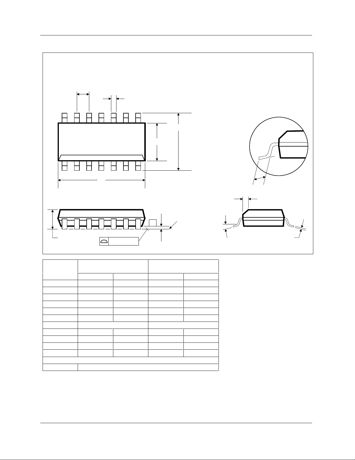
D: 14 PIN SOIC 3.9mm Wide Body
e
14
D
B
DM001.C
8
H
E
71
L
o
h x 45
A1
-C-
SEATING PLANE
α
A
Symbols
0.10 (0.004)
Dimensions
(MM)
Dimensions
(Inches)
MIN MAX MIN MAX
A
A1
B
C
D
E
e
H
h
L
α
REF:
NOTES:
A. ALL LINEAR DIMENSIONS ARE IN MILLIMETERS (INCHES).
B. THIS DRAWING IS SUBJECT TO CHANGE WITHOUT NOTICE.
C. BODY DIMENSIONS DO NOT INCLUDE MOLD FLASH OR PROTRUSION, NOT TO EXCEED 0.25MM (0.010IN).
D. MEETS JEDEC.95 MS-012, VARIATION = AB. REFER TO THIS SPECIFICATION FOR FURTHER DETAILS.
1.35 1.75 0.0532 0.0688
0.10 0.25 0.0040 0.0098
0.33 0.51 0.0130 0.0200
0.19 0.25 0.0075 0.0098
8.55 8.75 0.3367 0.3444
3.80 4.00 0.1497 0.1574
1.27 BSC 0.05 B SC
5.80 6.20 0.2284 0.2440
0.25 0.50 0.0099 0.0196
0.40 1.27 0.0160 0.0500
o
0
o
8
o
0
8
JEDEC.95, MS-012
o
C
WOLFSON MICROELECTRONICS LTD PP Rev 1.3 July 2000
11
 Loading...