

Page 1
WM8816
Stereo Digital Volume Control
Advanced Information, September 2000, Rev 1.1
DESCRIPTION
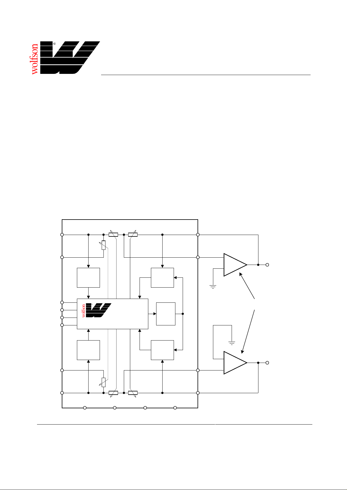
The WM8816 is a highly linear stereo volume control for
audio systems. The des ign is based on resist or chains with
external op-amps, which provides flexibility for the supply
voltage, signal swing, noise f loor and cos t opt imi sation. The
gain of each channel can be independently programmed
from -111.5dB to +15.5dB through a digital serial control
interface.
Audible clicks on gain changes are eliminated by changing
gains only when a zero crossing has been det ected in the
signal. The device also feat ures peak level detec tion, which
can be used for Automatic Gain Control. The WM8816
operates from a single +5V supply and accepts signal input
levels up to ±18V.
The WM8816 is available in a 16-pin SOIC package. It is
guaranteed over a temperature range of -40° to 85°C.
BLOCK DIAGRAM
LIN (4)
LGND (5)
Zero
Crossing
Detector
Peak
Level
Detector
FEATURES
• Gain range from -111.5dB to +15.5dB
• 0.5dB Gain step size
• Total Harmonic Distortion 0.001% (100dB) typical
• Crosstalk -110dB typic al
• Input signals up to ±18V
• Zero Detection for Gain Changes
• Hardware and Software Mute
• Power On/Off Transient Suppression
APPLICATIONS
• Audio Amplifiers
• Consumer Audio / Entert ai nment Systems
• Mixing Desks
• Audio Recording Equipment
(3) LFO
(2) LMO
-
+
LEFT OUT
CSB (6)
MUTEB (8)
DATA (9)
CCLK (10)
RGND (12)
RIN (13)
WM8816
Zero
Crossing
Detector
(1)
AVDD
(16)
AGND
Control
(7)
DVDD
WOLFSON MICROELECTRONICS LTD
Lutton Court, Bernard Terrace, Edi nburgh, EH8 9NX, UK
Tel: +44 (0) 131 667 9386
Fax: +44 (0) 131 667 5176
Email: [email protected]
http://www.wolfson.co.uk
DAC
Peak
Level
Detector
(11)
DGND
External Opamps
+
(15) RMO
(14) RFO
-
Advanced information data sheets contain
preliminary data on new products in t he
pre-production phase of development .
Supplementary data will be published at a
2000 Wolfson Microelectronics Ltd.
RIGHT OUT
later date.
Page 2
WM8816 Advanced Information
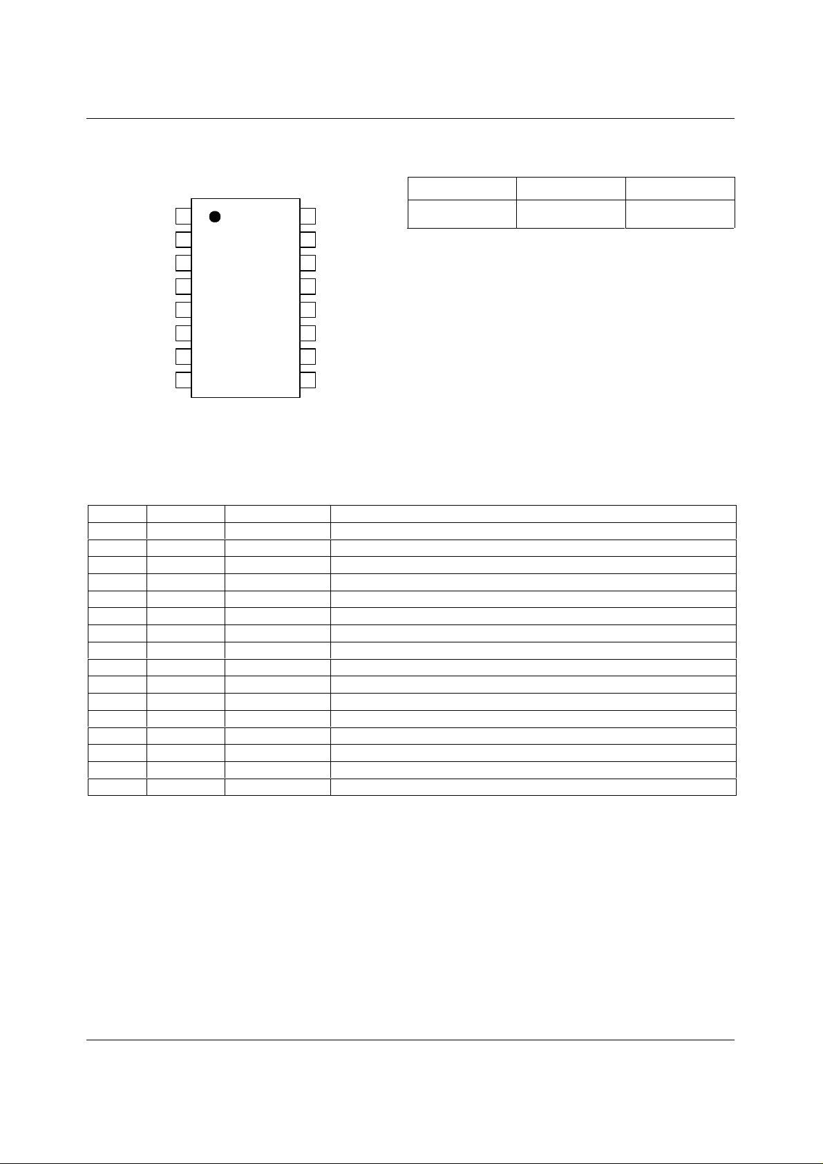
PIN CONFIGURATION ORDERING INFORMATION
DEVICE TEMP. RANGE PACKAGE
AVDD
LMO
LFO
LIN
LGND
CSB
DVDD
MUTEB
1
2
3
4
5
6
7
8
16
15
14
13
11
10
12
AGND
RMO
RFO
RIN
RGND
DGND
CCLK
DATA
9
PIN DESCRIPTION
PIN NAME TYPE DESCRIPTION
1
2
3
4
5
6
7
8
9
10
11
12
13
14
15
16
AVDD Supply Supply Voltage for Analogue Circuitry
LMO Analogue Output External Op-amp Inverting Input (Left Channel)
LFO Analogue Input External Op-amp Feedback Signal (Left Channel )
LIN Analogue Input Input Signal (Left Channel)
LGND A nal ogue Input Input Signal Ground (Left Channel)
CSB Digital Input Chip Select (active low)
DVDD Supply Supply Voltage for Digi tal Circuitry
MUTEB Digital Input Mute (active low)
DATA Digital In / Out Serial Interface Data Input / Output (tri-state)
CCLK Digital Input Serial Interfac e Cl ock
DGND Supply Digital Ground
RGND Analogue Input Input Signal Ground (Right Channel)
RIN Analogue Input Input Signal (Right Channel)
RFO Analogue Input External Op-amp Feedback Signal (Right Channel )
RMO Analogue Output External Op-amp Inverting Input (Right Channel )
AGND Supply Analogue Ground
XWM8816EDW -40 to +85oC 16-pin SOIC (plastic)
WOLFSON MICROELECTRONICS LTD AI Rev 1.1 September 2000
2
Page 3
Advanced Information WM8816
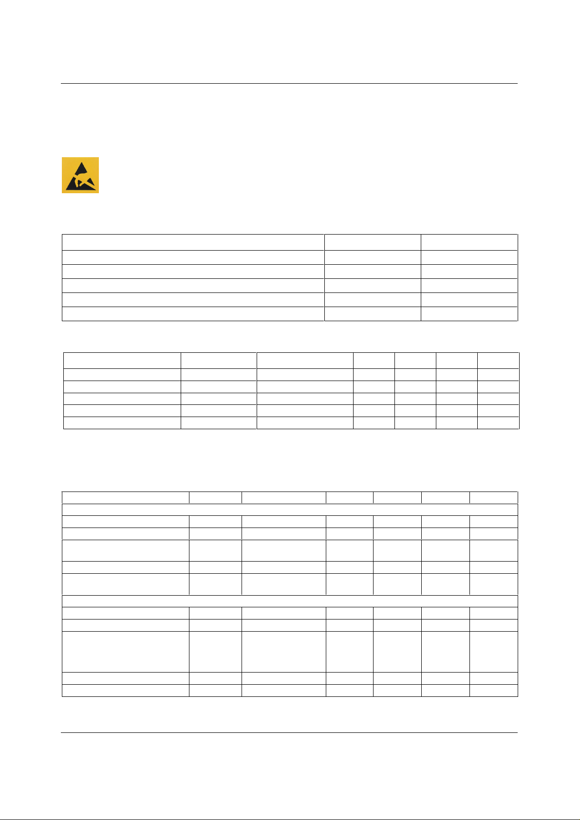
ABSOLUTE MAXIMUM RATINGS
Absolute Maximum Ratings are stress rati ngs only. Permanent damage to the devic e may be caused by cont inuously operating
at or beyond these limits. Devic e func tional operating l im it s and guarant eed perform anc e s pecif ic ati ons are given under E lec tr ical
Characteristics at the test conditions s pecified.
ESD Sensitive Device. Thi s device is manufactured on a CMOS process. It is therefore susceptible to damage
from excessive static voltages. To optimise the distortion and nois e performance of pins 3, 4, 13 and 14, the
on-chip ESD protection circuitry has been restrict ed, and cons equently only achi eves 300V when charact erised
to the Human Body Model. Proper ESD precautions must be taken during handling and storage of this devi ce.
As per JEDEC specification JES D22-A112-A, this product requires spec ific storage c onditions prior to surf ace m ount assem bly. I t
has been classified as havi ng a Moisture Sensitivity Level of 3 and i s therefore supplied in vacuum -sealed moisture barrier bags.
CONDITION MIN MAX
Input signal voltage
Positive supply volt age (AVDD to AGND, DVDD to DGND)
Input voltage (all other pins)
Operating temperature
Storage temperature
-20V +20V
-0.5V 6V
-0.5V AVDD + 0.5V
-40°C85°C
-55°C 125°C
RECOMMENDED OPERATING CONDITIONS
PARAMETER SYMBOL TES T CONDI TIONS MIN TYP MAX UNIT
Input signal voltage
Positive supply volt age
Negative supply voltage
Input signal grounds
Operating temperature
AVDD, DVDD 4.5 5 5.5 V
AGND, DGND 0 V
LGND, RGND 0 V
-18 +18 V
-20 60 60 °C
ELECTRICAL CHARACTERISTICS
TEST CONDITIONS
AVDD = 5.0V, AGND = 0V, T
PARAMETER SYMBOL TEST CONDITIONS MIN TYP MAX UNIT
Analogue Inputs / Outputs
Input resistance
Input capacitance
Input offset voltage
Supply current
Power supply rejection ratio
(Note 1)
Gain Control
Gain range G
Gain step size D
Gain error (Note 1) DE
Gain match error (Note 1) ME
Mute attenuation MATT
= 25°C, unless otherwise stat ed.
A
V
R
C
offset
IN
IN
For any gain 7 10 kΩ
For any gain 2 pF
External OP275
opamp, gain = 1
I
DD
From AVDD / AGND 2.5 5 mA
PSRR From AVDD 80 dB
Lowest gains
guaranteed by
design, not tested in
production.
Between channels 0.2 dB
1mV
-111.5 +15.5 dB
0.5 dB
0.5 dB
113 dB
WOLFSON MICROELECTRONICS LTD AI Rev 1.1 September 2000
3
Page 4

WM8816 Advanced Information
TEST CONDITIONS
AVDD = 5.0V, AGND = 0V, T
PARAMETER SYMBOL TEST CONDITIONS MIN TYP MAX UNIT
Audio Performance
Noise (Note 1)
V
= 0V, V
IN
with OP275,
OUT
A-weighed
Total Harmonic Distortion plus
Noise
Dynamic Range (Note 1)
Crosstalk (Note 1)
Digital Inputs / Outputs
Input low voltage V
Input high voltage V
Output low voltage V
Output high voltage V
Control Interface Timing
Clock Frequency
Period of CCLK high
Period of CCLK low
Rise time of CCLK
Fall time of CCLK
Hold time, CCLK high to CSB low
Setup time, CSB low to CCLK
high
Setup time, valid DATA to CCLK
high
Hold time, CCLK high to invalid
DATA
Setup time, CCLK low to valid
DATA
Hold time, CSB high or 16
CCLK low to invalid DATA
Hold time, 16th CCLK high to
CSB high
Setup time, CSB hi gh to CCLK
high
Note:
1. Guaranteed by design.
= 25°C, unless otherwise stat ed.
A
N Gain = -60dB 4 µV rms
V
IN
THD+N
DR 120 130 dB
CR Between channels ,
gain=0dB, f
IL
IH
OL
OH
f
CCLK
t
WHC
t
WLC
t
RC
t
FC
t
HCHS
t
SSLCH
t
SDCH
t
HCHD
t
DCLD
th
t
DSZ
t
HLCHS
t
SSHCH
Gain = 0dB 13
Gain = mute 2.5
= 1Vrms, gain=0dB,
V
with OP275,
OUT
DC to 20 kHz
0.001
(100)
-100 -110 dB
=1kHz
IN
All digital inputs 0.3 DVDD V
All digital inputs 0.7 DVDD V
I
= 2mA 0.4 V
Load
I
Load
= 2mA
DVDD -0.4 V
1MHz
VIH to V
VIL to V
VIL to V
VIH to V
IH
IL
IH
IL
500 ns
500 ns
100 ns
100 ns
20 ns
100 ns
100 ns
100 ns
Load = 100pF 200 ns
Load = 3.3kΩ 20 200 ns
200 ns
200 ns
%
(dB)
WOLFSON MICROELECTRONICS LTD AI Rev 1.1 September 2000
4
Page 5
Advanced Information WM8816
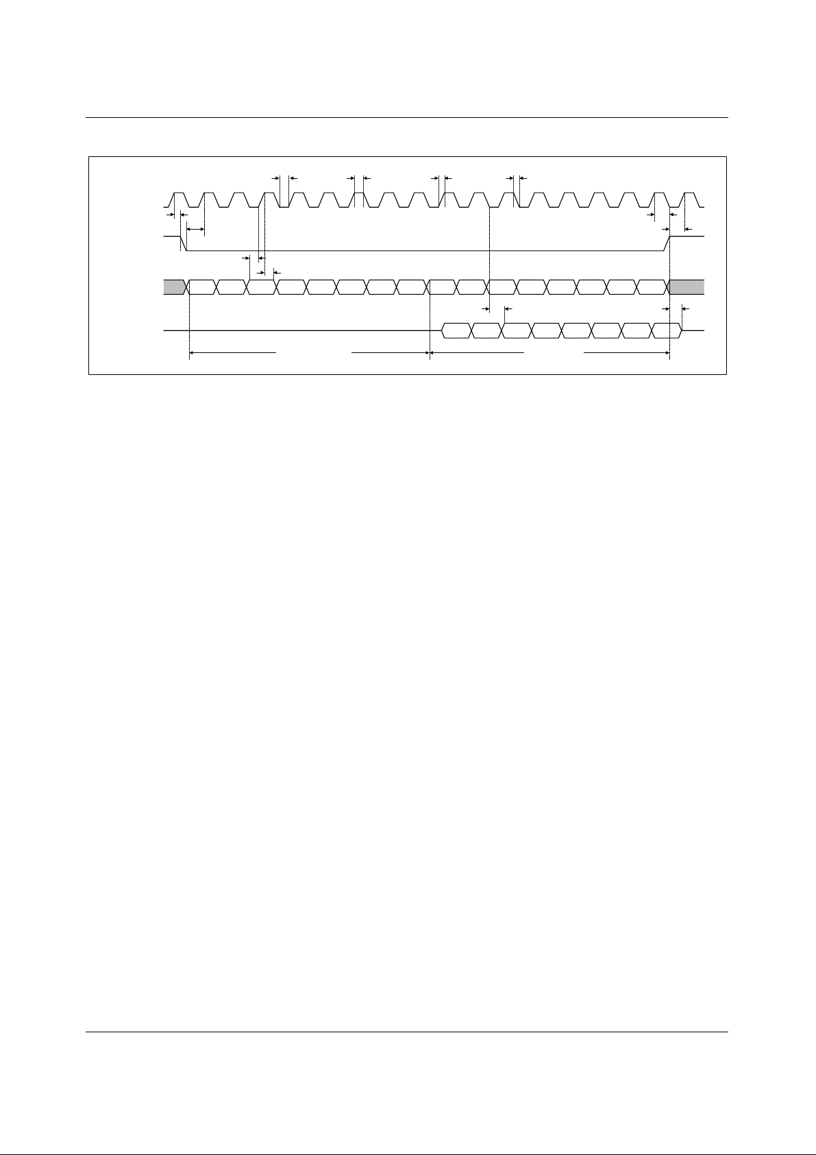
CONTROL INTERFACE TIMING DIAGRAM
CCLK
t
HCSH
t
SSLCH
CSB
t
SDCH
t
HCHD
A7DATA (IN) A6 A5 A4 A3 A2 A1 A0
DATA (OUT)
ADDRESS BYTE DATA BYTE
Figure 1 Control Interface Timing Diagram
t
WLC
t
WHC
t
RC
D7
D6 D5 D4 D3 D2 D1 D0
t
DCLD
t
FC
t
HLCHS
t
DSSHCH
t
DSZ
D7 D6 D5 D4 D3 D2 D1 D0
WOLFSON MICROELECTRONICS LTD AI Rev 1.1 September 2000
5
Page 6

WM8816 Advanced Information DEVICE DESCRIPTION
The WM8816 is a stereo digi tal volume control designed for audio systems. The levels of the left
and right analogue channels can be programm ed independently through the serial interface. The
resistor values in the internal resistor chains are decoded to 0.5 dB resolution with multiplexers,
giving a gain range of -111.5 to +15.5 dB. The code for -112 dB activates mute for maximum
attenuation.
The WM8816 has two constant impedance signal inputs. The lef t channel input is between LIN and
LGND, and the right channel between RIN and RGND. The output pi ns LFO, LMO (left) and RFO,
RMO (right) are designed to interface directly to two external op-amps, which produce the volum e
controlled output signals. This provides f lexibility for the supply voltage and signal swing; while the
WM8816 runs at 5V, t he output signal swing depends solely on the op-amp supply.
INTERFACES
Control information is written into or read back from the int ernal register via the serial control port.
This port consists of a bi-directional data pin (DATA), an acti ve low chip select pin (CSB) and the
control clock (CCLK). Control dat a is shi ft ed into t he seri al input regis ter on t he risi ng edges of CCLK
pulses, while CSB is low. All control instructions require two bytes of data. The first byte contains a 4bit register address and a read/write bit, and the second byte i s the c ontrol word. CSB m ust return to
high at the end of each word. W hen reading from the control registers , data is shifted out on the
falling edges of CCLK.
When CSB is high, the DATA pin is i n a high impedance s tate. In a m ulti-channel system , the sam e
DATA and CCLK lines can thus be connected to several WM8816 volume controllers, and each
device can be independently addressed by pulling its CSB pin low.
OPERATING MODES
When power is first applied, a power-on reset initialises t he control regist ers mutes the W M8816. To
activate the device, the MUTEB pin must be high and a non-zero value must be writt en to the gain
register. After that the device c an be muted again either by pulling the MUTEB pin low or by writing
zero (00hex) to the gain register.
For device testing, the MUTEB pin becomes an output when Bit 1 of the tes t regist er is high. Internal
signals can then be directed to MUTEB and monitored.
CHANGING THE GAIN OF THE CHANNEL
The WM8816 has two gain registers f or the left and right channels respectively. There is also an al i as
register address to update both gai n registers si multaneous ly. W hen a new gain value is written into
a gain register the WM8816 will wait until the next falling edge zero crossing in the input signal bef ore
changing the gain. This ensures that no audible click is produced at the output. If there are no zero
crossings in the si gnal aft er 18m s, the gai n is c hanged regardles s. If both gain regi st ers are changed
simultaneously, t he gai n i s changed first on the right and t hen the left channel.
PEAK LEVEL DETECTION
The WM8816 has an on-chip 8-bit di gital-to-analogue converter (DA C) used for monitori ng the peak
level of the output signal. The DAC input value i s program med via t he serial int erface. The reference
value V
peak signal level exceeds this value, the peak detector sets Bit 1 (for t he left channel) or Bi t 0 (right
channel) of the status register. These bits remai n set until the status regi ster is read.
is calculated from V
REF
= k/256 × 18V, where k is the DAC input code. When a positive
REF
WOLFSON MICROELECTRONICS LTD AI Rev 1.1 September 2000
6
Page 7

Advanced Information WM8816
REGISTER MAP
ADDRESS BYTE BITS DATA BYTEREGISTER
7 6 5 4 3 2 1 0 MSB…LSB Function
Peak Detector Status
CR4
Peak Detector
Reference
CR3
Left Channel Gain
CR2
Right Channel Gain
CR1
Test, CR5
Both Channel Gains
Table 1 Register Map Description
X 1 0 1 1 R/W X X Output code
00000000
00000001
00000010
00000011
X 1 1 0 0 R/W X X Input code
11111111
11111110
11111101
:
00000010
00000001
00000000
X 1 1 0 1 R/W X X Input code
11111111
11111110
11111101
:
11100000
00000010
00000001
00000000
X 1 1 1 0 R/W X X Input code
11111111
11111110
11111101
:
11100000
00000010
00000001
00000000
X1111R/WXX Reserved
X 1 0 0 1 W X X Write to both gai n regi sters
No overload
Right overload
Left overload
Both overload
DAC output
255/256 × 18V
254/256 × 18V
253/256 × 18V
2/256 × 18V
1/256 × 18V
AGND
Gain dB
+15.5
+15.0
+14.5
-111.0
-111.5
mute
Gain dB
+15.5
+15.0
+14.5
-111.0
-111.5
mute
:
:
0.0
:
0.0
Notes:
1. Address bit 2 is the read / write bit (1 for read, 0 for write).
2. X are don’t cares, set to 1 for m i ni mum power consumption.
3. All registers are set to their default value (all zeros) during power-on reset, except CR3 which is set to 255.
WOLFSON MICROELECTRONICS LTD AI Rev 1.1 September 2000
7
Page 8
WM8816 Advanced Information
TEST REGISTER
When bit 1 in register CR5 is set, MUTEB becomes an output pin. Bits 2, 3 and 4 select different
internal signals which can then be seen via the MUTEB pin.
CONDITION
76543210
Normal (MUTEB
0 0 0 0 0 0 0 1 Latc h the new gain value to resistor network
configured as input)
0 0 0 0 0 0 1 0 Left delay generator
0 0 0 0 0 1 1 0 Left peak detector
Test Mode
00001010 Left zero crossing
0 0 0 0 1 1 1 0 Left enable for zero crossing and delay generator
(MUTEB configured
as output)
0 0 0 1 0 0 1 0 Right delay generator
0 0 0 1 0 1 1 0 Right peak detector
00011010 Right zero crossing
0 0 0 1 1 1 1 0 Right enable for zero crossing and delay generator
Table 2 Test Register Description
PERFORMANCE GRAPHS
-70
-80
-90
THD+N
(dB)
-100
DATA BYTE BITS
FUNCTION
-110
-120
-60 +10-50 -40 -30 -20 -10 +0
Input Signal Level (dBV)
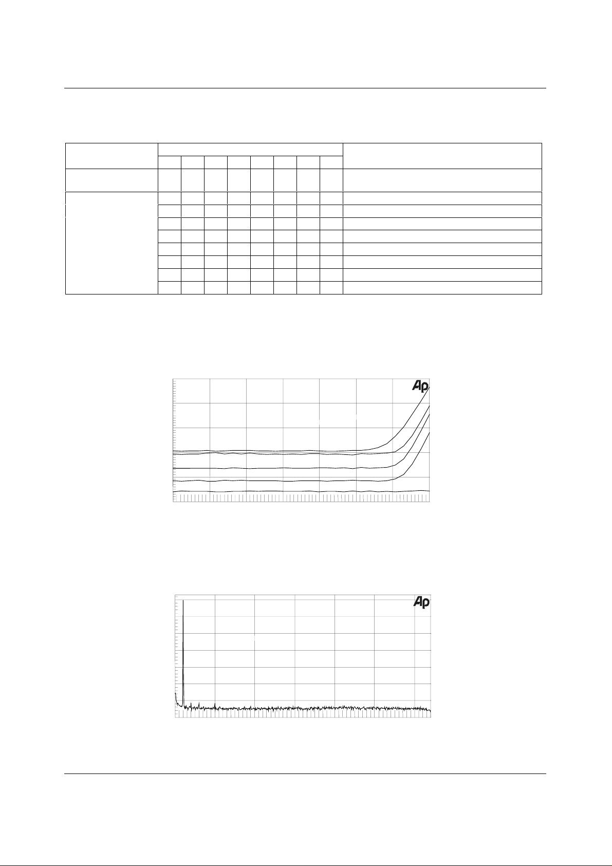
Figure 2 THD + Noise versus input level at gains of +6dB, 0dB, -6dB, -12dB and mute
+0
-20
-40
d
-60
B
V
-80
-100
-120
-140
5k 30k10k 15k 20k 25k
Frequency (Hz)
Figure 3 FFT of output signal with 1kHz, 1V rms sine w ave i nput
WOLFSON MICROELECTRONICS LTD AI Rev 1.1 September 2000
8
Page 9
Advanced Information WM8816
+0
-20
-40
d
-60
B
V
-80
-100
-120
-140
5k 30k10k 15k 20k 25k
Frequency (Hz)
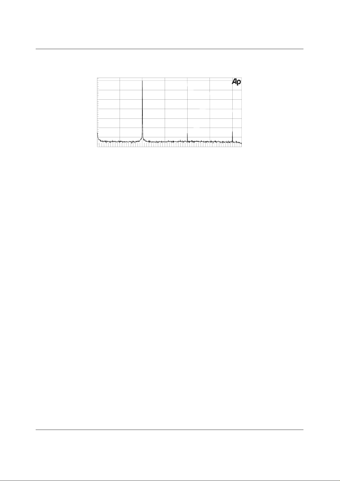
Figure 4 FFT of output signal with 10kHz, 1V rms sine w ave i nput
POWER SUPPLY DECOUPLING
For best audio performance, all digital activities should be avoided during analogue signal
processing. Special attenti on should be paid to power and ground decoupling. If possibl e separate
analogue and digital power supplies should be used. A cl ean analogue power supply should be us ed
for AVDD. DVDD should be the sam e as AV DD to avoid l atc h-up phenom ena. Dec oupling c apac itors
should be located as clos e t o the WM8816 as possible.
WOLFSON MICROELECTRONICS LTD AI Rev 1.1 September 2000
9
Page 10
WM8816 Advanced Information RECOMMENDED EXTERNAL COMPONENTS
LFO
LEFT CHANNEL
INPUT
RIGHT CHANNEL
INPUT
13
12
3
LIN
4
LMO
2
5
LGND
RFO
14
RIN
15
RMO
RGND
+18V
-
+
-18V
+18V
-
+
-18V
WM8816
Micro
Controller
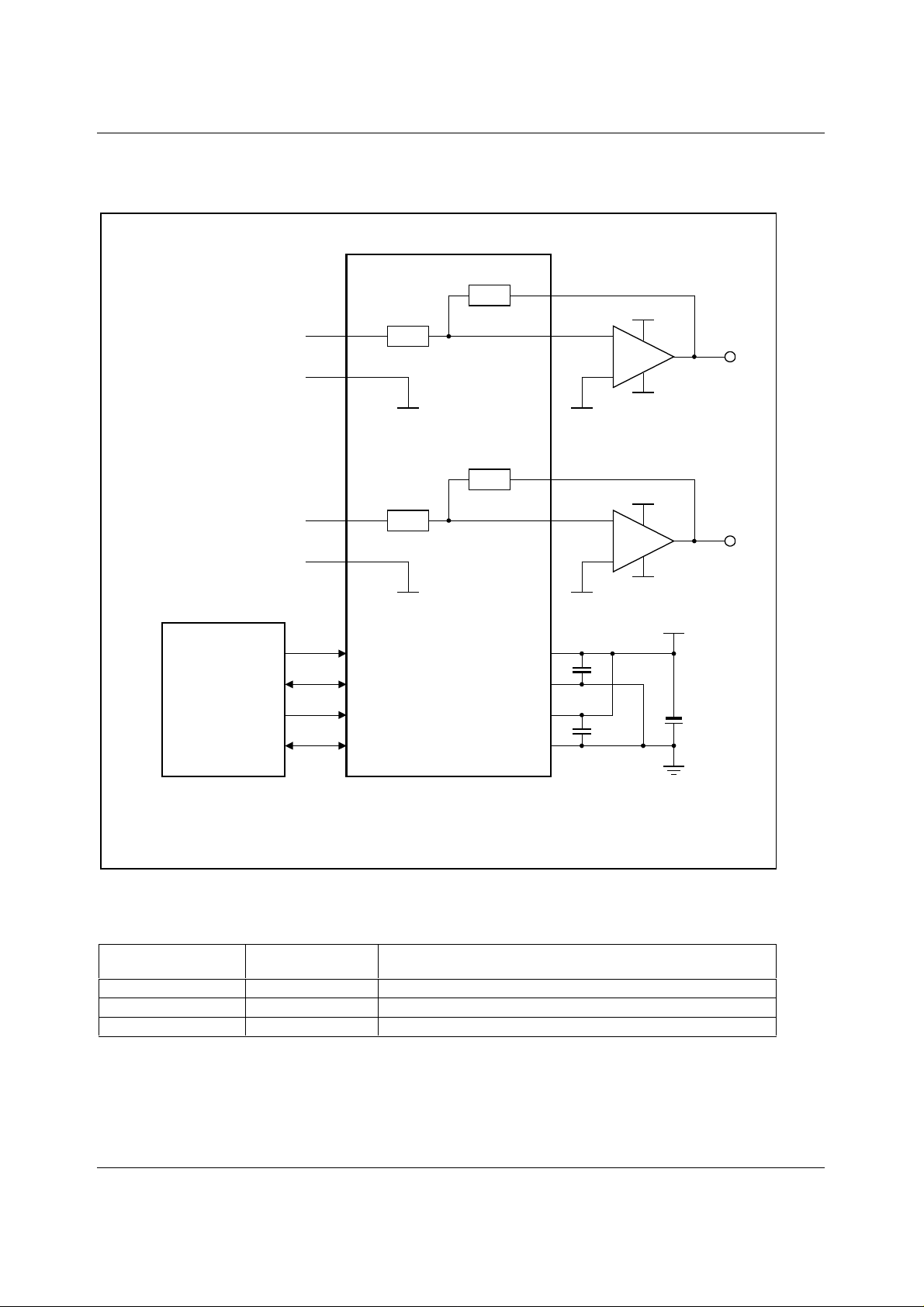
Note: Connect signal ground and non-inverting opamp input together on the PCB
Figure 5 Typical Application
10
6
9
8
CSB
DATA
CCLK
MUTEB
AVDD
AGND
DVDD
DGND
RECOMMENDED EXTERNAL COMPONENTS VALUES
COMPONENT
REFERENCE
C1 220nF Analogue Supply Decoupling
C2 220nF Digital Supply Decoupling
C3 10µF General Supply Decoupling
Table 3 Recommended External Components Values
SUGGESTED
VALUE
DESCRIPTION
1
16
7
11
C1
C2
+5V DC
+
C3
WOLFSON MICROELECTRONICS LTD AI Rev 1.1 September 2000
10
Page 11
Advanced Information WM8816
LFO
DAC
Balanced
Output
3
4
LIN
2
LMO
5
LGND
13
RIN
12
RGND
WM8816
RFO
RMO
14
15
+18V
-
+
+18V
-
+
-18V
-18V
2K 2K
+18V
-
+
2K
-18V
2K
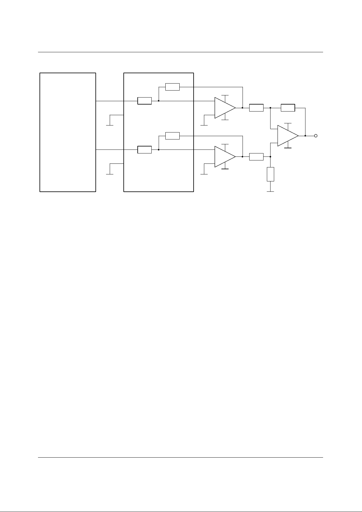
Figure 6 Configuration for Double Balanced Output (One Channel)
WOLFSON MICROELECTRONICS LTD AI Rev 1.1 September 2000
11
Page 12
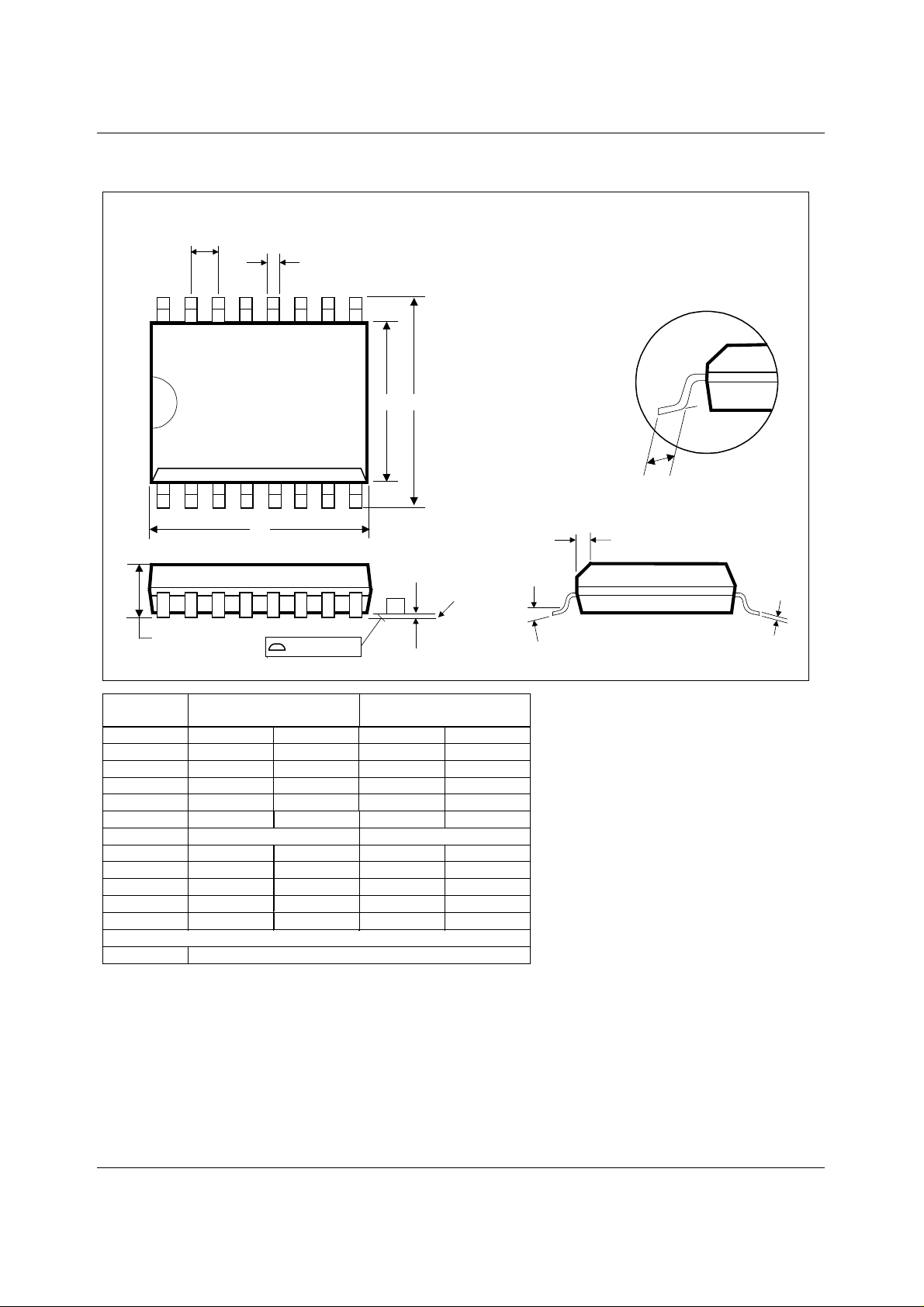
WM8816 Advanced Information PACKAGE DIMENSIONS
DW: 16 PIN SOICW 7.5mm (0.3") Wide Body, 1.27mm Lead Pitch
e
16
1
D
A
B
0.10 (0.004)
9
E H
8
A1
-C-
SEATING PLANE
DM019.A
L
o
h x 45
α
C
Symbols
Dimensions
(mm)
Dimensions
(Inches)
MINMAXMINMAX
A
A
1
B
2.35 2.65 0.0926 0.1043
0.10 0.30 0.0040 0.0118
0.33 0.51 0.0130 0.0200
C 0.23 0.32 0.0091 0.0125
D
10.10 10.50 0.3465 0.3622
e 1.27 BSC 0.0500 BSC
E
7.40 7.60 0.2914 0.2992
h 0.25 0.75 0.0100 0.0290
H
L 0.40 1.27 0.0160 0.0500
α
10.00 10.65 0.3940 0.4190
o
0
o
8
o
0
o
8
REF: JEDEC.95, MS-013
NOTES:
A. ALL LINEAR DIMENSIONS ARE IN MILLIMETERS (INCHES).
B. THIS DRAWING IS SUBJECT TO CHANGE WITHOUT NOTICE.
C. BODY DIMENSIONS DO NOT INCLUDE MOLD FLASH OR PROTRUSION, NOT TO EXCEED 0.25MM (0.010IN).
D. MEETS JEDEC.95 MS-013, VARIATION = AA. REFER TO THIS SPECIFICATION FOR FURTHER DETAILS.
WOLFSON MICROELECTRONICS LTD AI Rev 1.1 September 2000
12
 Loading...