

Page 1
WM8148
12-bit/12MSPS CCD/CIS Analogue Front End/Digitiser
Production Data, April 1999, Rev 4.0
DESCRIPTION
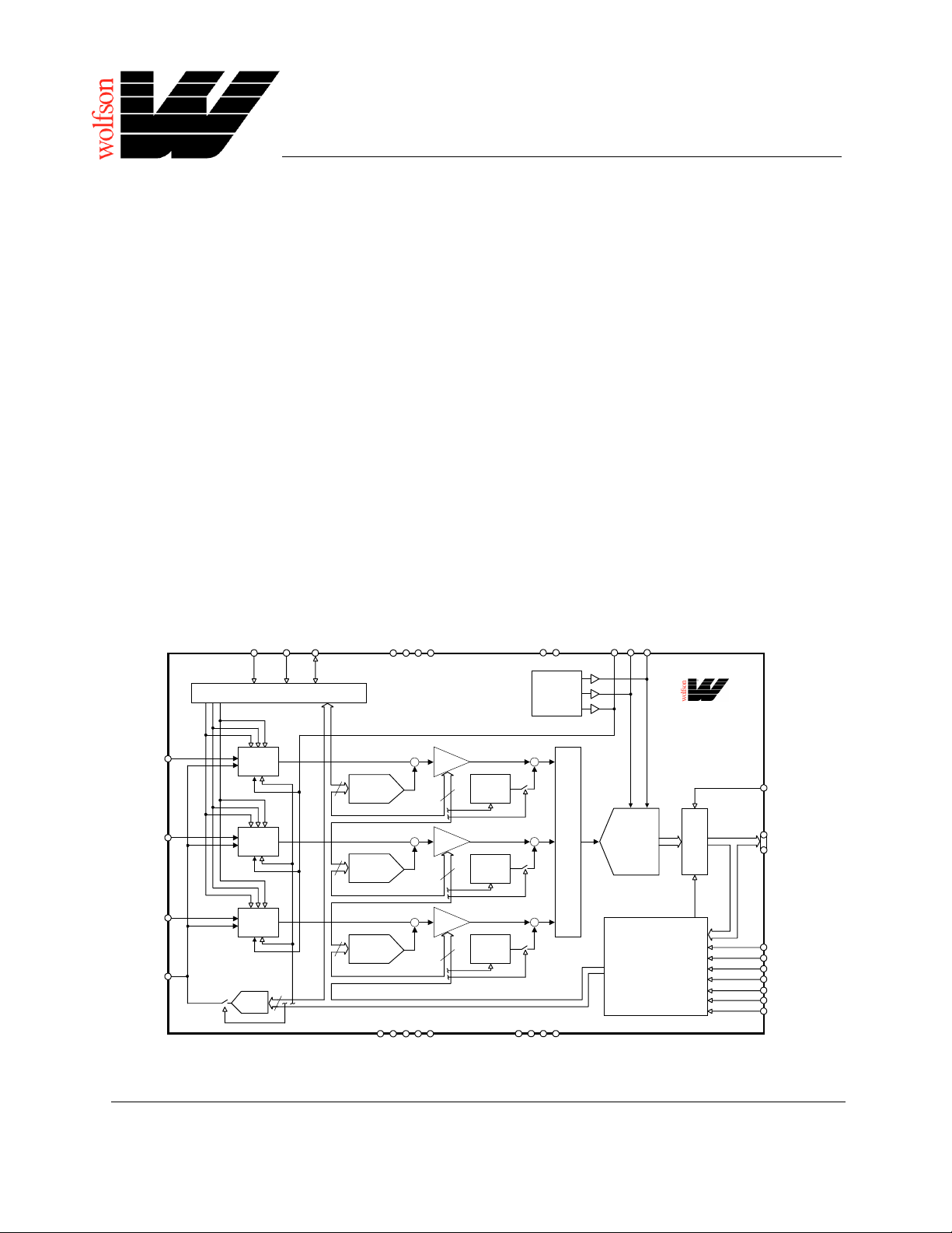
The WM8148 is a 12-bit, 12MSPS analogue front end/
digitiser IC, which interfaces to c olour or m onoc hrom e linear
array CCDs or contact image sensors (CIS). The device
includes all the signal conditioning circuitry required to
process the analogue signals from the CCD or CI S prior to
the internal ADC.
Three signal-processing channels are included in the
device. Each channel features reset level clamping,
correlated double sampling (CDS), offset correction and
programmable gain ampl ification (PGA). The output signal
from each channel is then multiplexed into a high
performance 12-bit analogue to digi tal converter (ADC).
The reset level clamp and/or CDS functions c an be selected
or bypassed depending on the application.
The WM8148 can be operated in several modes. The
operational mode of the device, including the sampling
scheme and power management is programmed via the
serial/parallel control i nt erface.
Output data is presented in either 12-bit parallel or bytewide (8+4-bit) format.
BLOCK DIAGRAM
VSMP
MCLK
RLC
(2)
(7)
(5)
AVDD 1- 4
(41,28,27,3)
FEATURES
•
Correlated double sampling
•
Programmable gain amplifier
•
Programmable input clamp voltage
•
Offset correction
•
12-bit, 12MSPS ADC
•
Internal voltage reference
•
12-bit or 8+4 bit data output mode
•
Single 5V supply or 5V analogue/3.3V digital supply
•
Programmable sample timing
•
Control interface compatible with previous Wolfson
AFEs
•
48-pin TQFP package
APPLICATIONS
•
Flatbed scanners
•
Document scanners
•
Multi-function peripherals (MFPs)
•
Colour copiers
•
Character recognition systems
•
Linear array CCDs
•
Contact image sensors (CIS)
VRB
VRT
DVDD1-2
(1,13)
VRX
(32)
(29)
(31)
RINP (36)
GINP (37)
BINP (39)
VRLC (33)
CL RS V
S
CDS
RLC
CDS
RLC
CDS
RLC
RLC
DAC
TIMING CONTROL
4
8
8
8
OFFSET
DAC
OFFSET
DAC
OFFSET
DAC
(35,40,30,25,6)
+
+ +
+
AGND1 - 5
WOLFSON MICROELECTRONICS LTD
Lutton Court, Bernard Terrace, Edi nburgh, EH8 9NX, UK
Tel: +44 (0) 131 667 9386
Fax: +44 (0) 131 667 5176
Email: [email protected]
http://www.wolfson.co.uk
PGA
PGA
PGA
6
6
6
± FULL
.
_
.
SCALE 2
± FULL
.
_
.
SCALE 2
± FULL
.
_
.
SCALE 2
VREF/BIAS
+
+
(8,24,4,26)
DGND1 - 4
MUX
WM8148
(43) OEB
12/8
12-BIT
ADC
CONFIGURABLE
SERIAL/PARALLEL
CONTROL INTERFACE
BIT
MUX
Production Data
OP[11:0]
(9-12,14-21)
(48) PNS
(34) OVRD
(45) SDI/DNA
(46) SCK/RNW
(47) SEN/STB
(42) NRESET
(44) SDO
contain final
specifications current on publication date.
Supply of products conf orms to Wol fson
Microelectronics' Terms and Conditions.
1999 Wolfson Microelectronics Ltd
.
Page 2
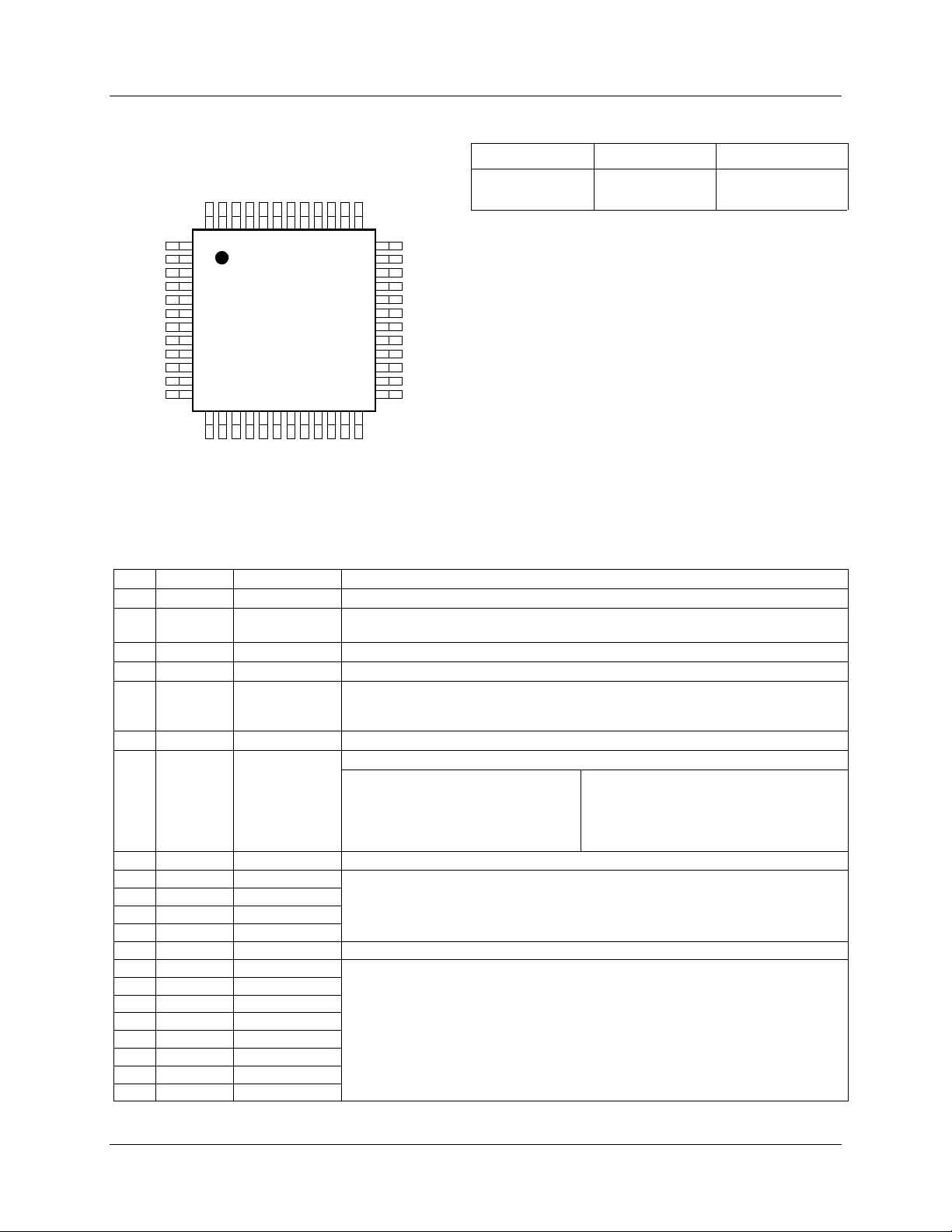
WM8148 PIN CONFIGURATION ORDERING INFORMATION
DEVICE TEMP. RANGE PACKAGE
Production Data
DVDD1
RLC
AVDD4
DGND3
MCLK
AGND5
VSMP
DGND1
OP0
OP1
OP2
OP3
PNS
1
2
3
4
5
6
7
8
9
10
11
12
13 14 15
DVDD2
SEN/STB
OP4
SDO
SDI/DNA
SCK/RNW
181920 21 22
OP5
OP6
OP7
OEB
NRESET
OP8NCOP9
AGND2
AVDD1
OP10
OP11
BINP
NC
3747 46 45 44 43 42 41 40 39 3848
242316 17
NC
GINP
36
35
34
33
32
31
30
29
28
27
26
25
DGND2
PIN DESCRIPTION
PIN NAME TYPE DESCRIPTION
1 DVDD1 Supply
2 RLC Digit al i nput
3 AVDD4 Supply
4 DGND3 Ground
5 MCLK Digital input
6 AGND5 Ground
7 VSMP Digital IO
8 DGND1 Ground
9 OP0 Digital output
10 OP1 Digital output
11 OP2 Digital output
12 OP3 Digital output
13 DVDD2 Supply
14 OP4 Digital IO
15 OP5 Digital IO
16 OP6 Digital IO
17 OP7 Digital IO
18 OP8 Digital IO
19 OP9 Digital IO
20 OP10 Digital IO
21 OP11 Digital IO
Digital supply (3.3V to 5V ) f or di gi tal inputs and SDO.
Selects whether reset level c l amp is applied, active high. If RLC is required on every
pixel then this pin can be tied high.
Analogue supply (5V).
Digital ground (0V).
Master clock. This clock is applied at N times the input pixel rate (N = 12, 8, 6, or
4 dependent on input sampling mode). MCLK is divided internally by N to generate
internal clocks and to provide the clock source for digital logic.
Analogue ground (0V).
Video sample synchronisation pulse. This pin m ay be ei t her an i nput (default) or output.
Input: This signal is pul sed externally
to synchronise the WM8148’s video
input sample instant and the N-phase
internal clock to CCD clocks and
interface bus tim i ng.
Digital ground (0V) for output drivers.
12-bit signal data output bus. Data is output MSB on OP[11] and LSB on pin OP[0].
See description of pins 14-21 for mode definitions.
Digital supply (3.3V-5V) for Di gi tal IO pins and OP0 to OP3
12-bit bi-directional data bus. On pins OP[4] to OP[11], signal data is output if OE B = 0
and register write data is input if OE B = 1.
There are five main modes:
• Hi-Z: when OEB = 1
• Output 12-bit: twelve bit signal dat a output from bus
• Output 8-bit muxed: signal dat a out put on OP[11:4] at 2 ∗ ADC conversion rate
• Input 8-bit: register write data i nput on OP[11:4]
• Output 8-bit: register readbac k data output on OP[11:4]
RINP
AGND1
OVRD
VRLC
VRX
VRT
AGND3
VRB
AVDD2
AVDD3
DGND4
AGND4
XWM8148CFT/V 0 to 70oC
Output: This signal is pul sed internally to
flag the video input sampl e i nstant, to allow
the CCD clocks and interface bus to be
synchronised to the WM8148.
48-pin 1mm
thick body TQFP
WOLFSON MICROELECTRONICS LTD
PD Rev 4.0 April 1999
2
Page 3
WM8148
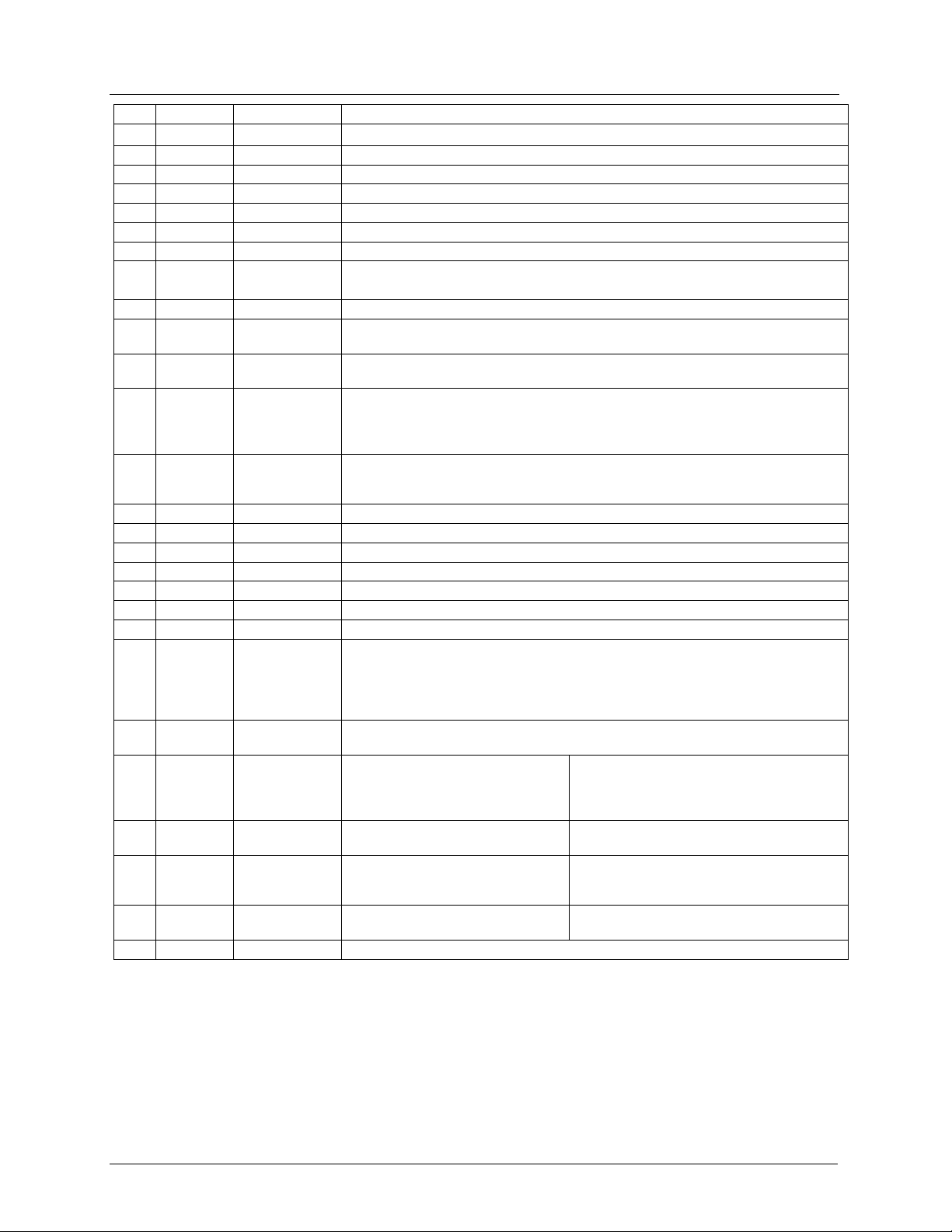
PIN NAME TYPE DESCRIPTION
22 NC
23 NC
24 DGND2 Ground
25 AGND4 Ground
26 DGND4 Ground
27 AVDD3 Supply
28 AVDD2 Supply
29 VRB Analogue output
30 AGND3 Ground
31 VRT Analogue output
32 V RX Analogue output
33 V RLC Analogue IO
34 OVRD Analogue input
35 AGND1 Ground
36 RI NP Analogue input
37 GINP Analogue input
38 NC
39 BINP Anal ogue i nput
40 AGND2 Ground
41 AVDD1 Supply
42 NRESET Digital input
43 OEB Digital i nput
44 SDO Digital output
45 SDI/DNA Digital input
46 SCK/RNW Digital i nput
47 SEN/STB Digital input
48 PNS Digital input
No internal connection.
No internal connection.
Digital ground (0V) for output drivers.
Analogue ground (0V).
Digital ground (0V).
Analogue supply (5V).
Analogue supply (5V).
Lower reference voltage. This pin mus t be connected to AGND and VRT via decoupli ng
capacitors. See Recommended External Components section for details.
Analogue ground (0V).
Upper reference voltage. This pin must be connected to AGND and VRB via decoupling
capacitors. See Recommended External Components section for details.
Input return bias voltage. This pin must be connected t o AGND via decoupling
capacitors. See Recommended External Components section for details.
Selectable analogue output volt age f or RLC or single-ended bias reference.
This pin would typically be connected t o A G ND vi a a decoupling capacitor.
See Recommended External Components section for detai l s. VRLC can be externally
driven if programmed Hi-Z.
Override pin. Typically tied low externally.
The sense of this pin defines the device function on reset . Refer to the description of
pin 42 for details.
Analogue ground (0V).
Red channel input video.
Green channel input video.
No internal connection.
Blue channel input video.
Analogue ground (0V).
Analogue supply (5V).
Reset input, active low. This signal forces a reset of al l i nt ernal regi sters.
Registers are set to defaul ts if pin OVRD is tied low.
If pin OVRD is tied high t hen al l regi sters are set to defaults except EN which is set to
1 and RLCEXT which is set to 0. This will turn on all analogue circuitry including the RLC
DAC buffers driving the VRLC pi n.
Output enable control, all out puts disabled when OEB = 1.
This pin must be externally connec ted.
Serial Interface: register read-back,
VSMP output, setup error fl ag or
over-range flag (depending on control
bits SDO [1:0]).
Serial interface:
serial input data signal.
Serial interface: seri al clock signal. Parallel interface:
Serial interface: enable pulse,
active high.
Low = serial interface, High = parallel i nt erface. This pin must be externall y c onnected.
Production Data
Parallel Interface: Hi-Z, VSMP output, set-up
error flag or over-range flag (depending on
control bits SDO [1:0]).
Parallel interface: High = data, Low = address.
High = OP[11:4] is output bus,
Low = OP[11:4] is input bus (Hi-Z).
Parallel interface: s trobe, active low.
WOLFSON MICROELECTRONICS LTD
PD Rev 4.0 April 1999
3
Page 4
WM8148
Production Data
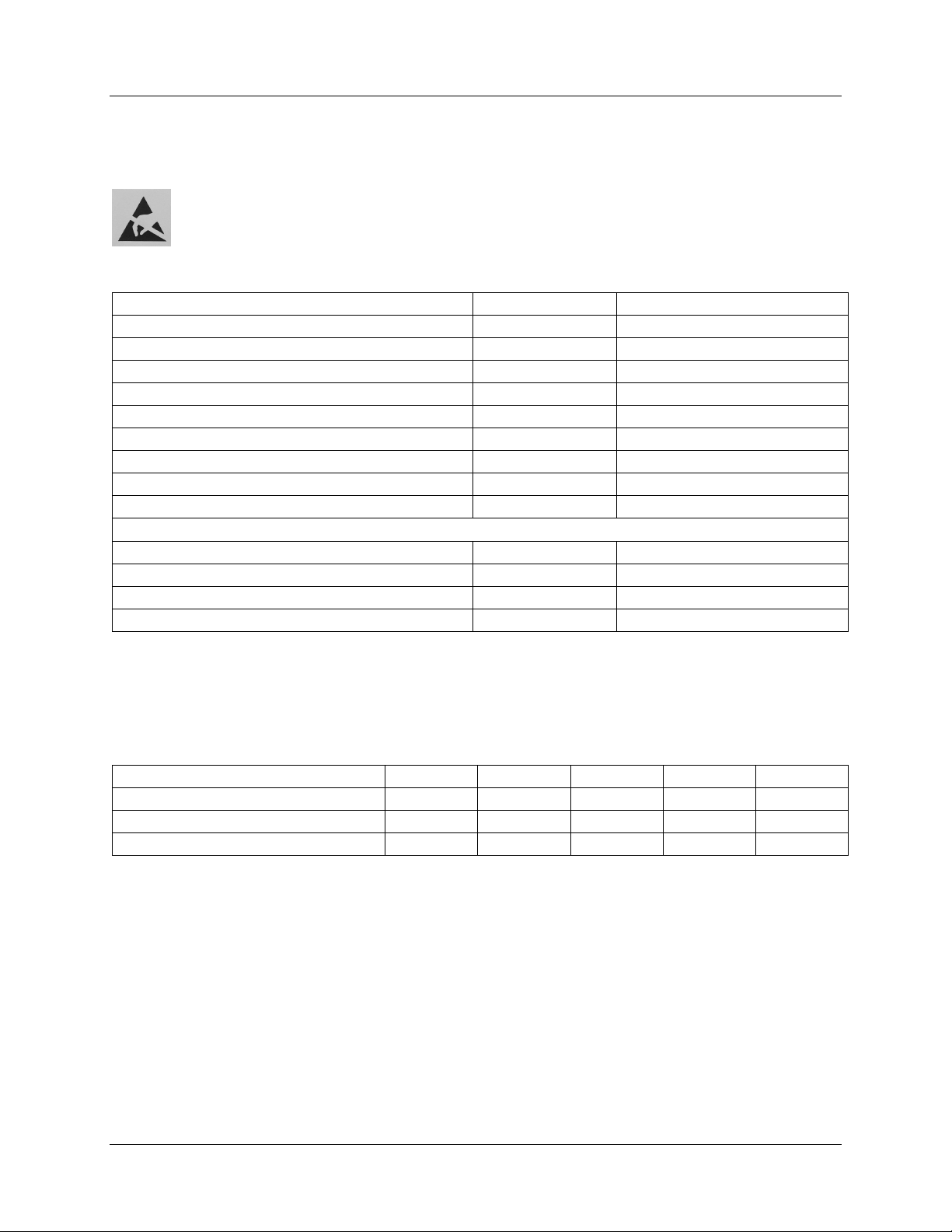
ABSOLUTE MAXIMUM RATINGS
Absolute Maximum Ratings are stress rat ings only. Perm anent dam age to the device m ay be caused by continuous ly operating at
or beyond these limits. Device functional operating limits and guarant eed performance specifications are given under E lectrical
Characteristics at the test conditions s pec i fied
ESD Sensitive Device. This device is manufact ured on a CMOS process. It is t herefore generically susceptible
to damage from excessive static voltages. Proper ESD precautions must be taken during handling and storage
of this device.
As per JEDEC specif i cations A112-A and A113-B, thi s product requires specific storage conditions prior to surface mount assembly
and will be supplied in vacuum-sealed moisture barrier bags. I t has been classified as having a Moisture Sensitivity Level of 2.
CONDITION MIN MAX
Analogue supply voltages: A VDD1 − 4
Digital supply voltages: DVDD1 − 2
Digital grounds: DGND1 − 4
Analogue grounds: AGND1 − 5
Digital inputs and SDO
Digital outputs (not SDO)
Digital IO pins
RINP, GINP, BI NP
Other pins
GND - 0.3V GND + 7V
GND - 0.3V GND + 7V
GND - 0.3V GND + 0.3V
GND - 0.3V GND + 0.3V
GND - 0.3V DVDD1 + 0.3V
GND - 0.3V DVDD2 + 0.3V
GND - 0.3V DVDD2 + 0.3V
GND - 0.3V AVDD + 0.3V
GND - 0.3V AVDD + 0.3V
Operating temperature range: T
Storage temperature
Lead temperature (soldering, 10 s econds)
Lead temperature (soldering, 2 minutes)
Notes:
• GND denotes the voltage of any ground pin. AVDD denotes the voltage applied to any AV DD pi n.
• AGND and DGND pins are intended to be operated at the same potential. Differential voltages between these pins will degrade
performance.
A
0°C+70°C
-50°C +150°C
+260°C
+183°C
RECOMMENDED OPERATING CONDITIONS
CONDITION SYMBOL MIN TYP MAX UNITS
Operating temperature range
Digital input and output s uppl y vol tages
Analogue supply voltages
T
A
DVDD1 − 2 2.97 5 5.25 V
AVDD1 − 4 4.75 5 5.25 V
070°C
WOLFSON MICROELECTRONICS LTD
PD Rev 4.0 April 1999
4
Page 5
WM8148
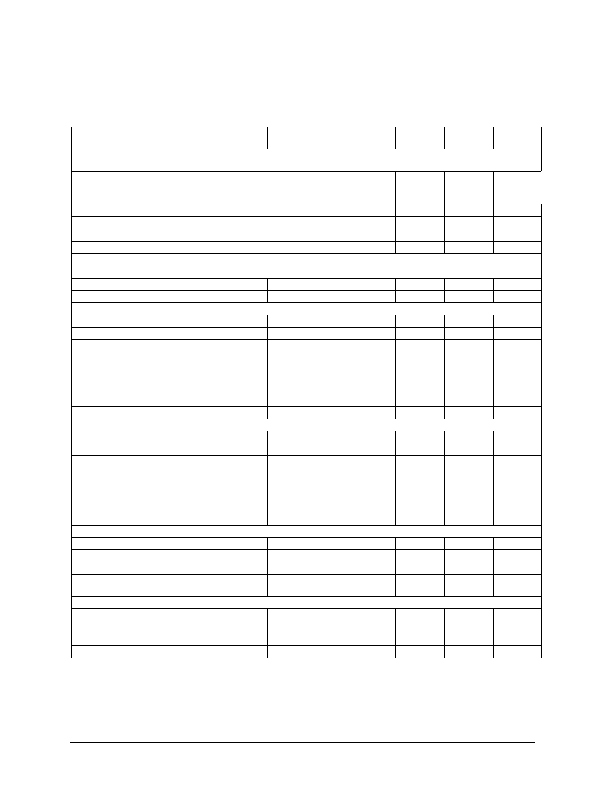
ELECTRICAL CHARACTERISTICS
TEST CONDITIONS
AVDD = 4.75 to 5.25V, DVDD1 and DV DD2 = 2.97 to 5.25V, AGND = DGND = 0V, T
otherwise stated (AVDD denotes the voltage applied to all AVDD pins).
PARAMETER SYMBOL TEST
CONDITIONS
Overall System Performance Including 12-bit ADC, PGA, Offset and CDS Functions
NO MISSING CODES GUARANTEED
Full-scale input voltage range
Max Gain 0.413 V
Gain = 1.0 3.0 V
Min Gain 4.13 V
Zero-scale transition error
Full-scale transition error
Differential non-linearit y
Integral non-linearity
DNL Gain = 1.0 0.25 1.00 LSB
INL Gain = 1.0 1.0 LSB
Gain = 1.0 20 mV
Gain = 1.0 20 mV
ANALOGUE SPECIFICATION
Input Multiplexer
Channel to channel gain matchi ng
Input voltage range
V
IN
References
Upper reference voltage
Lower reference voltage
Input return bias voltage
Diff. reference voltage (VRT-VRB)
Output resistance VRT, V RB , V RX
VRT 3.00 3.30 3.60 V
VRB 1.50 1.80 2.10 V
VRX 1.50 1.75 2.00 V
V
RTB
VRT, VRB, VRX
buffers enabled
Resistance VRT to VRB
VRT, VRB buffers
disabled
VRX Hi-Z leakage current
VRX buffer disabled 1 µA
VRLC/Reset-Level Clamp (RLC)
RLC switching impedance
VRLC Hi-Z leakage current
VRLC = 0 to AVDD 1 µA
VRLC DAC resolution
VRLC DAC step
AVDD = 5V 290 333 370 mV/step
VRLC short-circuit current
VRLC output resistance
VRLC = AVDD
VRLC = 0V
VRLC = other
Offset DAC
Resolution
Differential non-linearit y
Integral non-linearity
Output voltage
DNL -0.25 0.05 0.25 LSB
INL -0.50 0.10 0.50 LS B
Code 00(hex)
Code FF(hex)
Programmable Gain Amplifier. Monotonicity Guaranteed
Resolution
Max gain, each channel
Min gain, each channel
G
MAX
G
MIN
Gain error, each channel
MIN TYP MAX UNIT
0 AVDD V
1.30 1.50 1.70 V
500 800 1100 Ω
4bits
8bits
6bits
Production Data
= 0 to 70°C, MCLK = 48MHz unless
A
1%
2 Ω
75 Ω
5mA
80
80
5
-200
200
7.4 V/V
0.74 V/V
25%
Ω
Ω
Ω
mV
mV
WOLFSON MICROELECTRONICS LTD
PD Rev 4.0 April 1999
5
Page 6
WM8148
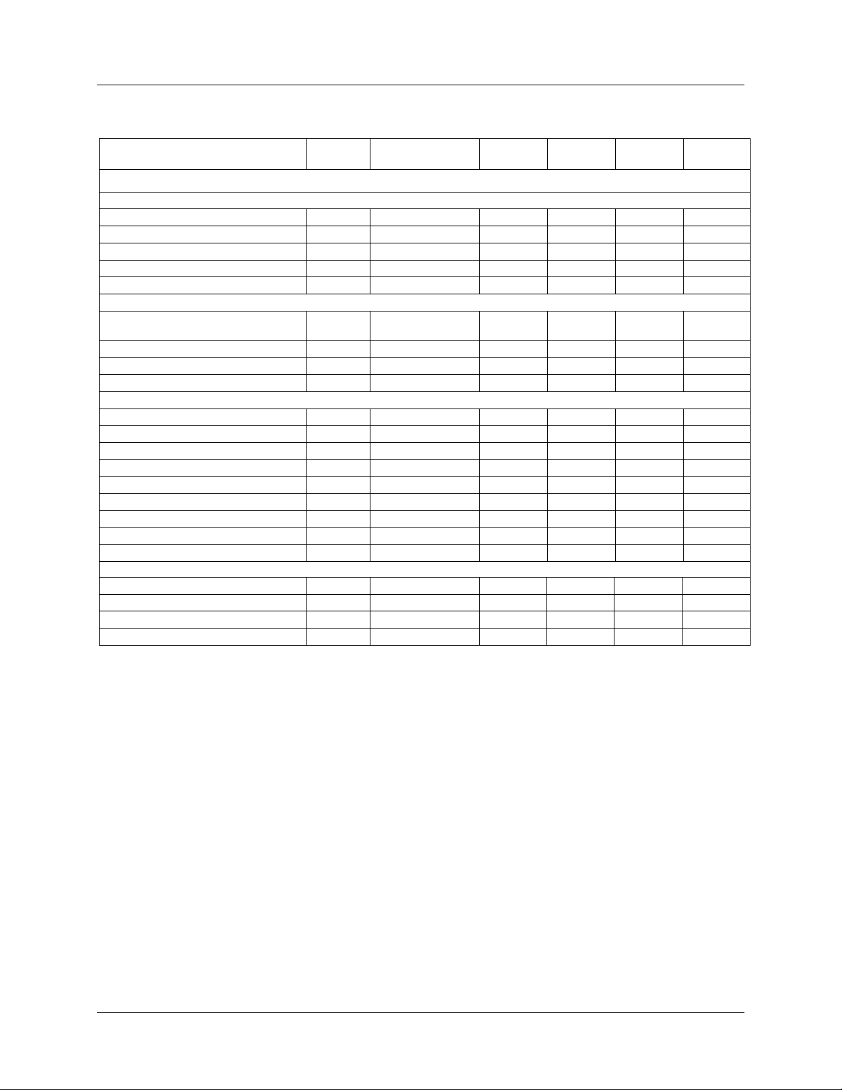
TEST CONDITIONS
AVDD = 4.75 to 5.25V, DVDD1 and DV DD2 = 2.97 to 5.25V, AGND = DGND = 0V, T
otherwise stated (AVDD denotes the voltage applied to all AVDD pins).
PARAMETER SYMBOL TEST
DIGITAL SPECIFICATIONS
Digital Inputs
High level input voltage
Low level input voltage
High level input current
Low level input current
Input capacitance
V
IH
V
IL
I
IH
I
IL
C
I
Digital Outputs
High level output voltage
Low level output voltage
High impedance output current
V
OH
V
OL
I
OZ
Output rise/fall time
Digital IO Pins
Applied high level input voltage
Applied low level input voltage
High level output voltage
Low level output voltage
Low level input current
High level input current
High impedance output current
V
IH
V
IL
V
OH
V
OL
I
IL
I
IH
I
OZ
Output rise/fall time
Input capacitance
C
I
SUPPLY CURRENTS
Total supply current – act i ve
Total analogue supply current – acti ve I
Total digital supply c urrent – active I
AVDD
DVDD
Supply current – disabled
CONDITIONS
0.8 ∗ DVDD1 V
IOH = 1mA, DVDD =
DVDD - 0.5 V
DVDD1 or DVDD2
IOL = 1mA 0.5 V
C
= 10pF 3 ns
LOAD
0.8 ∗ DVDD2 V
IOH = 1mA DVDD2 - 0.5 V
IOL = 1mA 0.5 V
C
= 10pF 3 ns
LOAD
Production Data
= 0 to 70°C, MCLK = 48MHz unless
A
MIN TYP MAX UNIT
0.2 ∗ DVDD1 V
1 µA
1 µA
5pF
1 µA
0.2 ∗ DVDD2 V
1 µA
1 µA
1 µA
5pF
75 100 mA
73 mA
2mA
110µA
WOLFSON MICROELECTRONICS LTD
PD Rev 4.0 April 1999
6
Page 7
WM8148
Production Data
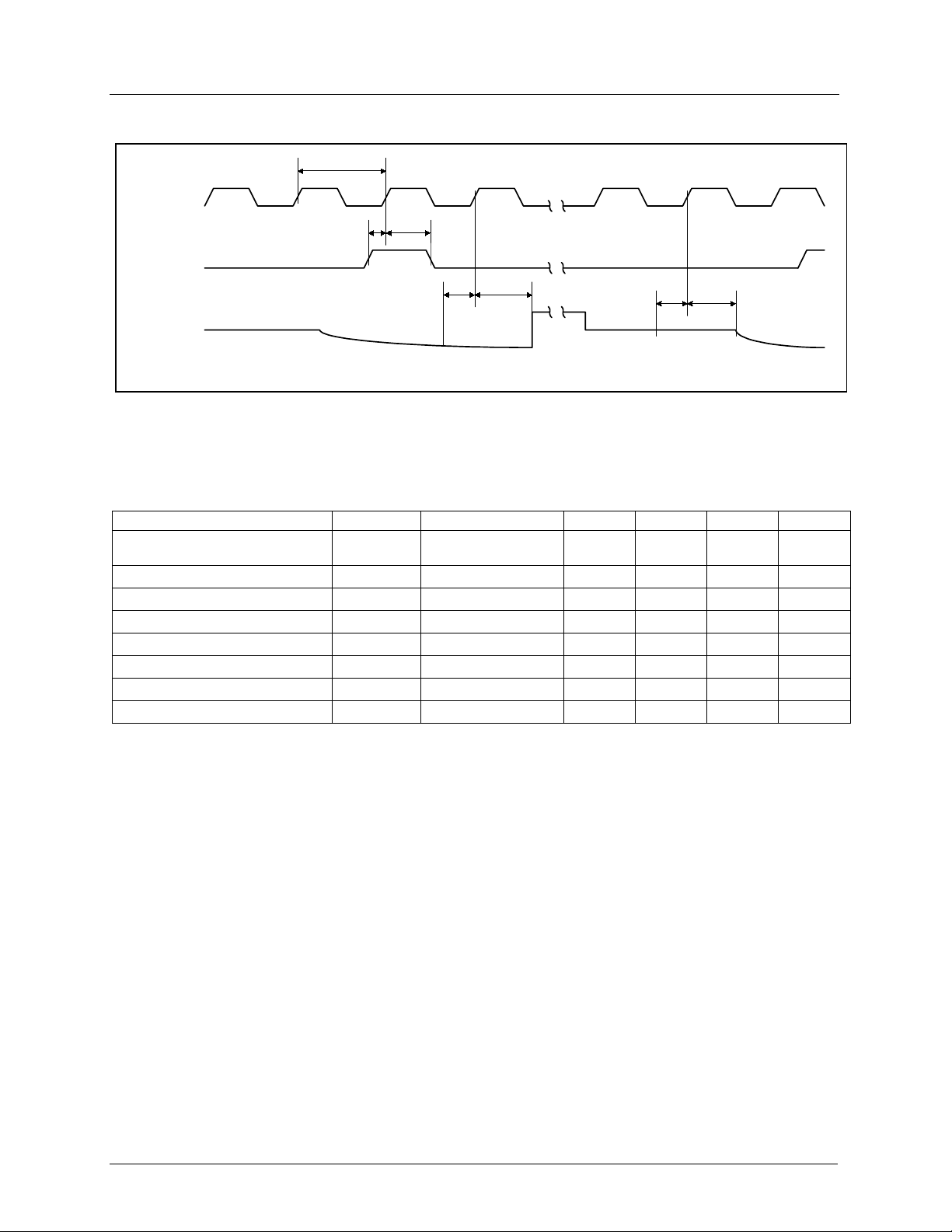
INPUT VIDEO SAMPLING (EXTERNAL VSMP)
t
PER
MCLK
t
PER
t
VSMPSU
t
VSMPH
t
VSU
t
VH
t
RSU
t
RH
t
VSMPH
t
VSUtVH
t
RSUtRH
= 0 to 70°C, MCLK = 48MHz unless
A
20.8 ns
45 55 %
2ns
5ns
10 ns
10 ns
10 ns
10 ns
t
VSMPSU
VSMP
INPUT
VIDEO
Figure 1 Input Video Timing (External VSMP)
TEST CONDITIONS
AVDD = 4.75 to 5.25V, DVDD1 and DVDD2 = 2.97 to 5.25V, AGND = DGND = 0V, T
otherwise stated (AVDD denotes the voltage applied to all AVDD pins).
PARAMETER SYMBOL TEST CONDITIONS MIN TYP MAX UNITS
MCLK period
(dependent on mode selected)
MCLK duty cycle
VSMP set-up time
VSMP hold time
Video level set-up tim e
Video level hold time
Reset level set-up time
Reset level hold tim e
Notes:
1. t
VSU
and t
denote the set-up time requi red f rom when the input video signal has settled.
RSU
2. The reset sample point may be relative to either the risi ng or the falling edge of MCLK, depending on the setting of
control bits RESREF[3:0].
3. Parameters are meas ured at 50% of the rising/falli ng edge.
WOLFSON MICROELECTRONICS LTD
PD Rev 4.0 April 1999
7
Page 8
WM8148
Production Data
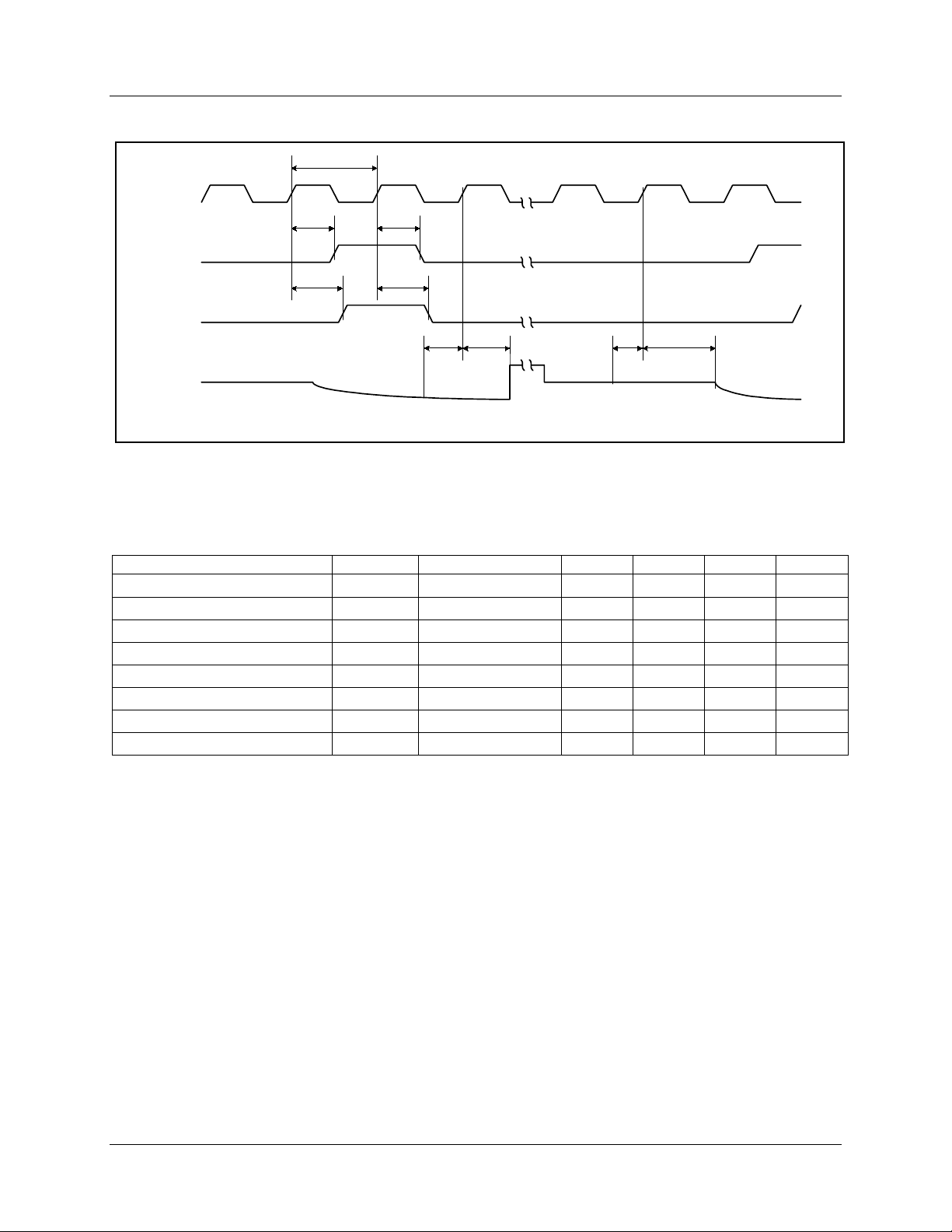
INPUT VIDEO SAMPLING (INTERNAL VSMP)
t
PER
MCLK
t
VSMPPD
VSMP,
OUTPUT
t
SDOPD
SDO,
OUTPUT
VIDEO
Figure 2 Input Video Timing (Internal VSMP)
TEST CONDITIONS
AVDD = 4.75 to 5.25V, DVDD1 and DV DD2 = 2.97 to 5.25V, AGND = DGND = 0V, T
otherwise stated (AVDD denotes the voltage applied to all AVDD pins).
PARAMETER SYMBOL TEST CONDITIONS MIN TYP MAX UNITS
MCLK period
MCLK duty cycle
VSMP output propagation delay
SDO output propagation delay
Video level set-up tim e
Video level hold time
Reset level set-up time
Reset level hold tim e
1. t
Notes:
VSU
and t
denote the set-up time requi red f rom when the input video signal has settled.
RSU
2. The reset sample point may be relative to either the risi ng or the falling edge of MCLK, depending on the setting of
control bits RESREF[3:0].
3. Parameters are meas ured at 50% of the rising/falli ng edge.
t
PER
t
VSMPPD
t
SDOPD
t
VSU
t
VH
t
RSU
t
RH
t
VSMPPD
t
SDOPD
t
VSUtVH
C
LOAD
C
LOAD
t
RSU
= 0 to 70°C, MCLK = 48MHz unless
A
t
RH
20.8 ns
45 55 %
= 10pF 15 25 ns
= 10pF 20 35 ns
10 ns
10 ns
10 ns
10 ns
WOLFSON MICROELECTRONICS LTD
PD Rev 4.0 April 1999
8
Page 9
WM8148
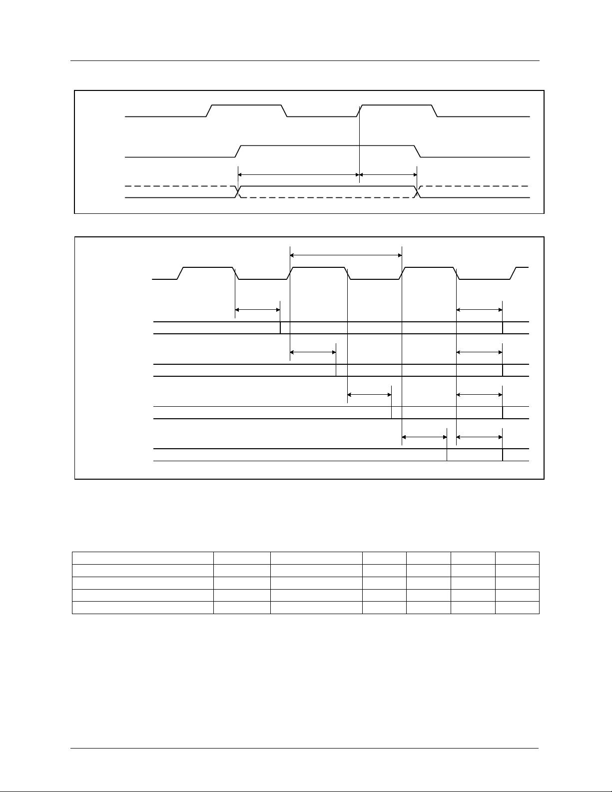
RESET LEVEL CLAMP
MCLK
VSMP
RLC = 0
RLC = 1
Figure 3 Reset Level Clamp Control Timing
MCLK
t
RLCSU
t
PER
t
RLCH
Production Data
CL
CL
CL
CL
MODE 8-13
SMALL = 0
MODE 8-13
SMALL = 1
MODE 0-5
SMALL = 0
MODE 0-5
SMALL = 1
t
RLCPD
OFF ON OFF
t
RLCPD
OFF ON OFF
t
RLCPD
OFF O N OFF
t
RLCPD
OFF O N OFF
t
RLCPD
t
RLCPD
t
RLCPD
t
RLCPD
Figure 4 Internal Clamp Signal (CL) Timing
TEST CONDITIONS
AVDD = 4.75 to 5.25V, DVDD1 and DV DD2 = 2.97 to 5.25V, AGND = DGND = 0V, T
= 0 to 70°C, MCLK = 48MHz unless
A
otherwise stated (AVDD denotes the voltage applied to all AVDD pins).
PARAMETER SYMBOL TEST CONDITIONS M IN TYP M AX UNITS
MCLK period
Propagation delay t
Set-up time t
Hold time t
1. Internal clamp signal (CL) timing may be relative to either the falling or ris i ng edge of MCLK depending on t he setting of
Notes:
t
PER
RLCPD
RLCSU
RLCH
20.8 ns
15 ns
10 ns
10 ns
control bits RESREF[3:0].
2. Parameters are meas ured at 50% of the rising/falli ng edge.
WOLFSON MICROELECTRONICS LTD
PD Rev 4.0 April 1999
9
Page 10
WM8148
OUTPUT DATA
OEB
Production Data
t
PZE
OP[11:0]
Hi-Z
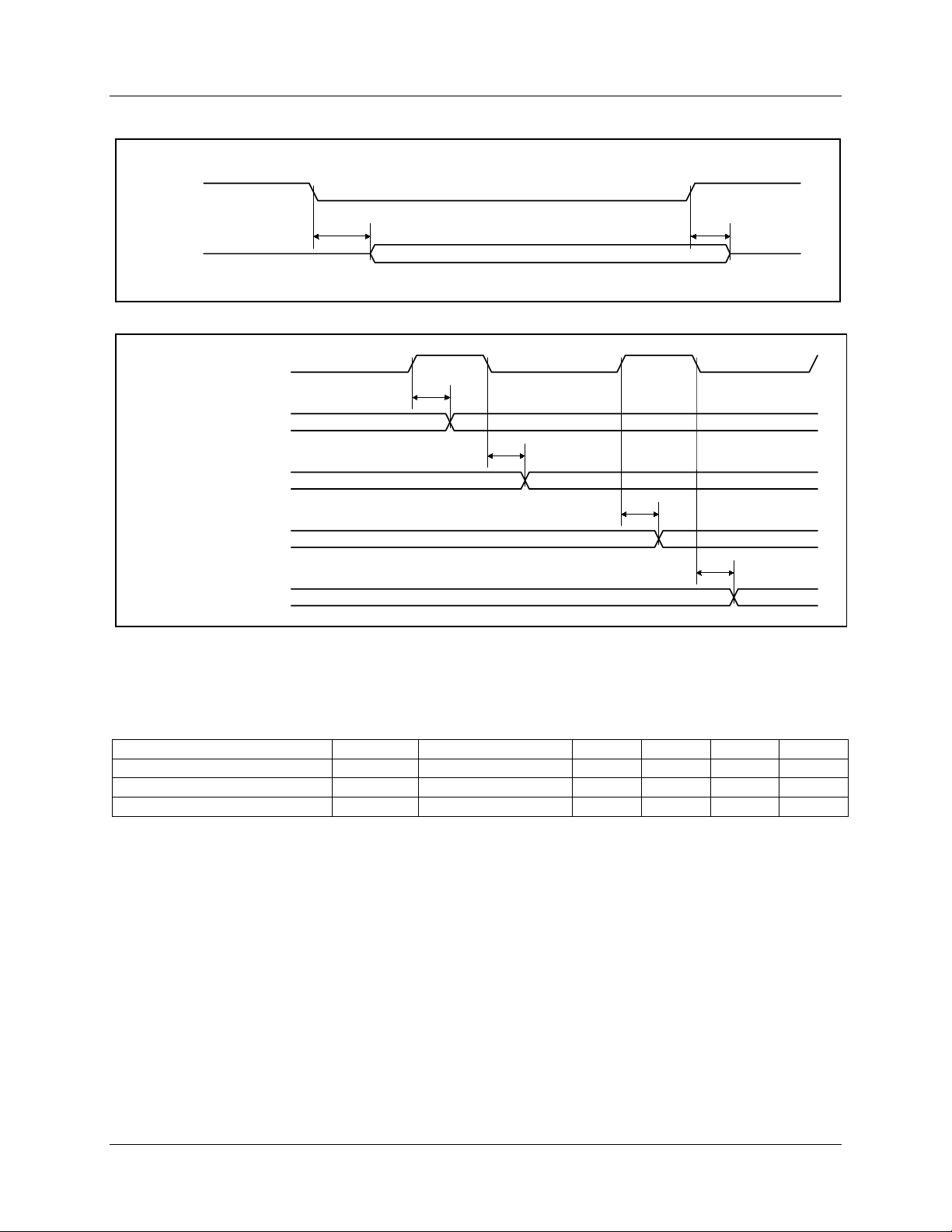
Figure 5 Output Data Enable Timing
MCLK
t
PD
FDEL[1:0] = 01
FDEL[1:0] = 00
OP[11:0]
OP[11:0]
t
PD
DEFAULT
FDEL[1:0] = 10
FDEL[1:0] = 11
OP[11:0]
OP[11:0]
Figure 6 Output Data Timing (Including Fine Latency Control By FDEL[1:0])
t
PEZ
Hi-Z
t
PD
t
PD
TEST CONDITIONS
AVDD = 4.75 to 5.25V, DVDD1 and DV DD2 = 2.97 to 5.25V, AGND = DGND = 0V , T
= 0 to 70°C, MCLK = 48MHz unless
A
otherwise stated (AVDD denotes the voltage applied to all AVDD pins).
PARAMETER SYMBOL TEST CONDITIONS MIN TYP MAX UNITS
Output propagation delay t
Output enable time t
Output disable time t
Parameters are meas ured at 50% of the rising/falli ng edge.
Note:
PD
PZE
PEZ
IOH = 1mA, IOL = 1mA102030ns
15 ns
15 ns
WOLFSON MICROELECTRONICS LTD
PD Rev 4.0 April 1999
10
Page 11
WM8148
SERIAL INTERFACE
Production Data
t
SPER
t
SCKLtSCKH
SCK
t
SSU
t
SH
SDI
t
SCE
t
SEWtSEC
SEN
t
SESD
t
SCSD
t
SCSDZ
SDO
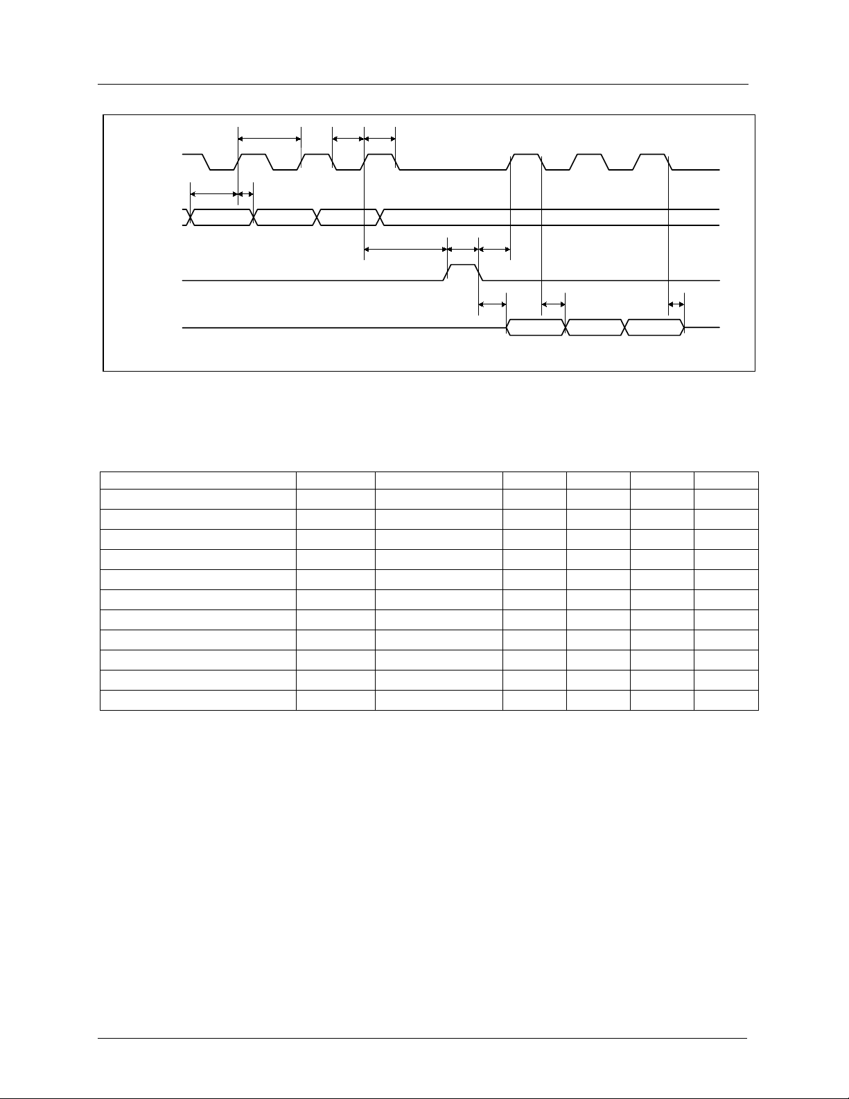
Figure 7 Serial Interface Timing
TEST CONDITIONS
AVDD = 4.75 to 5.25V, DVDD1 and DV DD2 = 2.97 to 5.25V, AGND = DGND = 0V , T
= 0 to 70°C, MCLK = 48MHz unless
A
otherwise stated (AVDD denotes the voltage applied to all AVDD pins).
PARAMETER SYMBOL TEST CONDITIONS MIN TYP MAX UNITS
SCK period
SCK high
SCK low
SDI set-up time
SDI hold time
SCK to SEN set-up time
SEN to SCK set-up time
SEN pulse width
SEN low to SDO out
SCK low to SDO out
SCK low to SDO high impedance
Parameters are meas ured at 50% of the rising/falli ng edge.
Note:
t
SPER
t
SCKH
t
SCKL
t
SSU
t
SH
t
SCE
t
SEC
t
SEW
t
SESD
t
SCSD
t
SCSDZ
83.3 ns
20 ns
20 ns
10 ns
10 ns
20 ns
20 ns
50 ns
35 ns
35 ns
25 ns
WOLFSON MICROELECTRONICS LTD
PD Rev 4.0 April 1999
11
Page 12
WM8148
PARALLEL INTERFACE
STB
t
STB
Production Data
D[11:4]
ADC DATA OUT
t
ASU
Z
t
ADLStADLHtADHStADHH
t
AHtDSU
t
DH
DATA INADDRESS IN
Z
ADC DATA OUT DATA OUT
t
STDO
t
STAO
ADC DATA OUT
DNA
t
OPZ
t
OPD
RNW
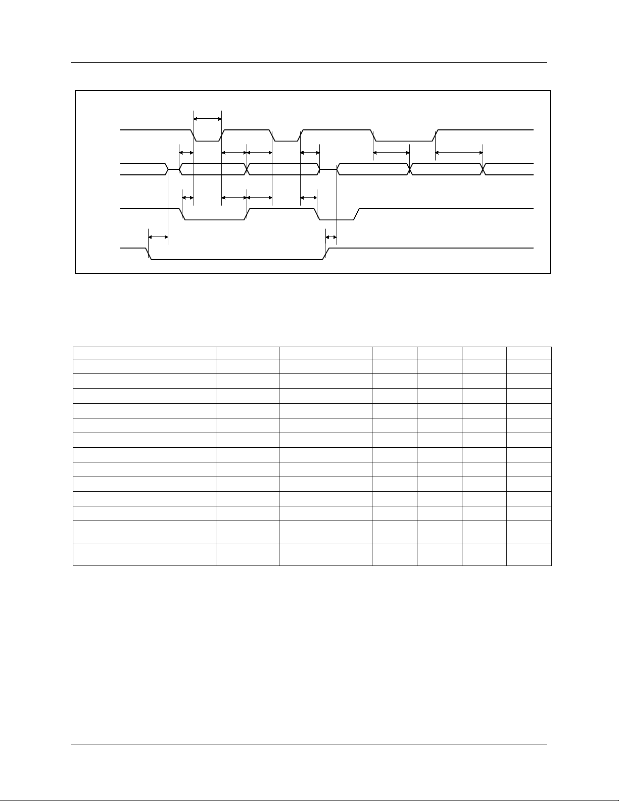
Figure 8 Parallel Interface Timing
TEST CONDITIONS
AVDD = 4.75 to 5.25V, DVDD1 and DV DD2 = 2.97 to 5.25V, AGND = DGND = 0V , T
= 0 to 70°C, MCLK = 48MHz unless
A
otherwise stated (AVDD denotes the voltage applied to all AVDD pins).
PARAMETER SYMBOL TEST CONDITIONS MIN TYP M AX UNITS
RNW Low to OP[11:4] Hi -Z.
Address set-up time to STB Low
DNA Low set-up time to STB Low
Strobe Low time
Address hold time f rom STB High
DNA Low hold time from S T B High
Data set-up time to STB Low
DNA High set-up time to STB Low
Data hold time from STB High
Data High hold time from STB High
RNW High to OP[11:4] output
Data output propagation delay from
t
t
t
ADLS
t
t
t
ADLH
t
t
ADHS
t
t
ADHH
t
t
STDO
OPZ
ASU
STB
AH
DSU
DH
OPD
20 ns
10 ns
10 ns
50 ns
10 ns
10 ns
10 ns
10 ns
10 ns
10 ns
35 ns
35 ns
STB Low
ADC data out propagation delay
t
STAO
35 ns
from STB High
Parameters are meas ured at 50% of the rising/falli ng edge.
Note:
WOLFSON MICROELECTRONICS LTD
PD Rev 4.0 April 1999
12
Page 13
WM8148
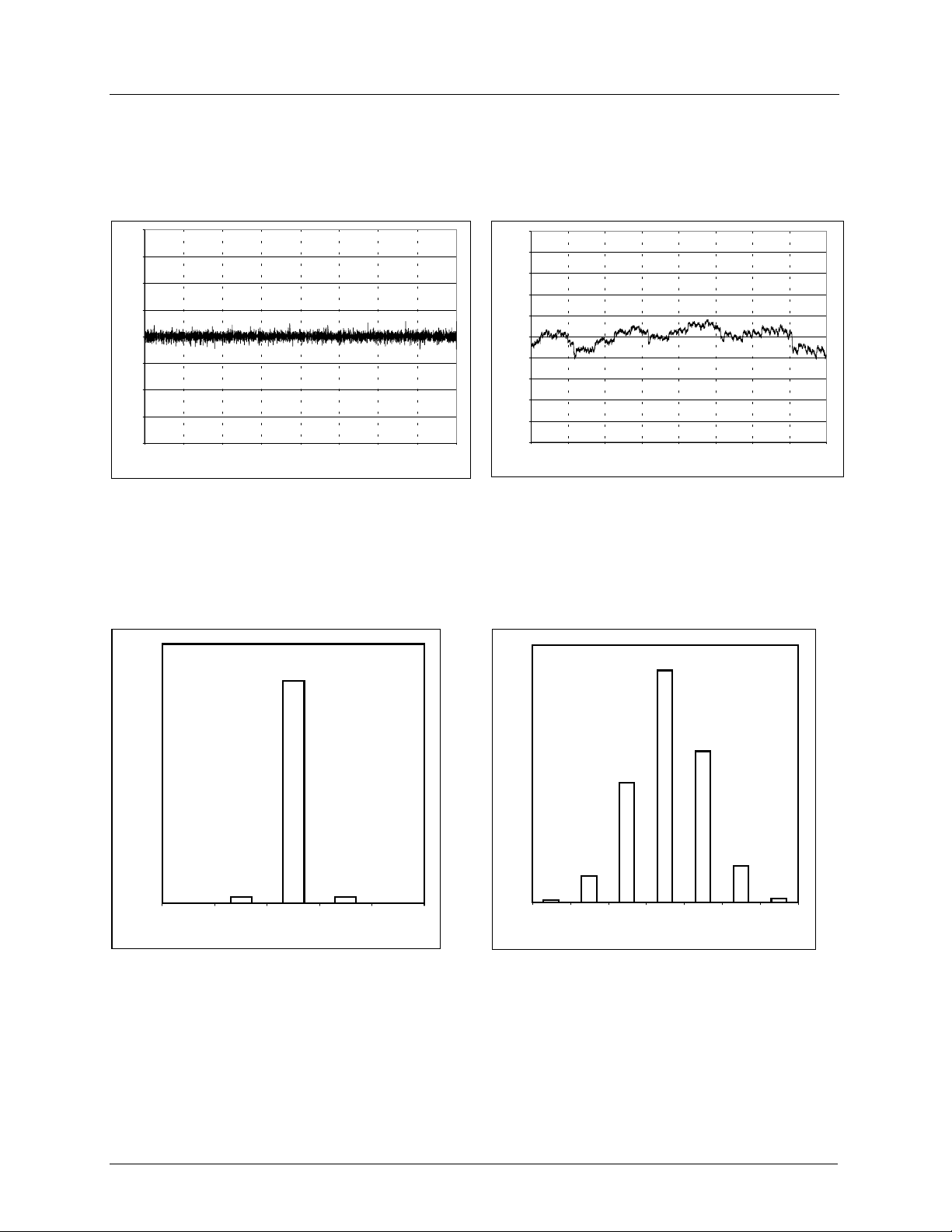
TYPICAL OVERALL SYSTEM PERFORMANCE
(INCLUDING CDS, PGA AND ADC BLOCKS) DNL VS CODES INL VS CODES
2
2
1.5
1.5
1
1
0.5
0.5
0
0
DNL (LSB's)
DNL (LSB)
-0.5
-0.5
-1
-1
-1.5
-1.5
-2
-2
0 512 1024 1536 2048 2560 3072 3584 4096
0 512 1024 1536 2048 2560 3072 3584 4096
Output Data Codes
Output Data Codes
5.00
5.00
4.00
4.00
3.00
3.00
2.00
2.00
1.00
1.00
0.00
0.00
INL (LSBs)
-1.00
INL (LSB)
-1.00
-2.00
-2.00
-3.00
-3.00
-4.00
-4.00
-5.00
-5.00
0 512 1024 1536 2048 2560 3072 3584 4096
0 512 1024 1536 2048 2560 3072 3584 4096
Output Data Codes
Output Data Codes
Production Data
Figure 9 DNL Vs Output Data Codes
(MODE 1, MCLK = 32MHz, AVDD = 5V, DVDD = 3.3V)
GROUNDED-INPUT HISTOGRAMS
1
RMS noise = 0.26 LSB
1
1
HITS (percent)
(of 262144 total)
0
0
0.00%
0
N-2 N-1 N N+1 N +2
2.85%
94.36%
2.79%
Output Data Code
0.00%
Figure 10 INL Vs Output Data Codes
(MODE 1, MCLK = 32MHz, AVDD = 5V, DVDD = 3.3V)
40.57%
RMS noise = 0.95 LSB
)
20.90%
of 262144 total
HITS (percent)
(
4.58%
0.40%
N-3 N-2 N-1 N N+1 N+2 N+3
Output Data Code
26.49%
6.34%
0.63%
Figure 11 Unity Gain Histogram
(MODE 1, MCLK = 32MHz, GAIN = 1, AVDD = 5V,
DVDD = 3.3V)
WOLFSON MICROELECTRONICS LTD
Figure 12 Maximum Gain Hi stogram
(MODE 1, MCLK = 32MHz, GAIN = 7.4, AVDD = 5V,
DVDD = 3.3V)
PD Rev 4.0 April 1999
13
Page 14
WM8148
SYSTEM INFORMATION
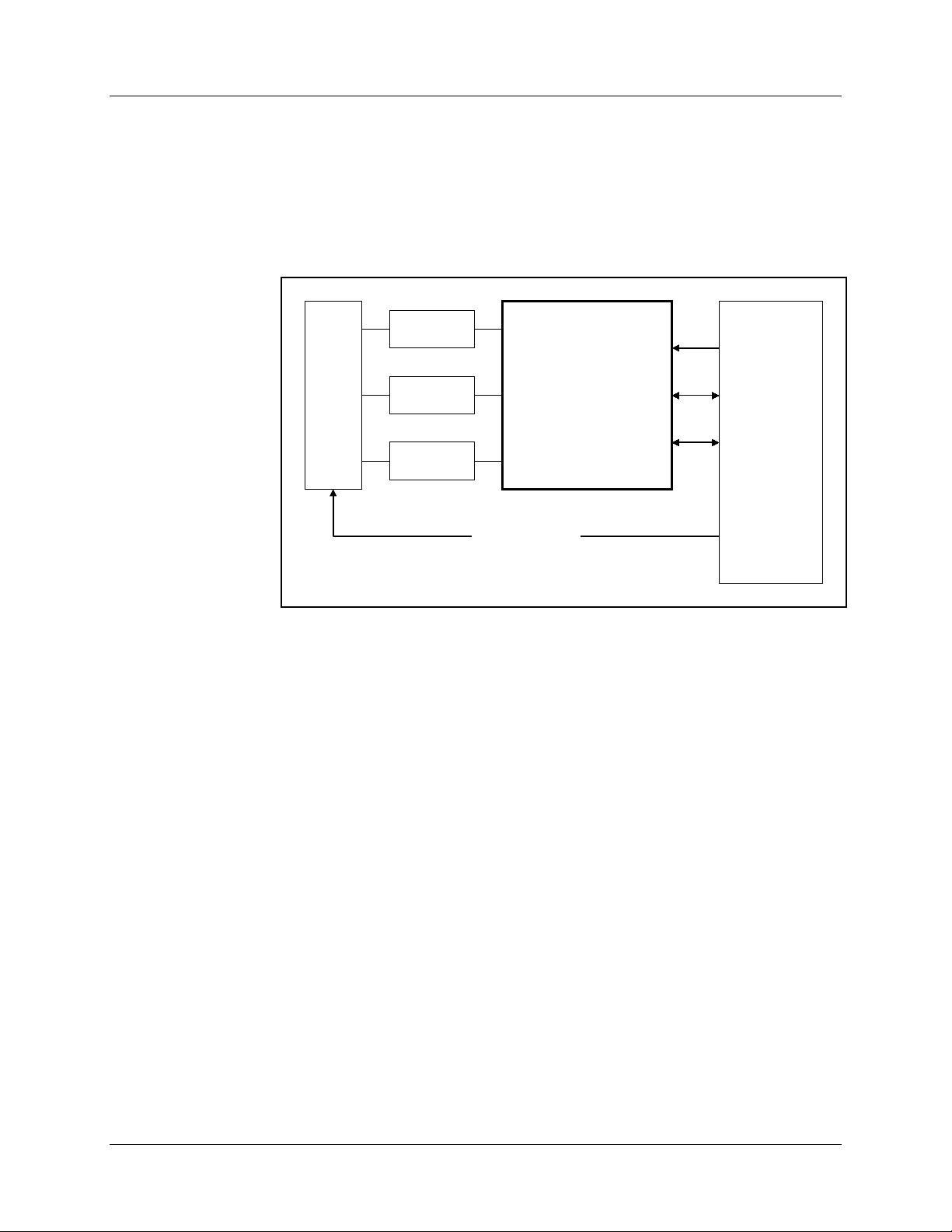
Figure 13 shows a system block diagram for a typical application. The CCD image sensor c ontains
three parallel linear arrays of sens or elements (sensitive to Red, Green, and Blue light respectively).
The Red, Green and Blue output signals are eac h applied to t he RINP, GINP and B INP channel i nputs
respectively of the WM8148. Each of t hese channels provide gain adjust, f or compensation of sens or
sensitivity and offset adjust for nulling out d.c. offset voltages . The outputs of t hese three channels are
time multipl exed into a single 12-bit resolution ADC. The digit al output is then transferred to a digit al
ASIC or other digital processor. The corrected data can then be c ompressed if required before being
output to a data storage device or a monitor.
Production Data
R
BUFFER
S
E
N
G
S
BUFFER
O
R
B
Figure 13 System Diagram
BUFFER
RINP
GINP
WM8148
BINP
SENSOR TIMING
CLOCKS
DATA
CONTROL I/F
SYSTEM
ASIC
WOLFSON MICROELECTRONICS LTD
PD Rev 4.0 April 1999
14
Page 15
WM8148
DEVICE DESCRIPTION
INTRODUCTION
The WM8148 samples up to three analogue inputs simultaneously, conditions these signals and
converts each resulting analogue signal to a 12-bit digital word.
A block diagram is s hown on page 1. Each of t he three input c hannels c onsist s of an Input Sam pling
block (CDS/RLC), an 8-bit programmable Offset DAC, and a 6-bit Programmable Gain Amplifier
(PGA). The outputs from the three channels are mult i pl exed into a 12-bit ADC. The digital output from
the ADC is presented on a 12-bit wide bi-direc t i onal bus.
A high-speed (up to 48MHz) master cl ock, MCLK, and a per-pixel sync hroni sation pulse, VS MP, drive
a shared Timing Control block to generate input sampling signals and other internal clocks.
Alternatively the device can operat e from MCLK only, output ting VS MP synchronis ation pulses to t he
rest of the system.
An internal reference provides buffered voltages VRT, VRB and VRX. A 4-bit DAC (RLC DAC)
provides a programmable buffered voltage at pin VRLC for us e as an input signal reference l evel or
an input clamp voltage.
The operation of the device is controlled by internal control regist ers, which can be read from and
written to via a Digital Management I nterface (DMI) in either serial or parallel mode.
INPUT SAMPLING
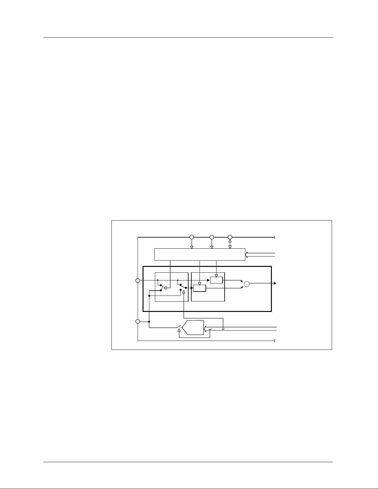
Figure 14 shows the configuration of t he Input Sampling Block for the red channel. (The green and
blue channels are the same. )
Production Data
MCLK VSMPRLC
RINP
VRLC
TIMING CONTROL
CL
RLC CDS
R
S/H
MODE[0]
4-BIT
RLC DAC
S
V
S/H
S
+
+
-
INPUT SAMPLING
BLOCK FOR RED
CHANNEL
From Control Interface
To Offset DAC
From Control Interface
Figure 14 Input Sampling Block – Configuration for Red Channel
This block contains switches to perform Reset Level Clamping (RLC) and Correlated Double
Sampling (CDS). Sample/Hold blocks sample the video and reset/reference levels of the input
waveform, and pass the diff erence signal on to the rest of the channel. Int ernal clocks V
and R
S
define the timing of t he sam pling of t he video signal and t he reset/ reference level respec tively. W hen
enabled by control input pin RLC, internal signal CL c lamps the input pin RINP to the volt age on pin
VRLC, which is driven either externally or from the 4-bit RLC DAC.
The detailed timing of t he internal cloc k signals CL, V
, and RS, with respect to VSMP and MCLK, is
S
controlled by the Timing Cont rol bl ock as programmed via the Di gi tal Management Interface (DMI).
S
WOLFSON MICROELECTRONICS LTD
PD Rev 4.0 April 1999
15
Page 16
WM8148
Production Data
INPUT SAMPLING MODES
To suit different sensors and applications, the W M8148 can sample one, two, or three channels
simultaneously, at t he rate of the VSMP clock. In each case there are two possible rati os of VSMP
frequency to the MCLK master clock frequency, and a choice of whether to use CDS. Table 1
summarises the options available, including the respective maximum sample rates. The mode of
operation is set by the Control Register bits MODE[3:0] as shown. Note MODE[0] def ines whether or
not CDS is activated.
MAX
SAMPLE
RATE PER
CHANNEL
(VSMP)
MSPS MHz MSPS CDS NON-
Three-channel
4 8 32 12 0 1
(8-phase)
Three-channel
412481289
(12-phase)
Two-channel
5.33 6 32 10.66 4 5
(6-phase)
Two-channel
6 8 48 12 12 13
(8-phase)
One-channel
6.66 6 40 6.66 2 N/A
CDS
One-channel
10 4 40 10 N/A 3
non-CDS
Table 1 Modes of Operation
If an external VSMP signal is not available, the WM8148 can be configured to output a
synchronisation pulse to t he system by setting control bi t FREE. The internally generated signal is
presented on the VSMP and/or SDO pins depending on the set tings of the cont rol bit s V SMPOP and
SDO[1:0].
CORRELATED DOUBLE SAMPLING (CDS)
The input signal can be sam pl ed i n t wo ways: Correlat ed Doubl e S ampling (CDS), or non-CDS.
MCLK/VSMP
FREQUENCY
RATIO
MAX MCLK
FREQENCY
MAX
OUTPUT
RATE
MODE
NUMBER
(MODE[3:0])
CDS
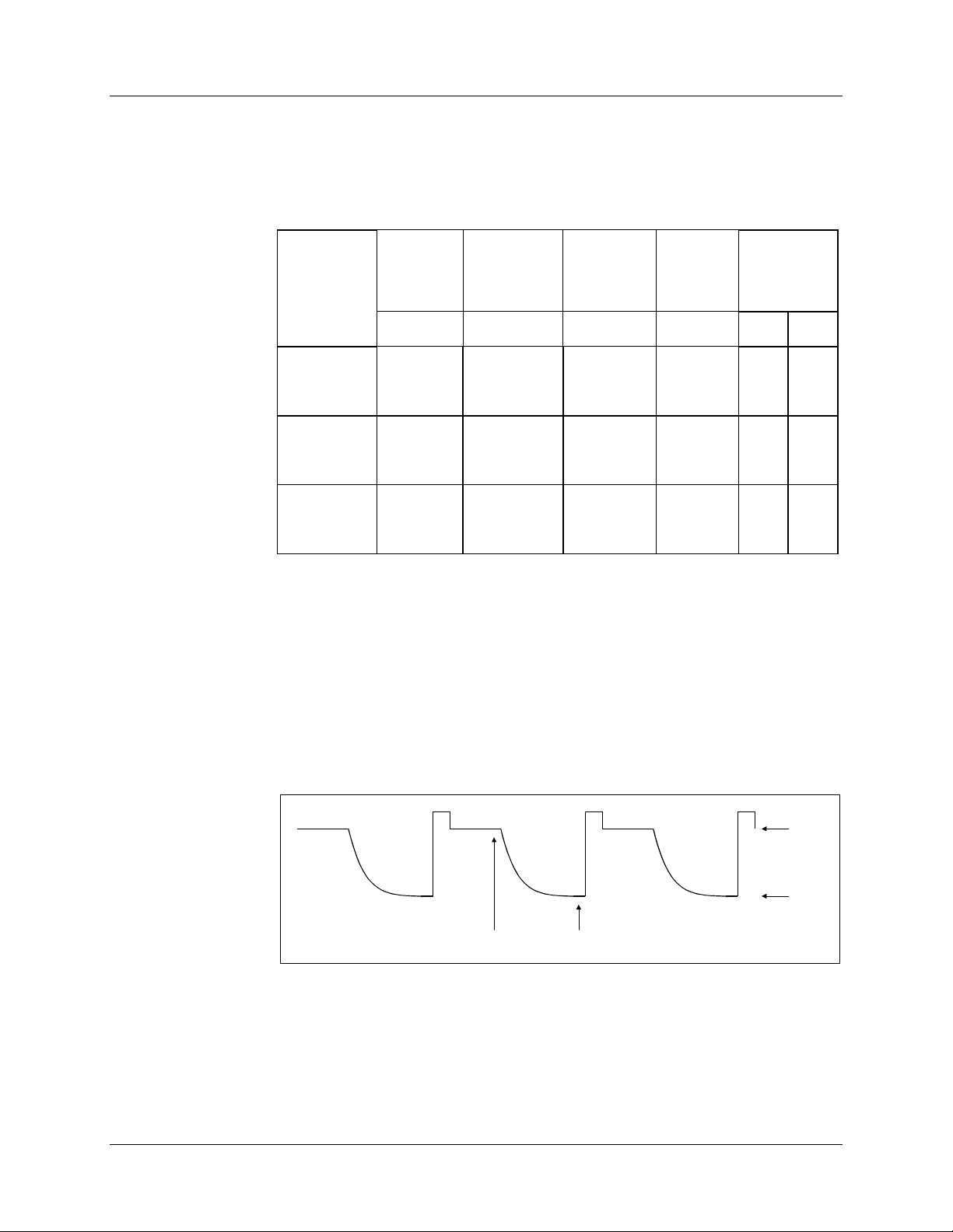
CDS operation is summ ari sed in Fi gure 15. The video s ignal proc ess ed is t he diff erence bet ween the
voltage applied at the RINP input when R
off, i.e. the difference between reset and video levels from the same pixel of the input signal. This
method of sampli ng i s recommended as it removes common-mode noise.
Figure 15 CDS Reset and Video Level Sampling
In non-CDS modes, R
the reference level applied to the V RLC pin. The video signal processed is the diff erence between
these samples (V
the RLC DAC. In these modes d.c. variations of t he i nput signal are not rejected.
WOLFSON MICROELECTRONICS LTD
turns off and the voltage at t he RINP input when VS turns
S
R
S
and VS occur simultaneous ly. VS samples the video s ignal, while RS samples
S
). The voltage (V
RS-VVS
VRLC
V
S
), on pin VRLC, may be driven externally or internall y by
PD Rev 4.0 April 1999
V
RS
V
VS
16
Page 17
WM8148
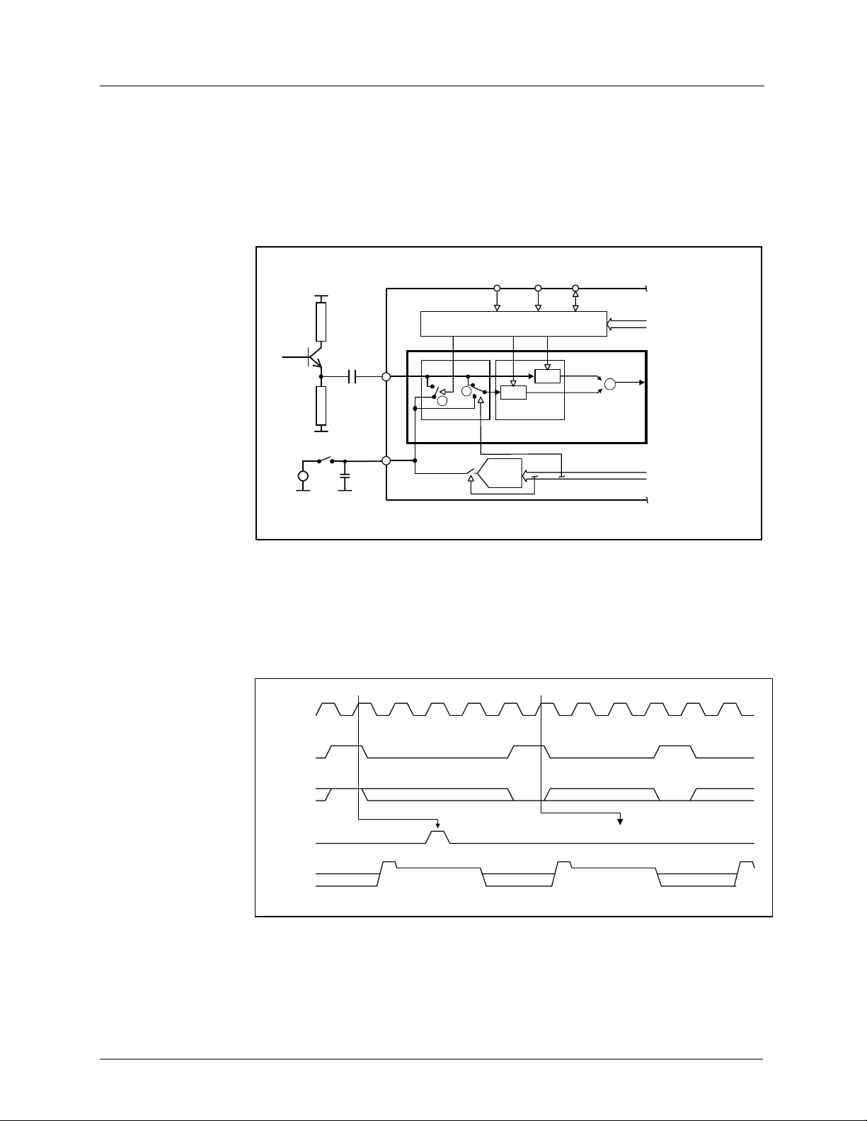
RESET LEVEL CLAMPING (RLC)
If the sensor output volt age is within t he input range of t he W M8148, the s ensor may be d. c. c oupled
into the WM8148 either directly or via a buffer. If t he output from t he sens or is outs ide t he input range
of the WM8148, the s i gnal has to be connected via a c apacitor, C
be defined on the WM8148 side of the capacitor (at RINP).
Setting of the d.c. bias conditi ons is best performed by Reset -Level Clamping, activated by pin RLC.
Reset-Level Clamping is compatible with both CDS and non-CDS operating modes. A typical
configuration is shown in Figure 16.
Production Data
, and the d.c. bias condi tions m us t
IN
MCLK VSMPRLC
C
IN
RINP
EXTERNAL VRLC
VRLC
TIMING CONTROL
CL
2
1
RLC CDS
4-BIT
RLC DAC
R
S/H
MODE[0]
V
S
S
S/H
+
+
-
INPUT SAMPLING
BLOCK FOR RED
CHANNEL
FROM CONTROL
INTERFACE
TO OFFSET DAC
FROM CONTROL
INTERFACE
Figure 16 Reset-Level Clamping Circuitry
When the clamp pulse, CL, is active, the voltage on the W M8148 side of C
equal to the VRLC voltage, V
initially remain at V
of C
will couple through CIN to RINP. Switch 2 determ ines whether the RS level is taken from the
IN
, but any subsequent variation in s ensor voltage appearing at the sensor si de
VRLC
, by switch 1. When the CL pulse turns off, the RINP voltage will
VRLC
, at RINP, will be forced
IN
incoming signal (CDS operat i on) or the VRLC pin (non-CDS operation).
Figure 17 demonstrates t he case of a typical CCD waveform, with CL applied duri ng the reset period.
MCLK
VSMP
RLC
Input Video
Figure 17 Relationship of RLC pin, MCLK and VSMP to Internal Clamp Pulse, CL
The input signal applied to the RLC pin is sampl ed on the positive edge of MCLK that occurs during
each VSMP pulse. The sampled l evel, high (or low) control s t he presenc e (or absenc e) of t he int ernal
CL pulse on the next reset level. The position and duration of CL is adjustable by control bits
RESREF[3:0] and SMALL.
WOLFSON MICROELECTRONICS LTD
1XX XX00X
Programmable Delay
CL
r,g,br,g,br,g,b
RLC on this pixel No RLC on this pixel
PD Rev 4.0 April 1999
17
Page 18
WM8148
If pin RLC is tied high then reset level clamping is appli ed on every pixel. Alternatively, for line-byline clamping, pin RLC can be driven high at the start of a line (during the dum m y black pixel output ),
then driven low for the remainder of the line. If pin RLC is t i ed low then reset level clamping will not be
applied.
The VRLC voltage, to which the reset level is clamped, can be defined either by an external volt age
or internally via the 4-bit program m able RLC DA C. To c lamp to an internally defi ned vol tage RLCE XT
must be set to ‘0’. Control bit s RLCV[3:0] then program the RLC DAC to a voltage ranging bet ween
0V and AVDD linearly over 15 steps. The voltage from the RLC DAC will also be presented on pin
VRLC which should be decoupled to analogue ground. Alternatively, by setti ng control bit RLCEXT to
‘1’, the RLC DAC is disconnected and the VRLC pin is driven externally t o any voltage between 0V
and AVDD.
PROGRAMMABLE OFFSET DAC
The output from the Input Sampling Block is added to the output of an 8-bit Offset DAC to allow
cancellation of offsets in sensor black level and input offsets of the WM8148. The DACs cover a
range of ±200mV in 255 equal steps of 1.57mV, programm able via t he DMI. Program mi ng 00(hex) to
the DAC gives an offset adj us tment of -200mV, FF(hex) adjusts the input signal by +200mV.
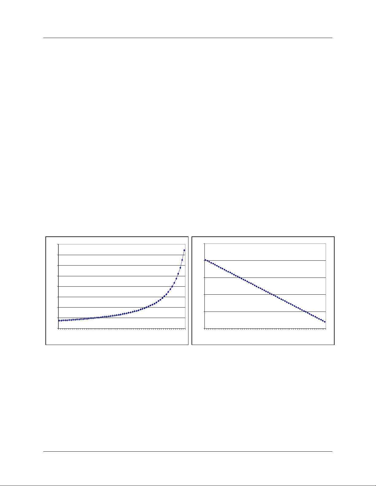
PROGRAMMABLE GAIN AMPLIFIERS (PGA)
When the black level has been adjusted using the Offset DAC, the gain of the PGA can be
programmed to ampli fy the white level signal to cover the full ADC range (3V ). Figure 18 shows a
graph of the PGA gain response. Thi s gain curve is non-linear, with gain given by:
Gain = 52 / {70 – PGA[5:0](dec)}
This gives a gain ranging from 0.74 times to 7.4 times over 63 steps, with minimum gain
corresponding to 00(hex) and maximum gain c orresponding to 3F(hex). Figure 19 shows the PGA
gain code settings required, f or PGA input voltages from 0.4V to 4.0V, to produce a PGA output
equivalent to the full sc al e i nput range of the ADC (3V).
Production Data
8
7
6
5
4
Gain
3
2
1
0
000306
121518
09
0F
0C
PGA Gain code, PGA[5:0] (hex)
1B
1E
212427
2A
303336
2D
39
3C
5
4
3
2
PGA Input Voltage (V)
1
0
3F
000306
09
121518
0F
0C
PGA Gain code, PGA[5:0] (hex)
1B
1E
212427
2A
2D
303336
39
3F
3C
Figure 18 PGA Gain Response Figure 19 PGA Input vs Gain Code for Full Scale ADC Input
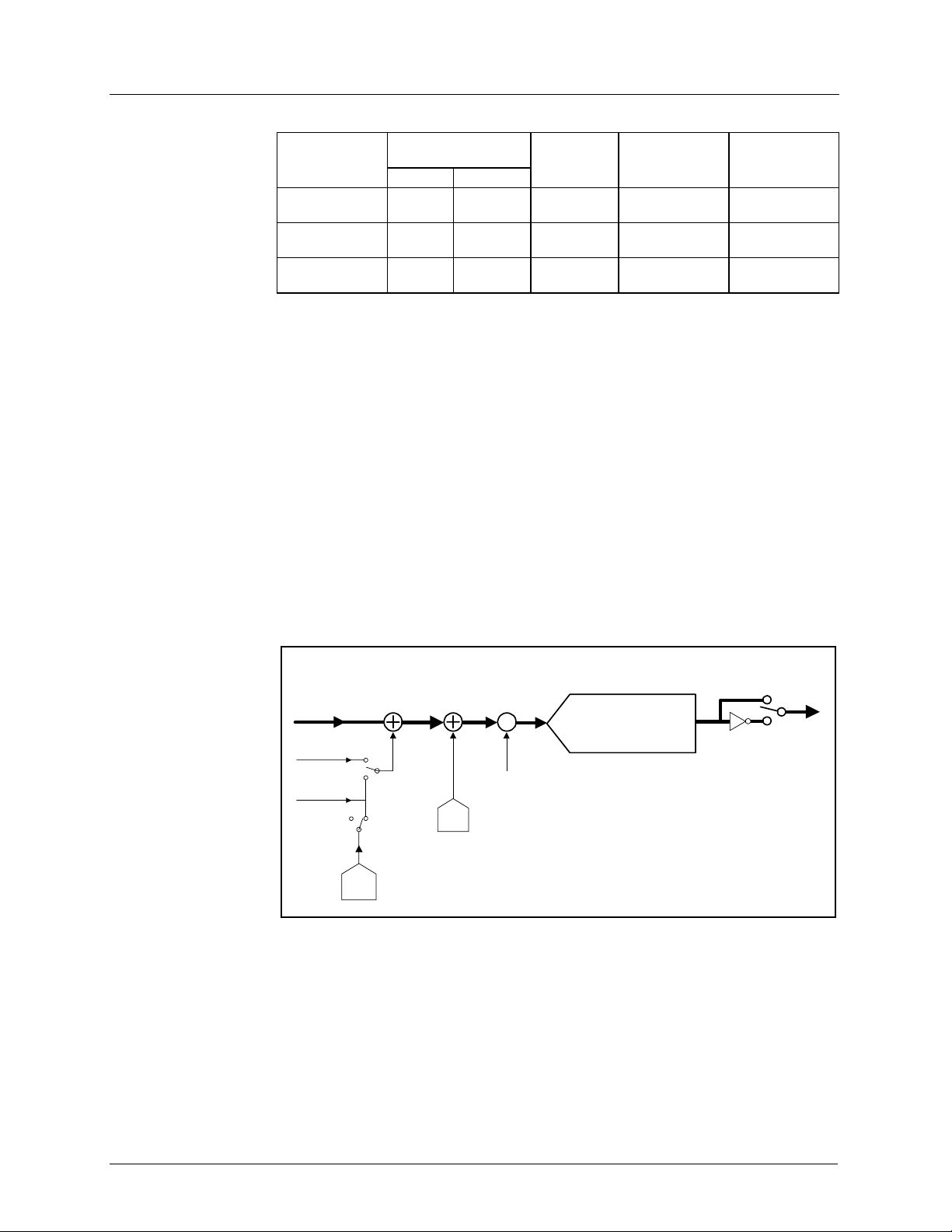
ANALOGUE TO DIGITAL CONVERTER (ADC)
The output of the PGA is appl ied to a high performance ADC. The differential signal from the PGA
ranges from 0V (black l evel) to either +3V or -3V (white level), depending on the polarity of the input
signal to the device. Control bi ts PGAFS[1:0] are us ed t o configure the input of the ADC to accept the
desired input signal range. This is achieved by adding 0, + or - half of the full s cale voltage to the
ADC input signal on a channel-by-channel bas is, as shown in the bloc k diagram on page 1. Table 2
shows the PGAFS[1:0] settings required for different vi deo signal types.
WOLFSON MICROELECTRONICS LTD
PD Rev 4.0 April 1999
18
Page 19
WM8148
Production Data
VIDEO SIGNAL
TYPE
BLACK WHITE
Positive-going,
e.g. many CIS
Negative-going,
e.g. CCDs
Bipolar -1.5V +1.5V 00, 01 Black = 0
Table 2 PGAFS[1:0] Setting for Video Signal Types
If the signal exceeds the chos en range, it is cl ipped and the error flag OVRNG is s et, which m ay be
output via the SDO or OP pins.
OVERALL SIGNAL FLOW SUMMARY
Figure 20 represents the processi ng of the video signal through the WM8148.
The
INPUT SAMPLING BLOCK
difference between the input video l evel V
difference between the input video level V
the RLC DAC.
The
OFFSET DAC BLOCK
black level of the input s i gnal towards 0V, producing
The
PGA BLOCK
outputting voltage
then amplifies the white level of the input signal to maximise the ADC range,
.
V
3
DIFFERENTIAL
SIGNAL RANGE
PGAFS[1:0] OUTPUT CODE
INVOP = 0
0V 3V 11 Black = 0
White = 4095
0V -3V 10 B l ac k = 4095
White = 0
OUTPUT CODE
INVOP = 1
Black = 4095
White = 0
Black = 0
White = 4095
Black = 4095
White = 4095
produces an effective input voltage
and the input reset level V
IN
and the voltage on the VRLC pin, V
IN
RESET
. For CDS, this is the
V
1
. For non-CDS this is the
White = 0
, optionally set via
VRLC
then adds the amount of fine offset adjustment required to move the
.
V
2
The
ADC BLOCK
then converts the analogue signal,
V
The digital output is then inverted if required, through the
INPUT
V
IN
MODE[0] = 0
V
RESET
MODE[0] = 1
V
VRLC
RLCEXT=1
SAMPLING
BLOCK
V
+
-
RLCEXT=0
RLC
AVDD*RLCV[3:0]/15
DAC
OFFSET DAC
BLOCK
1
+
+
Offset
DAC
PGA
BLOCK
V
V
2
A = 52/(70-PGA[5:0])
200mV*(DAC[7:0]-127.5)/127.5
3
X
analog
PGA gain
+0 codes if PGAFS[1:0]=11
+4095 codes if PGAFS[1:0]=10
+2047 codes if PGAFS[1:0]=0x
Figure 20 Overall Signal Flow
, to a 12-bit unsigned digital output,
3
OUTPUT INVERT BLOCK
ADC BLOCK
x 4095/VFS) =
V
3
V
is RINP or GINP or BINP
IN
is VIN sampled during reset clamp
V
RESET
VRLC is voltage applied to VRLC pin
MODE[0], RLCEXT,RLCV[3:0], DAC[7:0],
PGA[5:0], PGAFS[1:0] and INVOP are set
by programming internal control registers.
MODE[0]=0 for CDS, 1 for non-CDS
to produce
OUTPUT
INVERT
BLOCK
D
1
digital
D2 = D1 if INVOP = 0
D2 =4095-D1 if INVOP = 1
.
D
1
D
2
D
2
OP[11:0]
.
WOLFSON MICROELECTRONICS LTD
PD Rev 4.0 April 1999
19
Page 20

WM8148
Production Data
CALCULATING OUTPUT FOR ANY GIVEN INPUT
The following equations describe the processing of the video and reset level signals through the
WM8148.
INPUT SAMPLING BLOCK: INPUT SAMPLING AND REFERENCING
If MODE[0] = 0, (i.e. CDS operation) the previously s ampled reset level, V
, is subtracted from
RESET
the input video.
1
=VIN - V
V
Eqn. 1
RESET
If MODE[0] = 1, (non-CDS operation) t he sim ultaneous ly sam pled volt age on pi n VRLC is subtract ed
instead.
V
1
If RLCEXT = 1, V
If RLCEXT = 0, V
V
VRLC
=VIN - V
is an externally applied voltage on pin VRLC.
VRLC
is the output from the internal RLC DAC.
VRLC
= AVDD ∗ RLCV[3:0] / 15 Eqn. 3
Eqn. 2
VRLC
OFFSET DAC BLOCK: OFFSET (BLACK-LEVEL) ADJUST
The resultant signal
V
2
is added to the Offset DA C output.
V
1
=
+ 200mV ∗ (DAC[7:0]-127.5) / 127. 5 Eqn. 4
V
1
PGA NODE: GAIN ADJUST
The signal is then mult i pl i ed by the PGA gain,
=
V
3
∗ 52/(70- PGA[5:0]) Eqn. 5
V
2
ADC BLOCK: ANALOGUE-DIGITAL CONVERSION
The analogue signal is then converted to a 12-bit unsigned number, with input range configured by
PGAFS[1:0].
[11:0] = INT{ (
D
1
[11:0] = INT{ (
D
1
/VFS) ∗ 4095} + 2047 PGAFS[1:0] = 00 or 01 Eqn. 6
V
3
/VFS) ∗ 4095} PGAFS[1:0] = 11 Eqn. 7
V
3
where the ADC full-scale range, V
OUTPUT INVERT BLOCK: POLARITY ADJUST
The polarity of the digital output may be inverted by control bit I NVOP.
OUTPUT DATA FORMAT
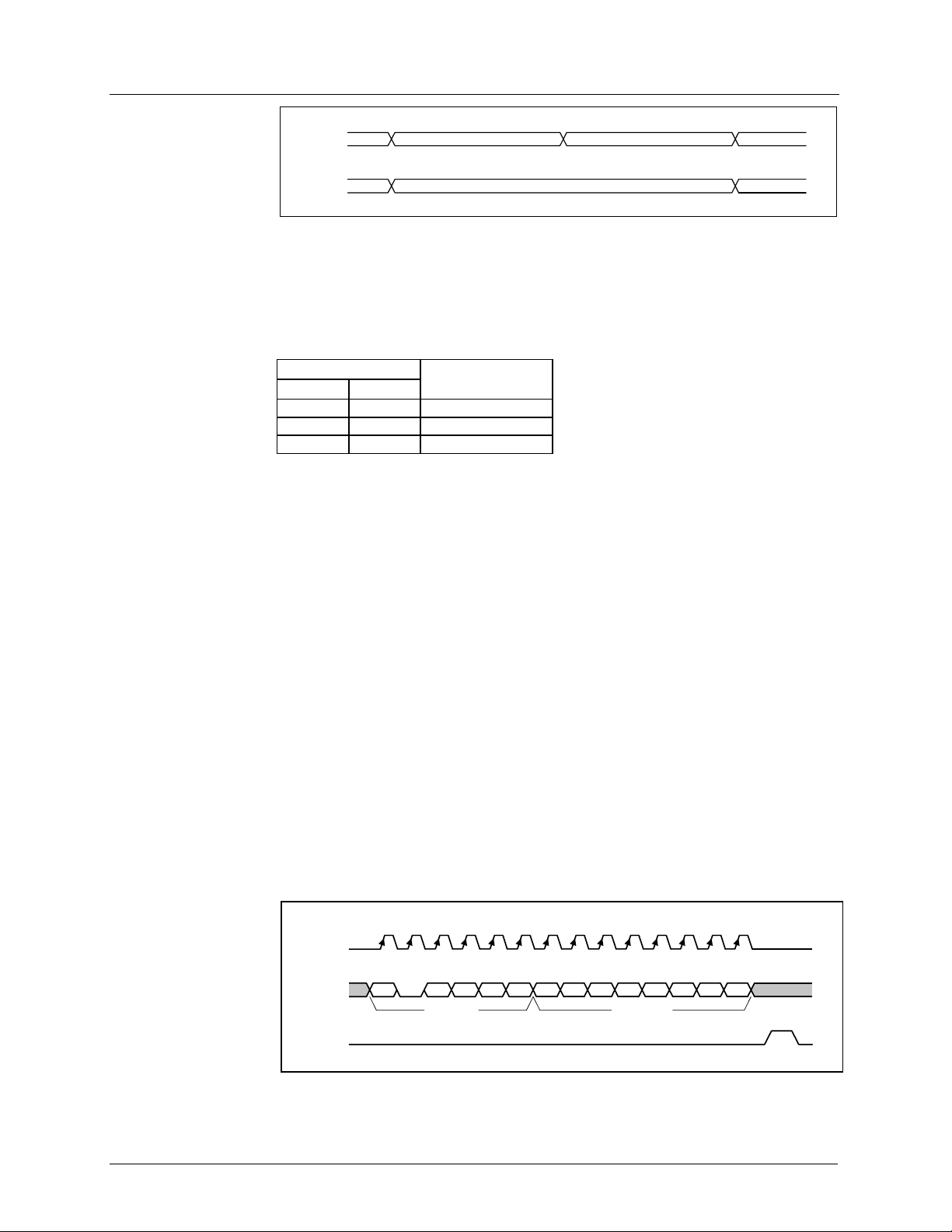
MULTIPLEXED AND NON-MULTIPLEXED OUTPUT FORMAT
Data is output from t he devic e, by def ault, as a 12-bi t wide word on OP [11: 0]. The out put changes on
every Nth negative-going edge of MCLK where N = 2, 4, or 6 according to the video sampling m ode.
This is shown as byte C in Figure 21.
If control bit MUXOP is set hi gh, data is output in a 2 x 8-bit word format , with data c hanging every
Nth negative-going edge of MCLK, where N = 1, 2, or 3 according t o video sampling mode. This is
shown as bytes A and B in Figure 21. Data is presented on pins OP [11:4] at twice the output pixel
rate. Bits CC[1] and CC[ 0] are us ed to i ndicat e which channel the A DC input was t aken f rom . Table 3
shows the channels corresponding to the CC[1:0] bit values. Bits TVIOL and OVRNG of byte B are
Error Flags, these are descri bed bel ow.
WOLFSON MICROELECTRONICS LTD
[11:0] = INT{ (
D
1
[11:0] =
D
2
D
2
D
[11:0] = 4095 –
/VFS) ∗ 4095} + 4095 PGAFS[1:0] = 10 Eqn. 8
V
3
, = 3V.
FS
[11:0] (INVOP = 0) Eqn. 9
1
[11:0] (INVOP = 1) Eqn. 10
D
1
PD Rev 4.0 April 1999
20
Page 21
WM8148
Production Data
OP[11:4]
MUXOP=1
OP[11:0]
MUXOP=0
C
BA
Figure 21 Output Data for 2 x 8-bit and 12 bit Output.
Where:
A = < d11, d10, d9, d8, d7, d6, d5, d4 >
B = < d3, d2, d1, d0, TVIOL, CC[1], CC[0], OVRNG >
C = < d11, d10, … d1, d0 >
COLOUR CODE BITS
CHANNEL
CC[1] CC[0]
00 Red
0 1 Green
10 Blue
Table 3 Colour Code Bits CC[1:0]
ERROR FLAGS
The two error flags are:
This goes high if the reset sample and clamp positions set up in bits RESREF[3:0], are
TVIOL:
inconsistent with the s el ected mode of operation.
OVRNG:
This goes high if the input t o the ADC exceeds its input range.
These flags are output in byte B of multiplexed-mode parallel output data as above. Each is also
available via the SDO pin if so c onfigured via the SDO[1:0] register bi ts.
LATENCY
Default latency from the last ris ing edge of MCLK during the VS MP pulse to data output depends on
the chosen Input Sampling Mode. To al ign pixel outputs with post proc essing circuit ry and to reduce
interaction with video sampling instances, the latency through the W M8148 device can be adjusted
by Control bits DEL[1:0] and FDEL[1:0].
DIGITAL MANAGEMENT INTERFACE (DMI)
The DMI is used to write contents to and read back contents from the i nternal regi st ers i n either s erial
or parallel mode. The PNS pin is tied low for serial and high for parallel mode.
SERIAL INTERFACE
REGISTER WRITE
SCK
SDI
SEN
a5 0 a3a2a1a0b7b6b5b4b3b2b1b0
Address Data Word
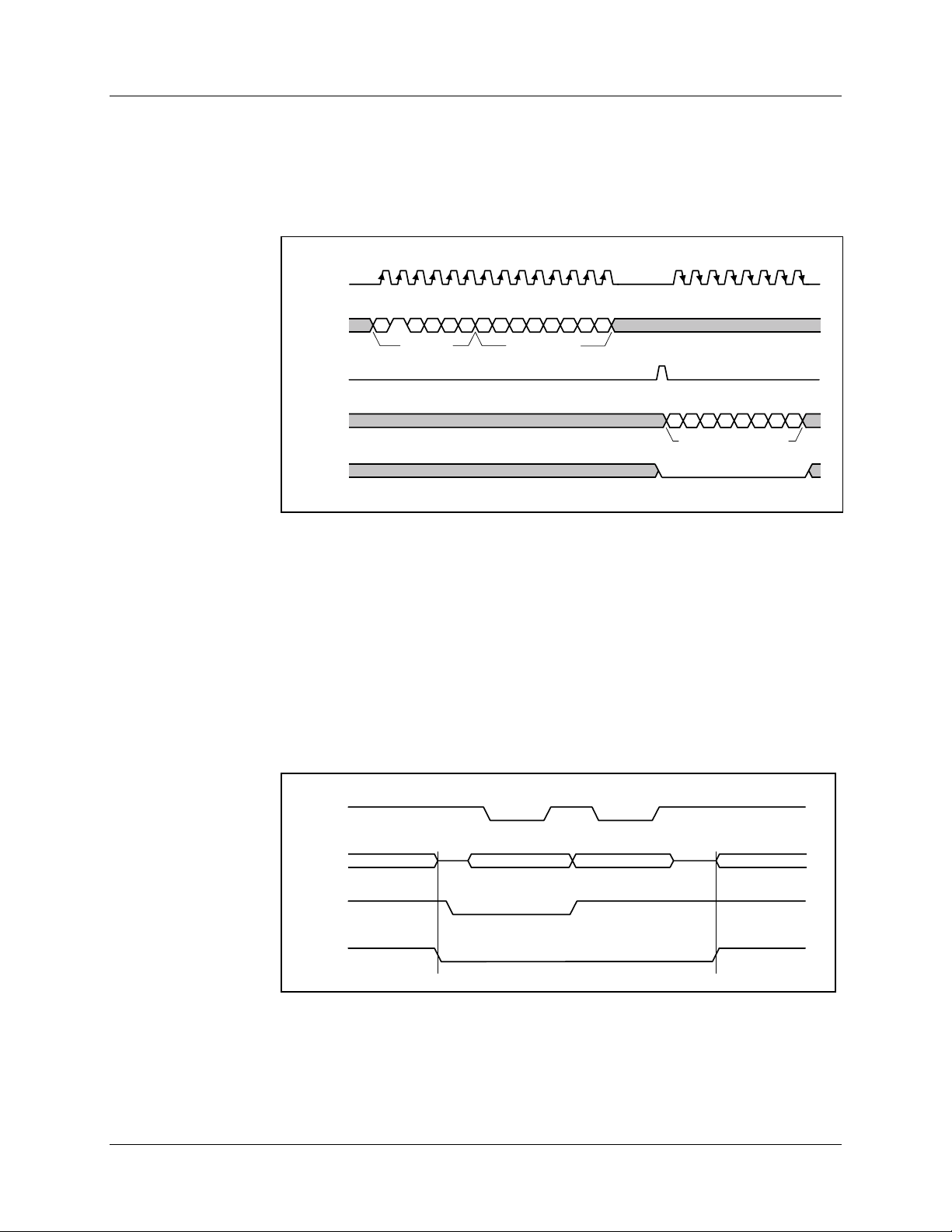
Figure 22 Serial Interface Register W rite
WOLFSON MICROELECTRONICS LTD
PD Rev 4.0 April 1999
21
Page 22
WM8148
Production Data
Figure 22 shows register writing in serial mode. Three pins, SCK, SDI and SEN are used. A six-bit
address (a5, 0, a3, a2, a1, a0) is clocked in through SDI, MSB first , f oll owed by an eight-bit dat a word
(b7, b6, b5, b4, b3, b2, b1, b0), also MSB first. Each bit is latched on the rising edge of SCK. W hen
the data has been shifted into the device, a pulse is applied to SEN to transfer the data
to the appropriate internal register. Note all valid registers have address bit a4 equal to 0 in
write mode.
REGISTER READ-BACK
SCK
Figure 23 Serial Interface Register Read-back
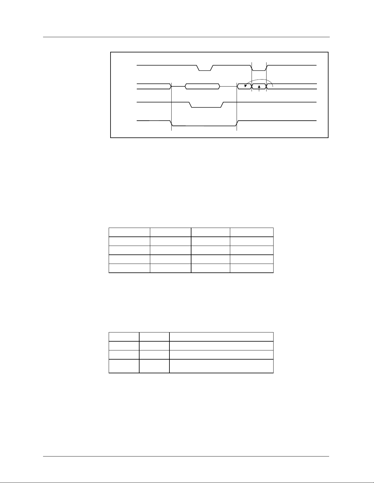
Register read-back is initiated by writing to the serial bus as described, but with address bit a4 set to
1, followed by an 8-bit dummy data word. Writing address (a5, 1, a3, a2, a1, a0) will cause the
contents (d7, d6, d5, d4, d3, d2, d1, d0) of corresponding regi ster (a5, 0, a3, a2, a1, a0) t o be out put
MSB first on pin SDO (on the falling edge of SCK), provided control bits S DO[1: 0] = 00. If SDO[ 1:0] is
not set to 00 then error flags will be output inst ead of the regist er contents . Note t hat if SDI and S DO
are not connected together, the next word may be read in to SDI while the previous word is s till being
output on SDO. Alternatively, the us er m ay ti e the S DI and SDO pi ns t ogether t o m ak e a 3-wire serial
interface. The user must ensure that the circui t dri vi ng S DI i s Hi-Z while the SDO pin is active.
Pin OEB must be low to enable the output data word to be output.
PARALLEL INTERFACE
REGISTER WRITE
SDI
SEN
SDO
OEB
a51a3a2a1a0xxxxxxxx
Address Data Word
d7 d6 d5 d4 d3 d2 d1 d0
Output Data Word
STB
OP[11:4]
DNA
RNW
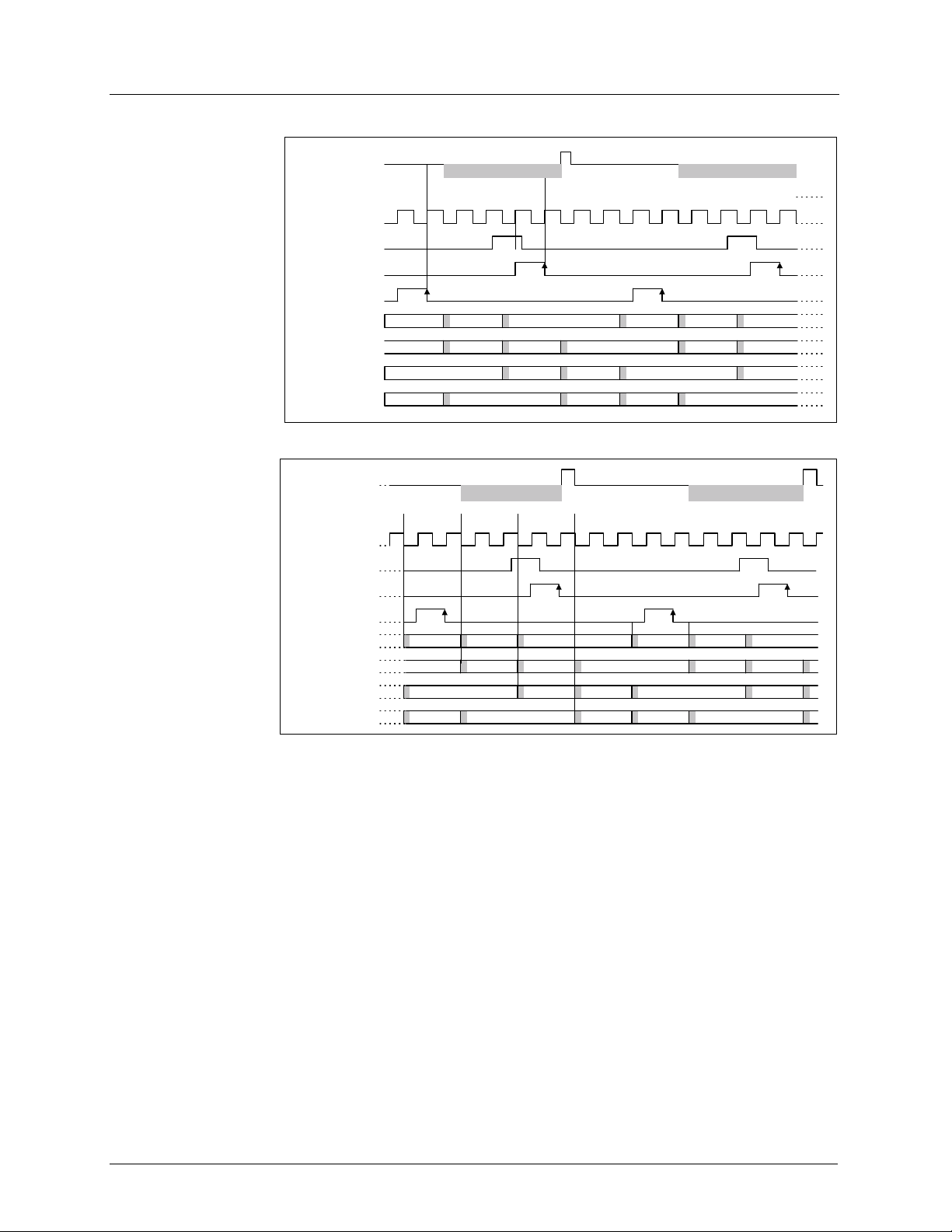
Figure 24 Parallel Interface Register Write
The parallel interface uses bi ts [11:4] of the OP bus and the STB, DNA and RNW pins. Pin RNW
must be low during a write operation. The DNA pin def ines whether the data byte i s address (low) or
data (high). The 6-bit address (a5, 0, a3, a2, a1, a0) is i nput into OP[9:4] , LSB into OP [4], (OP[10]
and OP[11] are ignored) when DNA is low, then the 8-bit data word is input into OP[11:4] , LSB int o
OP[4], when DNA is high. The data bus OP[11:4] f or both address and data is lat ched in during the
low period of STB. Note all valid registers have address bit a4 equal to 0.
WOLFSON MICROELECTRONICS LTD
Driven by WM8148
Normal Output Data
Hi-Z Hi-Z
Driven Externally
Address Data
Driven by WM8148
Normal Output Data
PD Rev 4.0 April 1999
22
Page 23
WM8148
Production Data
REGISTER READ-BACK
STB
OUTPUT ENABLE
Driven by WM8148
Normal Output Data
OP[11:4]
Driven by WM8148
Normal Output Data
Hi-Z
Driven Externally
Address
Hi-Z
Read Data
DNA
RNW
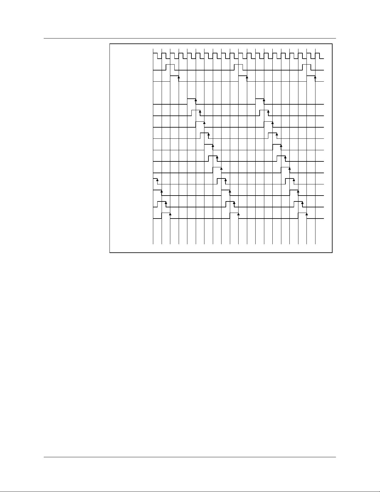
Figure 25 Parallel Interface Register Read-back
Register read-back is init iated by writing the 6-bit address (a5, 1, a3, a2, a1, a0) into OP[9:4] by
pulsing the STB pin low. Note that a4 = 1 and pins RNW and DNA are low. W hen RNW and DNA are
high and STB is strobed again, the c ontents (d7, d6, d5, d4, d3, d2, d1, d0) of the corres ponding
register (a5, 0, a3, a2, a1, a0) will be output on OP[11:4], LSB on pin OP[4]. Until STB is pulsed low,
the current contents of the ADC (shown as Normal Output Data) will be present on OP[11:4].
When high, pin OEB makes pins OP [11:0] Hi-Z regardless of other pin setti ngs. Therefore when the
WM8148 is outputting norm al ADC data, or during regist er read, pin OEB must be s et to ‘0’. During
register write, pin RNW set to ‘0’ ensures that the output s are Hi-Z, theref ore pin OEB is ‘ don’t care’.
Table 4 shows the state of pins OP [11:0] for possible set t i ngs of OEB, RNW and S T B .
OEB RNW STB OP[11:0]
1xxHi-Z
x0xHi-Z
0 1 0 Read register data
0 1 1 Read ADC dat a
Table 4 State of OP[11:0] During Register Read/Write
POWER MANAGEMENT
Power management for the WM8148 is performed via the DMI. The device can be powered on or off
completely by the control bit EN. Alt ernatively, when control bit S ELEN is high, only blo cks selected
by further control bits SENBL[7:0] are powered up. This al lows the user to opt im ise power dissi pation
in certain modes, or to define intermediate st andby modes to allow a quicker recovery into a fully
active state.
EN SELEN
00
10
x1
Table 5 Power Down control
Control bit RLCEXT is used to disable the RLC DAC, regardless of EN or SENB L[7: 0]. If thi s opt ion is
taken, pin VRLC can be driven externally for reset l evel clamping.
One-channel and Two-channel sampling m odes do not autom atically power down unused PGAs, the
appropriate SENBL bits should be set during initialisation to save power. The WM8148 will still
operate normally if the unused bl ocks are not powered down.
All the internal registers maintain their previous ly programmed value in power down modes, and t he
DMI inputs remain active.
WOLFSON MICROELECTRONICS LTD
Device completel y powers down.
Device completel y powers up.
Only blocks with respective SENBL bit high
go/remain active.
PD Rev 4.0 April 1999
23
Page 24

WM8148
REGISTER RESET
RESET ON POWER UP
To set the registers to t heir default values, pin NRESET must be held low during power-up. If pin
OVRD is also held low, all of the registers will be set to their default values including bits SELEN and
EN which will disable all of the analogue circuitry. If pin OVRD is held high during power up with pin
NRESET held low, all of the registers will be set to their default value with the exception of EN and
RLCEXT, which will enable all of the analogue circuitry in the device.
RESET DURING OPERATION
During device operation, pulsing NRESET low will reset all of the registers depending on the polarity
of the OVRD pin as above.
The registers may also be res et by writing to bits SRES[1: 0]. This allows reset of:
1) Only the PGA Gains and Offset DAC Values regis t ers,
2) All registers except power-management registers S ELEN, EN, and SENBL, or
3) All registers, equivalent to the NRESET function.
REFERENCE VOLTAGES
The ADC reference voltages are derived from an internal bandgap reference, and buffered to
pins VRT and VRB, where they must be decoupled to ground. Pin VRX is driven by a similar buffer,
and also requires decoupling. The output buffer from the RLC DAC also requires decoupling at
pin VRLC.
Production Data
Peak sink and source currents of the reference buffers are typically between ±1mA and ±6mA,
depending on output voltage and current polarity. This limits the slew-rate into the decoupling
capacitors on power-up. When disabled, the buffers become high-impedance (I < 1µA), so the
decoupling capacitor voltage will not drop much during short (< 100ms) disable durations .
DETAILED MODE TIMING DIAGRAMS
The following diagrams show Input Signal Sampling Diagrams, Output Data Timing and Reset
Sample/Clamp Positions for each mode of the WM8148.
INPUT SIGNAL SAMPLING DIAGRAMS
These diagrams show the required MCLK and VSMP (externally or internally generated) signals.
From these signals, internally generated signals V
levels (in CDS modes) respectively. In non-CDS modes, the reference level is sampled
simultaneously with V
from the sensor output waveform to the respec tive V
the arrow on the falling edge of the V
number of MCLK periods in total, and MCLK phase, which counts the number of MCLK periods
between each VSMP pulse. Note that the duration of the VSMP puls e must not include more than
one MCLK rising edge, as this will reset the phase timing. The output waveforms are included. The
position of the R
been included.
OUTPUT DATA TIMING DIAGRAMS
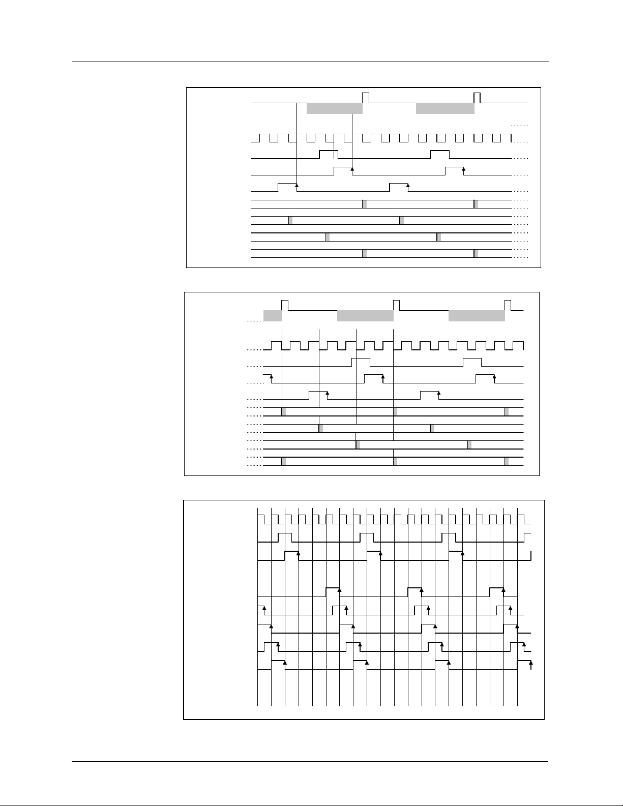
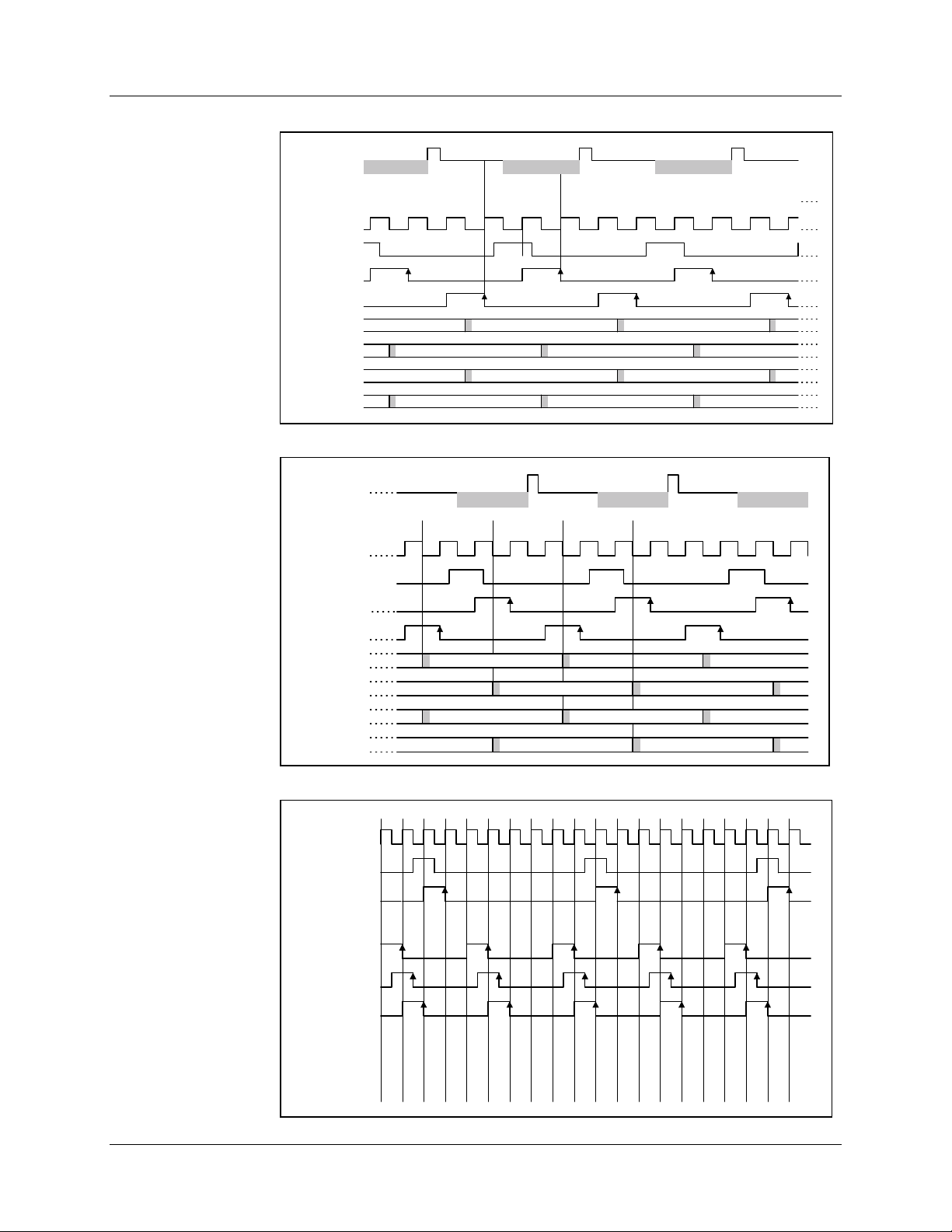
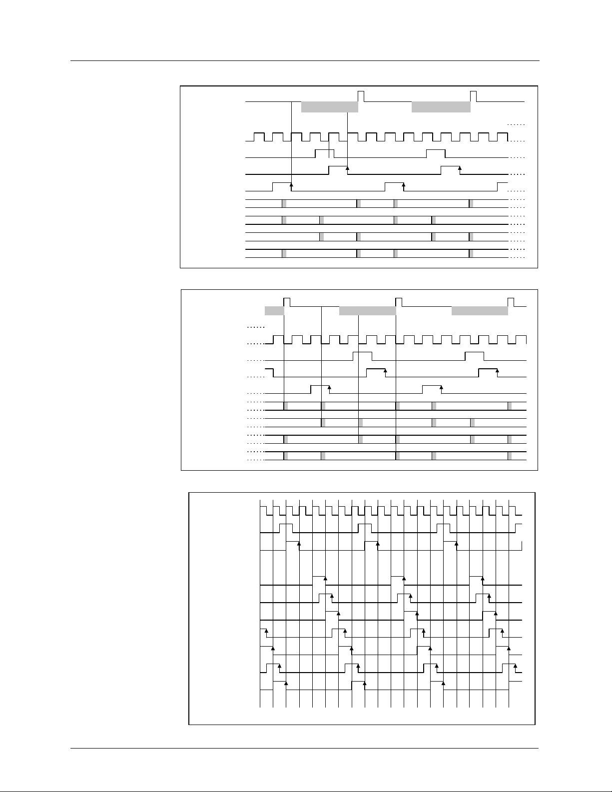
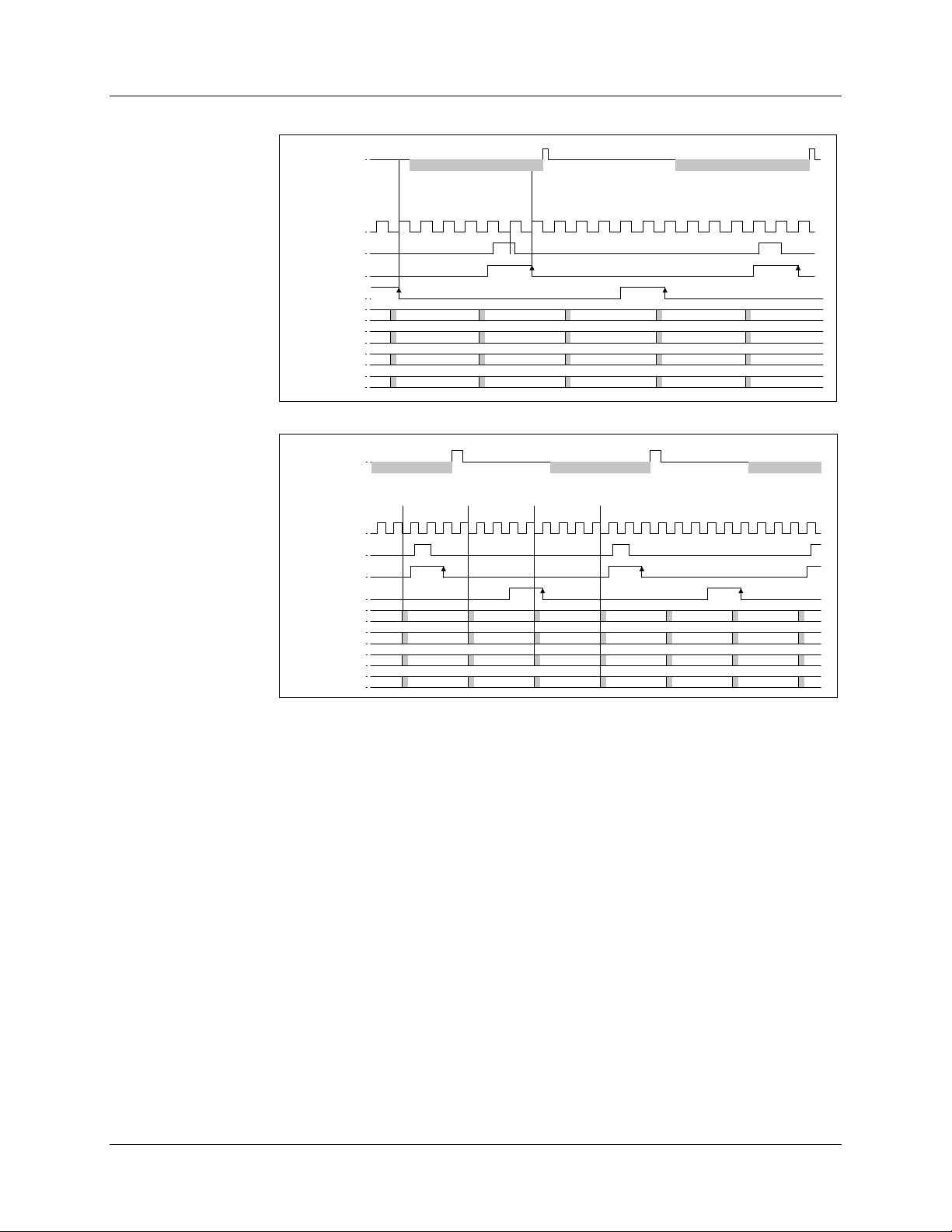
The output timing diagrams are used to calculate t he latency through t he device, which is dependent
on the operating mode. The latency can be programmed using the DE L[1:0] bits in set up register 4.
Output timing and latenc y does not depend on the RE SREF [3: 0] c ontrol bit s. As an exampl e, Figures
26 and 27 show that a sample taken on the rising edge of MCLK at time 1, will emerge f rom the
device on the falling edge of MCLK at t i me 19, i.e. a latency of 18.5 MCLK periods (DEL = 00).
. The position of the sam pling point is indicated by t he vertical lines which run
S
pulse is programmabl e, therefore the RESRE F[3:0] posi tion for eac h diagram has
S
and RS are used to sample the video and res et
S
or RS sampling points, and by t he inclusion of
or RS pulse. Also shown is MCLK tim ing, which counts the
S
S
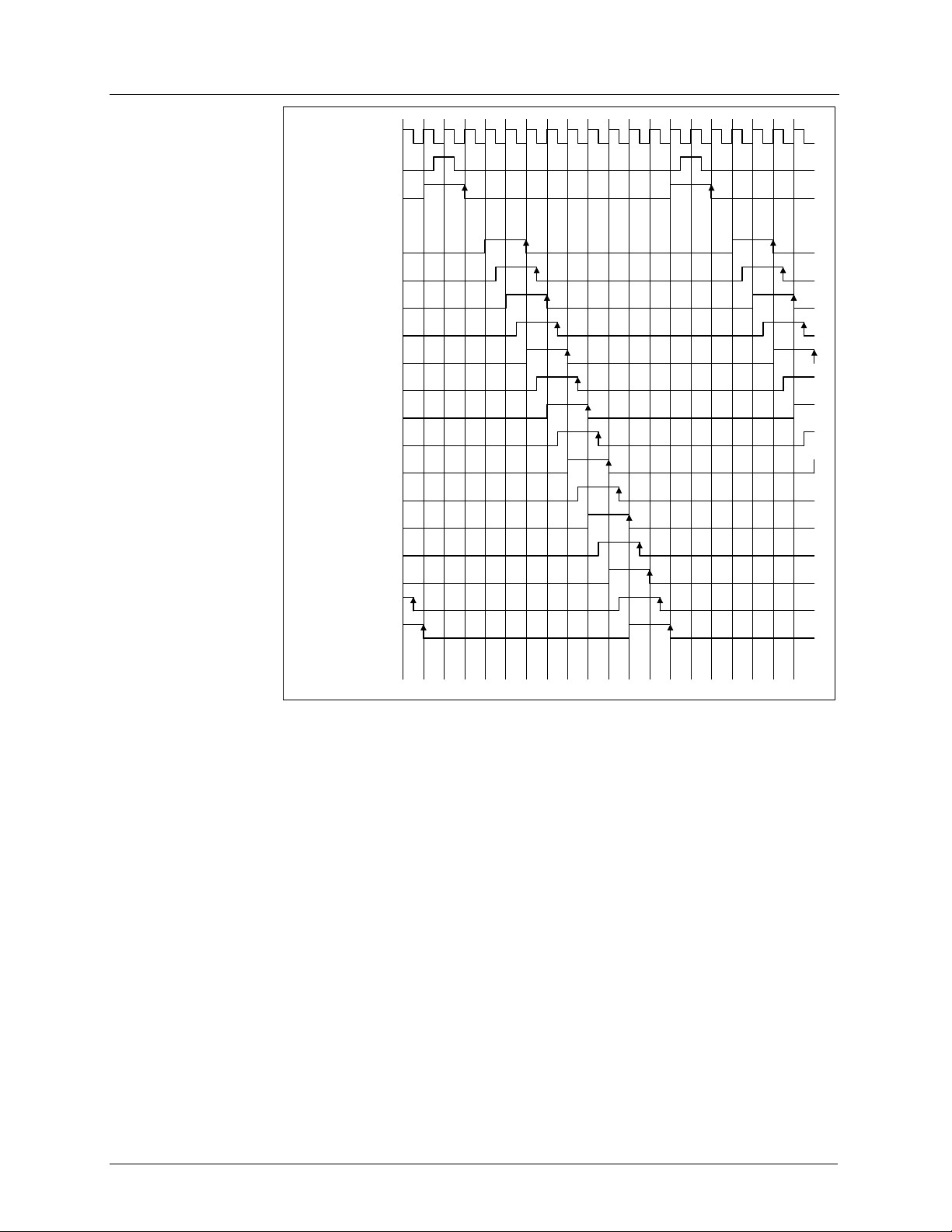
RESET SAMPLE/CLAMP POSITIONS
In CDS modes, cont rol bit s RE SREF [3: 0] c ontrol t he pos iti on of the reset sam pl ing point, R
clamp pulse point, CL, if reset level clamping is selected. In non-CDS modes, control bits
RESREF[3:0] control the position of CL only, if reset level clamping is selected. These diagrams
show the positions to which the sam pling or clamping pulse can be adjust ed for each mode. Care
must be taken to adjus t the R
point will be taken at the most appropriate moment during the reset portion of the input signal.
WOLFSON MICROELECTRONICS LTD
, and the
S
position to one that will ensure that the reset sample and/or clamp
S
PD Rev 4.0 April 1999
24
Page 25
WM8148
THREE-CHANNEL (8-PHASE) – MODES 0 AND 1
Production Data
CCD
Outputs
Time (MCLK)
Phase
MCLK
VSMP
V
S
RS /CL (RESREF=4)
O/P (DEL=00)
O/P (DEL=01)
O/P (DEL=10)
O/P (DEL=11)
4-45-36-27-10011223344556677081
VideoReset VideoReset
Figure 26 Modes 0 and 1 Input Signal Sampling
CCD
Outputs
Time (MCLK)
Phase
MCLK
VSMP
RS /CL (RESREF=4)
O/P (DEL=00)
O/P (DEL=01)
O/P (DEL=10)
O/P (DEL=11)
3194205216227230241252263274285296307310
V
S
RG B
RGB
Reset VideoReset Video
RG B
RG B
9
32
1332
2
Figure 27 Modes 0 and 1 Output Data Timing
WOLFSON MICROELECTRONICS LTD
PD Rev 4.0 April 1999
25
Page 26
WM8148
Production Data
CL (RESREF=0)
✳
✳
CL (RESREF=1)
(RESREF=2)
R
/CL
S
R
/CL
(RESREF=3)
S
/CL
R
(RESREF=4)
S
R
/CL
(RESREF=5)
S
R
/CL
(RESREF=6)
S
/CL
R
(RESREF=7)
S
R
/CL
(RESREF=8)
S
R
/CL
(RESREF=9)
S
RS/CL
(RESREF=10)
6701234567 4567
Phase
0123 01
MCLK
VSMP
V
S
Invalid RESREF positions in CDS Mode (Mode 0)
✳
Figure 28 Modes 0 and 1 Reset Sample/Clamp Positions
WOLFSON MICROELECTRONICS LTD
PD Rev 4.0 April 1999
26
Page 27
WM8148
ONE-CHANNEL CDS – MODE 2
Production Data
CCD
Outputs
Time (MCLK)
Phase
MCLK
VSMP
RS (RESREF=2)
O/P (DEL=00)
O/P (DEL=01)
O/P (DEL=10)
O/P (DEL=11)
2-43-34-25-10011223344550617283
V
S
Figure 29 Mode 2 Input Signal Sampling
CCD
Outputs
Time (MCLK)
Phase
MCLK
VSMP
V
S
RS (RESREF=2)
O/P (DEL=00)
O/P (DEL=01)
O/P (DEL=10)
O/P (DEL=11)
1492503514525530541552563574585590601612
RGB
RGB
Reset VideoReset Video
RGB
Reset
9
ResetReset VideoReset Video
62
RGB
Figure 30 Mode 2 Output Data Timing
RS /CL (RESREF=2)
RS /CL (RESREF=3)
R
/CL (RESREF=4)
S
RS /CL (RESREF=5)
R
/CL (RESREF=6)
S
Figure 31 Mode 2 Reset Sample/Clamp Positions
WOLFSON MICROELECTRONICS LTD
4501234501 0123
Phase
2345 45
MCLK
VSMP
V
S
PD Rev 4.0 April 1999
27
Page 28
WM8148
ONE-CHANNEL NON-CDS – MODE 3
Video Video Video
CCD
Output
Production Data
Time (MCLK)
CL (RESREF=0)
O/P (DEL=00)
O/P (DEL=01)
O/P (DEL=10)
O/P (DEL=11)
-41-32-23-100
0
Phase
MCLK
VSMP
V
S
Figure 32 Mode 3 Input Signal Sampling
CCD
Outputs
Time (MCLK)
Phase
MCLK
VSMP
V
S
CL (RESREF=0)
O/P (DEL=00)
O/P (DEL=01)
O/P (DEL=10)
O/P (DEL=11)
2343350361372383390401412423430441
Video
RGB
RGB
1
2
3
4
1
2
3
5
0
1
7
263
VideoVideo
45
RGB
RGB
Figure 33 Mode 3 Output Data Timing
CL (RESREF=0)
CL (RESREF=1)
CL (RESREF=2)
Figure 34 Mode 3 Reset Sample/Clamp Positions
WOLFSON MICROELECTRONICS LTD
2301230123 0123
0123 01
MCLK
VSMP
V
S
PD Rev 4.0 April 1999
28
Page 29
WM8148
TWO-CHANNEL (6-PHASE) – MODES 4 AND 5
Production Data
CCD
Outputs
Time (MCLK)
Phase
MCLK
VSMP
RS /CL (RESREF=2)
O/P (DEL=00)
O/P (DEL=01)
O/P (DEL=10)
O/P (DEL=11)
2-43-34-25-10011223344550617283
V
S
Figure 35 Modes 4 and 5 Input Signal Sampling
CCD
Outputs
Time (MCLK)
Phase
MCLK
VSMP
V
S
RS /CL (RESREF=2)
O/P (DEL=00)
O/P (DEL=01)
O/P (DEL=10)
O/P (DEL=11)
1192203214225230241252263274285290301312
RG
RG
Reset VideoReset Video
Reset VideoReset Video
RG
RG
Reset
9
32
Figure 36 Modes 4 and 5 Output Data Timing
CL (RESREF=0)
✳
CL (RESREF=1)
✳
/CL (RESREF=2)
R
S
/CL (RESREF=3)
R
S
/CL (RESREF=4)
R
S
RS /CL (RESREF=5)
RS /CL (RESREF=6)
Invalid RESREF positions in CDS mode (Mode 4)
✳
Figure 37 Modes 4 and 5 Reset Sample/Clamp Positions
WOLFSON MICROELECTRONICS LTD
4501234501 0123
2345 45
MCLK
VSMP
V
S
PD Rev 4.0 April 1999
29
Page 30
WM8148
THREE CHANNEL (12-PHASE) – MODES 8 AND 9
Reset Video Reset
CCD
Outputs
Production Data
-1
Time (MCLK)
Phase
MCLK
VSMP
V
S
RS /CL (RESREF=6)
O/P (DEL=00)
O/P (DEL=01)
O/P (DEL=10)
O/P (DEL=11)
6-67-58-49-310-211
001
1
Figure 38 Modes 8 and 9 Input Signal Sampling
CCD
Outputs
Time (MCLK)
Phase
MCLK
VSMP
V
S
RS /CL (RESREF=6)
O/P (DEL=00
O/P (DEL=01)
O/P (DEL=10)
O/P (DEL=11)
933103411350361372383394
RGB
40
43
5416427
RGB
5
4
22334
84494511471493515
10460482504
RGB
7
9
10
667
8
9
10
8
53
6547
55
52
5
RGB
11110121
856957105811
13
59
Figure 39 Modes 8 and 9 Output Data Timing
WOLFSON MICROELECTRONICS LTD
PD Rev 4.0 April 1999
30
Page 31
WM8148
Production Data
MCLK
VSMP
V
S
CL (RESREF=0)
✳
CL (RESREF=1)
✳
/CL (RESREF=2)
R
S
R
/CL (RESREF=3)
S
/CL (RESREF=4)
R
S
R
/CL (RESREF=5)
S
R
/CL (RESREF=6)
S
/CL (RESREF=7)
R
S
R
/CL (RESREF=8)
S
/CL (RESREF=9)
R
S
R
/CL (RESREF=10)
S
RS /CL (RESREF=11)
101101234567 0123
8 9 10 11 4 5
RS /CL (RESREF=12)
RS /CL (RESREF=13)
RS /CL (RESREF=14)
Invalid RESREF positions in CDS mode (Mode 8)
✳
Figure 40 Modes 8 and 9 Reset Sample/Clamp Positions
WOLFSON MICROELECTRONICS LTD
PD Rev 4.0 April 1999
31
Page 32
WM8148
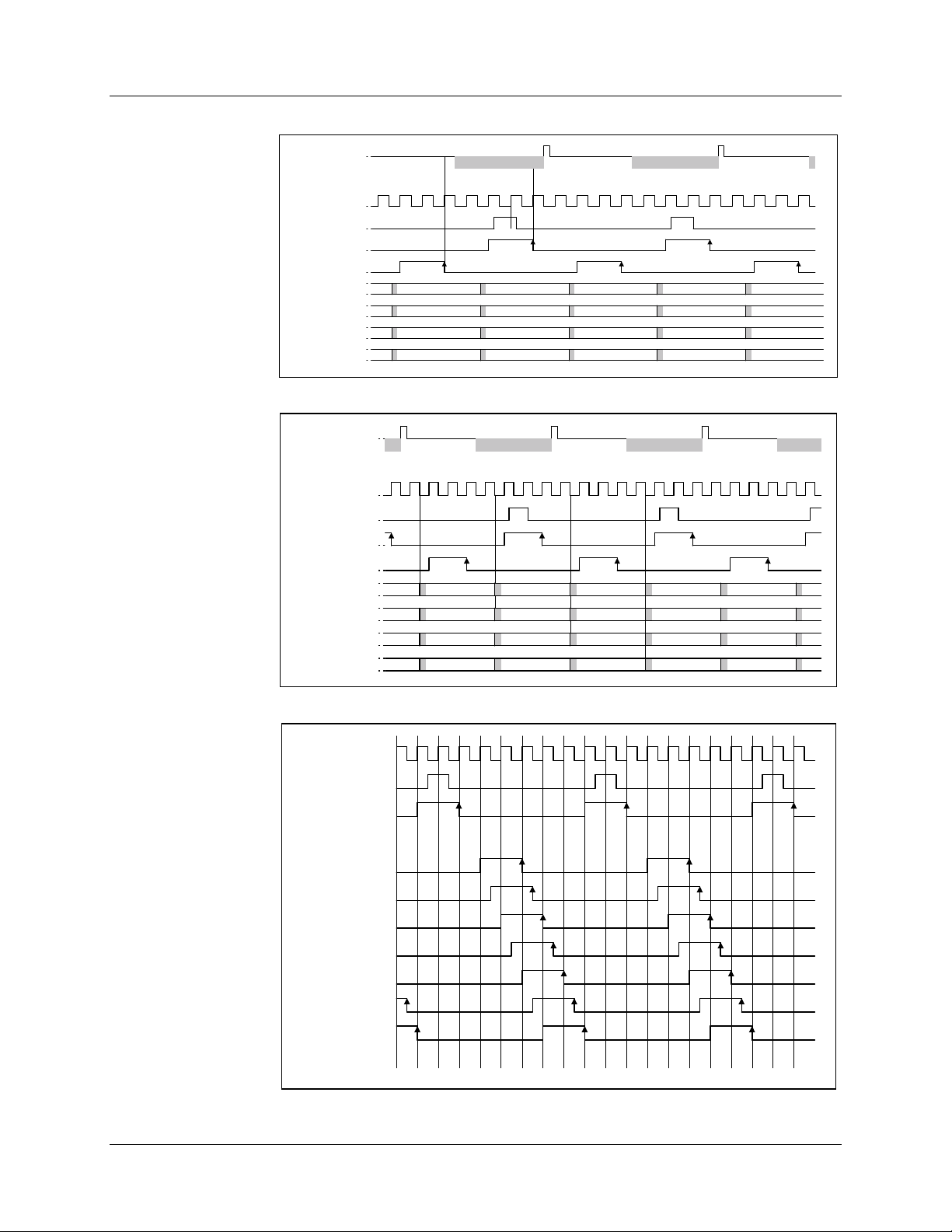
TWO-CHANNEL (8-PHASE) – MODES 12 AND 13
Production Data
CCD
Outputs
Time (MCLK)
Phase
MCLK
VSMP
V
S
RS /CL (RESREF=2)
O/P (DEL=00)
O/P (DEL=01)
O/P (DEL=10)
O/P (DEL=11)
2-63-54-45-36-27
-1
1
22334
001
Figure 41 Modes 12 and 13 Input Signal Sampling
CCD
Outputs
Time (MCLK)
Phase
MCLK
VSMP
V
S
RS /CL (RESREF=2)
O/P (DEL=00
O/P (DEL=01)
O/P (DEL=10)
O/P (DEL=11)
Reset Video Reset Video Reset Video
1332343354365376387390
RG
40
1412423
RG
5
4
45747149351553
43
4445
RG
7
8
667
5
46048250452
6
0
RG
ResetReset VideoVideoReset
9
10
1
2
3114125
6547
13
55
Figure 42 Modes 12 and 13 Output Data Timing
6701234567 4567
MCLK
VSMP
V
S
✳
CL (RESREF=0)
RS/CL (RESREF=1)
/CL (RESREF=2)
R
S
/CL (RESREF=3)
R
S
R
/CL (RESREF=4)
S
RS /CL (RESREF=5)
RS /CL (RESREF=6)
Invalid RESREF positions in CDS mode (Mode 12)
✳
0123 01
Figure 43 Modes 12 and 13 Reset Sample/Clamp Positions
WOLFSON MICROELECTRONICS LTD
PD Rev 4.0 April 1999
32
Page 33

WM8148
DEVICE CONFIGURATION
The following section details the Control Register Map, the contents of which determines the
operation of the WM8148, and the Cont rol Bit tabl e, which describes the possible s ettings of each of
the bits in the Control Regis ter Map.
INTERNAL REGISTER DEFINITION
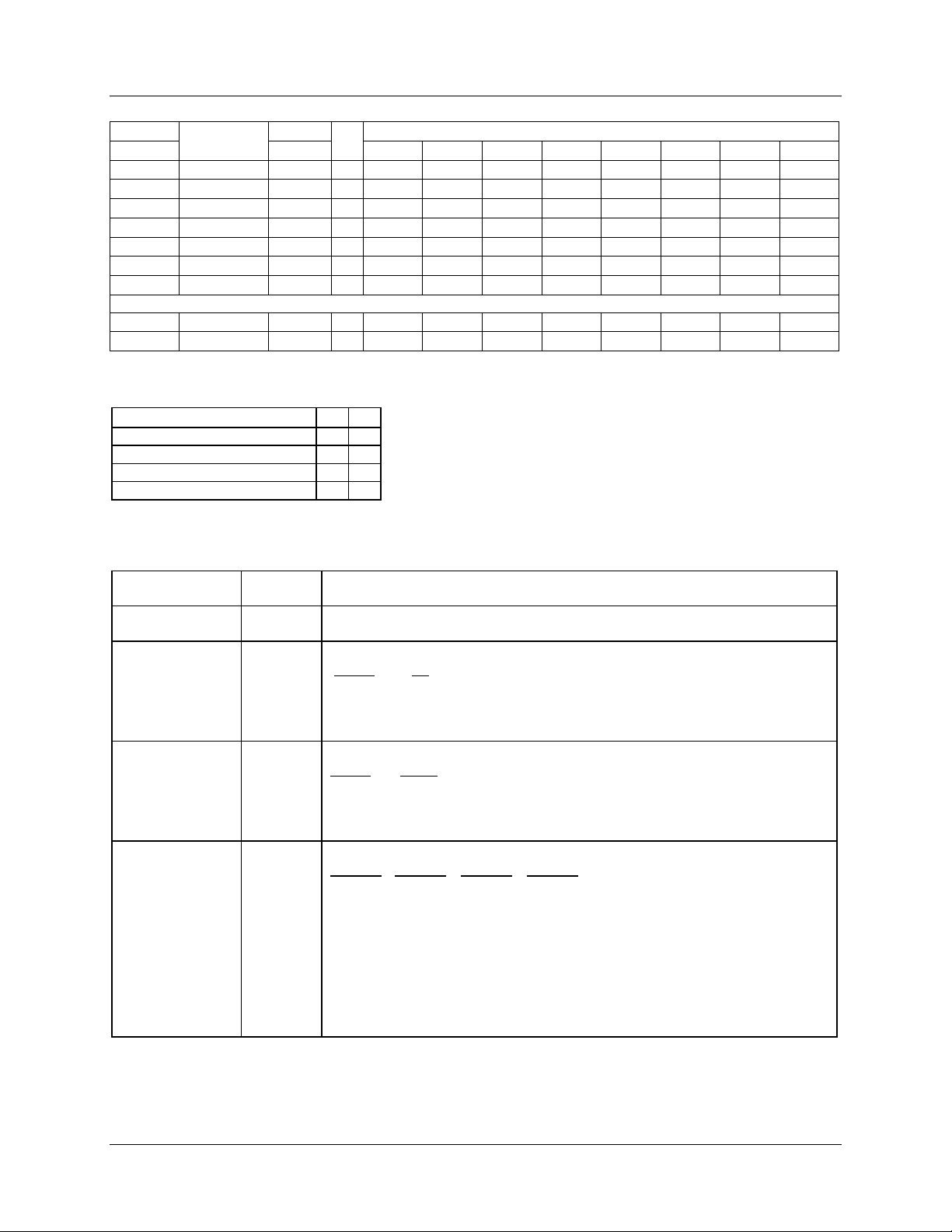
Table 6 details the internal regis ter contents.
SET-UP REGISTER 1
• Selects global power on/off or select i ve enable.
• Selects the function of t he SDO pin.
• Control s i nput sampling mode the device is operating in.
SET-UP REGISTER 2
• Enables individual sections of the device such as sampl e and hol d bl ocks or PGA.
SET-UP REGISTER 3
• Set s the clamp and reset sample position in CDS m odes .
• Set s the clamp position i n non-CDS modes.
• Enables the internal clocks to be free running without VSMP.
• All ows t he vi deo and reset sample pulse widths t o be reduc ed by hal f an MCLK period.
• Selects the channel that the s ample is taken from i n One-Channel (or l i ne by l i ne) modes.
SOFTWARE RESET
• Writing to this regi s ter causes the device to reset. Three different reset types are avai l abl e.
See Control Bit Descript i on Tabl e for details.
SET-UP REGISTER 4
• Al l ows t he l atency through the device to be adjus ted by ADC clock periods and by half -MCLK
periods.
• Enables VSMP as input or output.
• All ows t he external s etting of RLC bias reference voltage.
• Control s paral l el /multiplexed output form at .
• Defi nes the polarity of the output data.
COARSE OFFSETS
• Control s the non-CDS reference voltage level or res e t clamp level.
• All ows external ref erenc e to be used as reset clamp l evel .
• Adjusts the d.c. level of t he PGA outputs to align with the ADC i nput range to suit different input
video signal polarities.
REVISION NUMBER
• All ows t he user to check which revision of t he devi c e i s being used.
DAC VALUES
• Programmes the amount of offset applied to the input of each PGA. Table 7 describes t he
sub-address bits for each channel.
PGA GAINS
• Programmes the gain of each PG A . Table 7 describes the sub-address bi ts for each channel.
Production Data
WOLFSON MICROELECTRONICS LTD
PD Rev 4.0 April 1999
33
Page 34
WM8148
Production Data
ADDRESS DEFAULT BIT
<A5:A 0>
000001
000010
000011
000100
000101
000110
000111
1000
1010
Note:
DESCRIPTION
Setup Register 1
Setup Register 2
Setup Register 3
Software Reset
Setup Register 4
Coarse Offsets
Revision Number
DAC Values
XY
PGA Gains
XY
(HEX)
RW
80 RW
00 RW
06 RW
00 W
00 RW
1B RW
43 R
80 RW
00 RW
B7 B6 B5 B4 B3 B2 B1 B0
MODE[3] MODE[2] MODE[1] MODE[0] SDO[1] SDO[0] SELEN EN
SENBL[7] SENBL[6] SENBL[5] SENBL[4] SENBL[3] SENBL[2] SENBL[1] SENBL[0]
CHAN[1] CHAN[0] SMALL FREE RESREF[3] RESREF[2] RESREF[1 ] RESREF[0]
0 0 0 0 0 0 SRES[1] SRES[0]
INVOP MUXOP 0 VSMPOP FDEL[1] FDEL[0] DEL[1] DEL[ 0]
0 PGAFS[1] PGAFS[0] RLCEXT RLCV[3] RLCV[2] RLCV[1] RLCV[0]
REV[7] REV[6] REV[5] REV[4] REV[3] REV[2] REV[1] REV[0]
DAC[7] DAC[6] DAC[5] DAC[4] DAC[3] DAC[2] DAC[1] DAC[0]
0 0 PGA[5] PGA[4] PGA[3] PGA[2] PGA[1] PGA[0]
Register address 000000 is reserved and s houl d not be written to.
Table 6 Control Register Map
ADDRESS LSB DECODE X Y
Red register 0 0
Green register 0 1
Blue register 1 0
Red, Green, and Blue registers 1 1
Table 7 Red, Green, Blue, Sub-address Bits
CONTROL BIT DESCRIPTION
CONTROL
BIT/WORD
Set-up Register 1 Address
EN b0
SELEN b1
SDO[1:0]
b3, b2
MODE[3:0]
b7, b6, b5, b4
DEFAULT DESCRIPTION
000001
0
0
Global power on/off or selective enable.
SELEN EN
0 0 Complete power down (default).
0 1 Complete power on.
1 X Individual bl ock power on/off (X denotes either 1 or 0)
00
Multiplexes SDO output pin.
SDO[1] SDO[0
0 0 Regi ster readback when requested, Hi-Z otherwise
0 1 TVIOL flag (RESREF incons i stent with MODE).
1 0 ADC over-range flag.
1 1 VSMP synchronous output.
1000
Device mode control bits.
MODE[3] MODE[2]
0 0 0 0 Three-channel (8-phase) CDS
0 0 0 1 Three-channel (8-phase) non-CDS
0 0 1 0 One-channel CDS
0 0 1 1 One-channel non-CDS
0 1 0 0 Two-channel (6-phase) CDS
0 1 0 1 Two-channel (6-phase) non-CDS
1 0 0 0 Three-channel (12-Phase) CDS
1 0 0 1 Three-channel (12-Phase) non-CDS
1 1 0 0 Two-channel (8-Phase) CDS
1 1 0 1 Two-channel (8-Phase) non-CDS
see SENBL[7:0] regis t er description for details.
]
MODE[1] MODE[0]
WOLFSON MICROELECTRONICS LTD
PD Rev 4.0 April 1999
34
Page 35
WM8148
Production Data
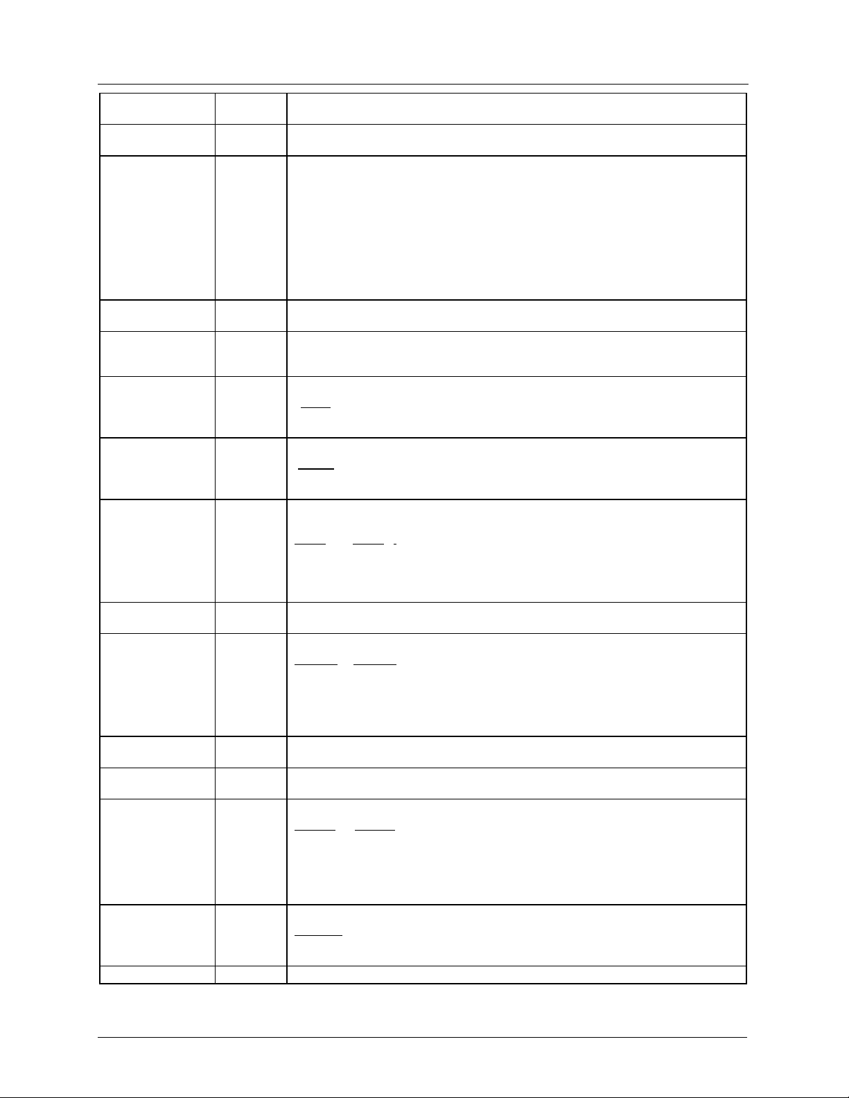
CONTROL
BIT/WORD
Set-up Register 2 Address
SENBL[7:0]
b7…..b0
Set-up Register 3 Address
RESREF[3:0]
b3, b2, b1, b0
FREE
b4
SMALL
b5
CHAN[1:0]
b7, b6
Software Reset Address
SRES[1:0]
b1, b0
Setup Register 4 Address
DEL[1:0]
b1, b0
FDEL[1:0]
b3, b2
VSMPOP
b4
b5 0
DEFAULT DESCRIPTION
000010
0000
0000
000011
0110
0
0
00
000100
00
000101
00
00
0
Selective power enable register, act i vated when SELEN = 1 (Set-up Register 1).
Each bit activates respective cell when 1, de-activates when 0.
SENBL[0] Bandgap/Bias
SENBL[1] VRT, VRB buffers
SENBL[2] VRX buffer
SENBL[3] RLC DAC (allows VRLC t o be externall y dri ven)
SENBL[4] Red S/H, PGA
SENBL[5] Green S/H, P G A
SENBL[6] Blue S/H, PGA
SENBL[7] ADC
Selects the posit i on of ei ther the reset sample and the clamp points in CDS modes,
or the position of just the clamp pulse in non-CDS modes. See Mode Descriptions f or
further details.
Enables internal clocks to be free running, without VSMP pulse input.
FREE
0 Requires continuous VSMP pulse input every N periods of MCLK
1 Free running
Reduces video and reset sampl e pul se widths by half an MCLK period.
SMALL
0 Default pulse widths
1 Reduces pulse widths
Selects the input c hannel i n One-channel (line by line) modes.
No effect when not in One-channel mode.
CHAN[1] CHAN
0 0 Red channel
0 1 Green channel
1 0 Blue channel
11 Reserved
Writing to t hi s register causes a software reset. There a three types of reset availabl e:
SRES[1] SRES[0]
0 0 Same action as NRES E T pi n
0 1 Resets all registers to default including RLCEXT.
1 X Resets PGA and DAC only (X denotes either 1 or 0)
Adjusts the lat ency through the device in ADC cloc k periods.
See Detailed Mode Timing Diagram s for details.
Adjusts the latenc y t hrough the device in half-MCLK increment s.
FDEL[1] FDEL[0]
0 0 Default position
0 1 Earlier by MCLK/2
1 0 Later by MCLK/2 Invalid in modes 0, 1, 4 and 5
1 1 Later by MCLK/2 Invalid in modes 0, 1, 4 and 5
In these invalid modes, output data is held const ant , TVIOL is not flagged.
Enables output of internall y generat ed MCLK/ N sync pulse (only if FREE also set).
VSMPOP
0 Requires external VSMP
1 VSMP pin becomes sync output
Reserved for Wolfson use only, must be programmed to 0.
[0]
(Except EN, SELEN and SENBL[7:0], which are
not changed)
WOLFSON MICROELECTRONICS LTD
PD Rev 4.0 April 1999
35
Page 36
WM8148
Production Data
CONTROL
BIT/WORD
MUXOP
b6
INVOP
b7
Coarse Offsets Address
RLCV[3:0]
b3, b2, b1, b0
RLCEXT
b4
PGAFS[1:0]
b6, b5
Revision Number Address
REV[7:0]
b7, …..b0
DAC Values Address
DAC[7:0]
b7, …..b0
PGA Gains Address
PGA[5:0]
b5, ….. b0
Table 8 Control Register Bit Descriptions
DEFAULT DESCRIPTION
0
0
000110
1011
1
00
000111
43
1000xy
1000
0000
1010xy
000000
Changes the data output form at from 12-bit parallel to 2 x 8 bit m ul t i pl exed.
MUXOP
Digitally inverts the pol ari ty of output data.
INVOP
Controls RLC DAC driving VRLC pin, to def i ne single-ended signal-reference voltage
or reset-level clamp volt age. F(hex) is VDD, 0(hex) is 0V, B(hex) (default) is 11/15 ∗
AVDD (= 3.67V typicall y).
Powers down the RLC DAC, tri-stating its output, allowing VRLC to be externally driven.
RLCEXT
Configures the ADC input to ac c ept the following video signal types:
PGAFS[1] PGAFS[0]
Read-only register, allows the user to determine the revision l evel of the device.
ASCII 7-bit code, e. g. 43(hex) = C
The offset-setting dat a for the Red, Green and Blue offset DA Cs. 00(hex) gives
-200mV offset referred to signal input, FF(hex) gives +200mV, 80(hex) (default) gives
approximately zero offset.
The gain setting data for the Red, Green, and Blue programmable gain ampl i fiers.
00(hex) gives min gain, 3F(hex) gives max gain.
0 12-bit wide parallel data
1 8-bit wide multiplexed data
0 Negative-going video gives negative-going output data
1 Negative-going video gives positive-going output data
0 RLC DAC drives VRLC pin
1 RLC DAC Hi-Z
0 0 Bipolar video
0 1 Bipolar video
1 0 Negative-going video
1 1 Positive-going video
WOLFSON MICROELECTRONICS LTD
PD Rev 4.0 April 1999
36
Page 37
WM8148
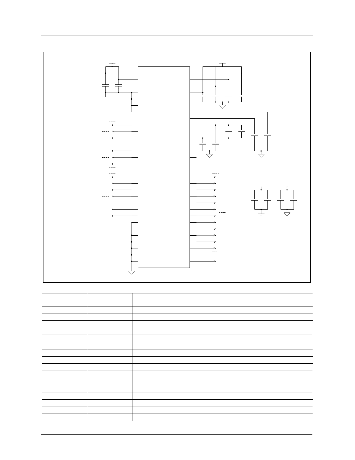
RECOMMENDED EXTERNAL COMPONENTS
DVDD AVDD
C2C1
DGND
Video
Inputs
Timing
Signals
Interface
Controls
C1-12 should be fitted as close toNOTES:
1.
WM8148 as possible.
AGND and DGND should be connected
2.
as close to WM8148 as possible.
1
DVDD1
13
DVDD2
8
DGND1
24
DGND2
4
DGND3
26
DGND4
36
RINP
37
GINP
39
BINP
5
MCLK
7
VSMP
2
RLC
46
SCK/RNW
47
SEN/STB
45
SDI/DNA
48
PNS
43
OEB
42
NRESET
34
OVRD
35
AGND1
40
AGND2
30
AGND3
25
AGND4
6
AGND5
WM8148
AVDD1
AVDD2
AVDD3
AVDD4
VRLC
VRX
VRT
VRB
NC
NC
NC
OP11
OP10
OP9
OP8
OP7
OP6
OP5
OP4
OP3
OP2
OP1
OP0
SDO
41
28
27
3
C3 C4 C5 C6
33
32
31
29
C11 C12
38
23
22
21
20
19
18
17
16
15
14
12
11
10
9
44
AGND
C7 C8
Output
Data
Bus
Serial
Output
Production Data
C9 C10
AGNDAGND
DVDD
++++
DGND AGND
AVDD
C14C13
C16C15
AGND
Figure 44 External Components Diagram
COMPONENT
REFERENCE
SUGGESTED
VALUE
C1 10nF
C2 10nF
C3 10nF
C4 10nF
C5 10nF
C6 10nF
C7 10nF
C8 1 µF
C9 100nF
C10 100nF
C11 100nF
C12 100nF
C13 1µF
C14 1µF
C15 1µF
C16 1µF
Table 9 External Components Descriptions
WOLFSON MICROELECTRONICS LTD
DESCRIPTION
De-coupling for DVDD1.
De-coupling for DVDD2.
De-coupling for AVDD4.
De-coupling for AVDD3.
De-coupling for AVDD2.
De-coupling for AVDD1.
High frequency de-coupling between VRT and VRB.
Low frequency de-coupling between VRT and VRB (non-polarised).
De-coupling for VRX.
De-coupling for VRLC.
De-coupling for VRB.
De-coupling for VRT.
Reservoir capacitor for DV DD.
Reservoir capacitor for DV DD.
Reservoir capacitor for A V DD.
Reservoir capacitor for A V DD.
PD Rev 4.0 April 1999
37
Page 38

WM8148
APPLICATIONS RECOMMENDATIONS
INTRODUCTION
The WM8148 is a mixed signal device, therefore caref ul PCB layout is requi red. The f ollowing sec ti on
contains PCB layout guideli nes, which are recom mended for optimal perf orm ance f rom t he WM8148,
and some typical applic ations circuits.
PCB LAYOUT
1) Use separate analogue and digi tal power and ground planes. The analogue and digital ground
planes should be connected as c l ose as possible to, or underneath, the WM8148.
2) Place all supply decoupling capacit ors as close as pos sible to t heir respective s upply pins and
provide a low impedance path from t he capacitors to the appropriate ground.
3) Avoid noise on AGND (in particular on pins 30, 35 and 40).
4) Avoid noise on reference pins VRT, VRB and VRX. Place the decoupl ing capaci tors as close as
possible to these pins and provide a low impedance path from the capacitors to analogue
ground.
5) Input signals should be screened from each other and from other sources of noise to avoid
cross talk and interf erence.
6) Minimise load capacitance on digital outputs. Capacitive loads of greater than 20pF will degrade
performance. Use buff ers if necessary and keep tracks short.
TYPICAL APPLICATIONS DIAGRAMS
CCDs are available in four basic t ypes t hat are all compatible with the WM8148.
Production Data
• Monochrome single output.
• Monochrome odd-even output.
• Colour 3 out put .
• Colour 6 out put .
Each of these applicat i ons is outlined in this section.
The output from a CCD sensor usually has a high impedance and must therefore be buffered
as close to the sensor as poss ible. The sensor manufacturers’ datasheets specify the buff er circuit
to use.
Initially, the designer m ust decide if CDS and Reset Level Clamping is to be used. The WM8148
supports both of these functions and Wolfson recommend using both CDS and pixel-by-pixel
clamping for optimal performance. In this case a low value a.c. coupling capacitor is required
between the sensor and the WM8148. Experiments have shown that a 100pF capacitor is the
optimum value to use, however this may vary for particular applications depending on speed of
operation and PCB layout.
WOLFSON MICROELECTRONICS LTD
PD Rev 4.0 April 1999
38
Page 39
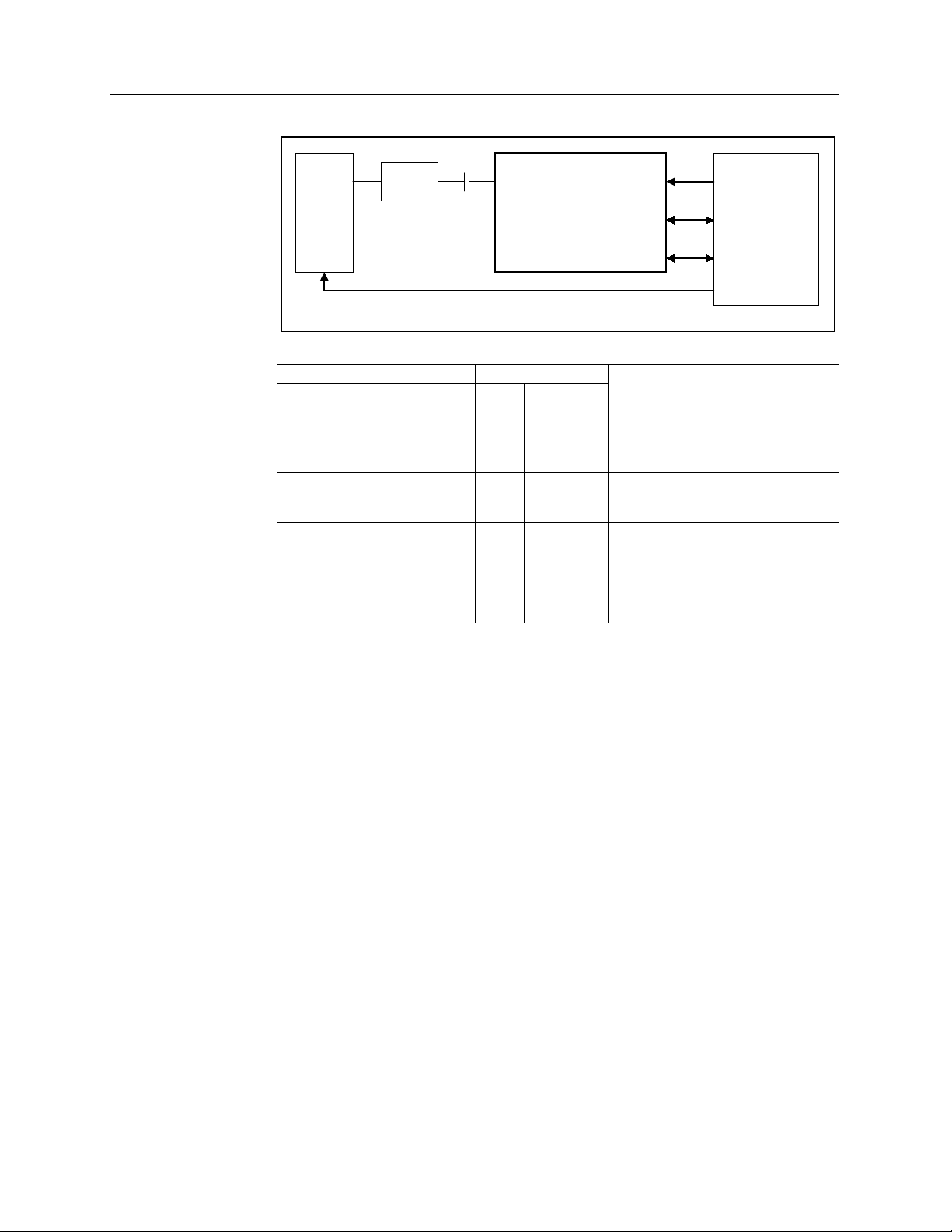
WM8148
Production Data
MONOCHROME SINGL E OUTPUT
S
OUT
E
N
S
O
BUFFER
See sensor
datasheet for
details
R
SENSOR TIMING
Maximum Pixel Rate = 6.66Mpixels/second (Mode 2)
C
RINP
WM8148
Including
recommended
external
components
CONTROL I/F
Figure 45 Block Diagram of Monochrome CCD Application
REGISTER SETTING
DESCRIPTION ADDRESS HEX BINARY
Set-up register 1 000001 22 0010 0010
Set-up register 2 000010 9F 1001 1111
Set-up register 3 000011 02 0000 0010
Set-up register 4 000101 80 1000 0000
Coarse offsets 000110 4B 0100 1011
Table 10 Typical Control Register Settings for Figure 45
(CDS, Negative-Going CCD Video Signal, M CL K/VSMP = 6)
CLOCKSV
DATA
SYSTEM
ASIC
NOTE
MODE: Mode 2: single-channel CDS
SELEN: selective power enable
SENBL: green/blue PGAs
powered off
CHAN: red channel select ed
RESREF: reset sample half-way
between video samples
INVOP: invert digital output
(White = 4095)
PGAFS: ADC set up for negative
polarity video
RLCEXT, RLCV: internal VRLC
voltage, set to 3.7V
WOLFSON MICROELECTRONICS LTD
PD Rev 4.0 April 1999
39
Page 40
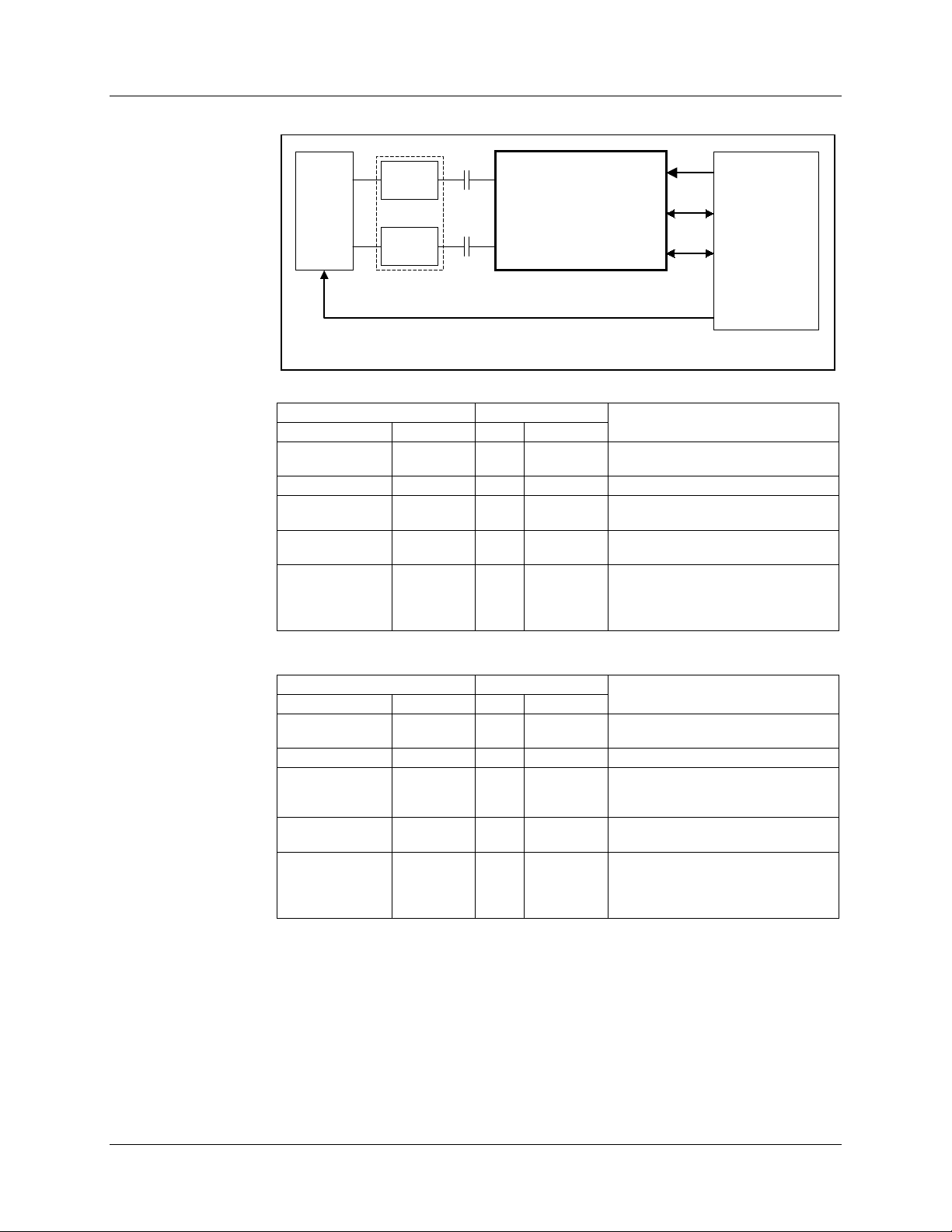
WM8148
MONOCHROME ODD-EVE N OUTP UT
C
S
O
E
BUFFER
N
S
O
E
R
Maximum Pixel Rate = 10.66Mpixels/second (Mode 4)
Maximum Pixel Rate = 12Mpixels/second (Mode 12)
BUFFER
See sensor
datasheet for
details.
O
RINP
WM8148
Including
recommended
C
E
GINP
external
components
SENSOR TIMING
CLOCKS
DATA
CONTROL I/F
Figure 46 Block Diagram of Monochrome CCD (Odd-Even Outputs) Application
Production Data
SYSTEM
ASIC
REGISTER SETTING
DESCRIPTION ADDRESS HEX BINARY
Set-up register 1 000001 42 0100 0010
Set-up register 2 000010 BF 1011 1111
Set-up register 3 000011 02 0000 0010
Set-up register 4 000101 80 1000 0000
Coarse offsets 000110 4B 0100 1011
Table 11 Typical Control Register Settings for Figure 46
(CDS, Negative-Going CCD Video Signal, M CL K/VSMP = 6)
REGISTER SETTING
DESCRIPTION ADDRESS HEX BINARY
Set-up register 1 000001 C2 1100 0010
Set-up register 2 000010 BF 1011 1111
Set-up register 3 000011 02 0000 0010
Set-up register 4 000101 80 1000 0000
Coarse offsets 000110 4B 0100 1011
Table 12 Typical Control Register Settings for Figure 46
(CDS, Negative-Going CCD Video Signal, M CL K/VSMP = 8)
NOTE
MODE: Mode 4: Two-channel CDS
SELEN: selective power enable
SENBL: blue PGAs powered off
RESREF: reset sample half-way
between video samples
INVOP: invert digital output
(White = 4095)
PGAFS: ADC set up for negative
polarity video
RLCEXT, RLCV: internal VRLC
voltage, set to 3.7V
NOTE
MODE: Mode 12: Two-channel CDS
SELEN: selective power enable
SENBL: blue PGAs powered off
CHAN: red channel select ed
RESREF: reset sample half-way
between video samples
INVOP: invert digital output
(White = 4095)
PGAFS: ADC set up for negative
polarity video
RLCEXT, RLCV: internal VRLC
voltage, set to 3.7V
WOLFSON MICROELECTRONICS LTD
PD Rev 4.0 April 1999
40
Page 41
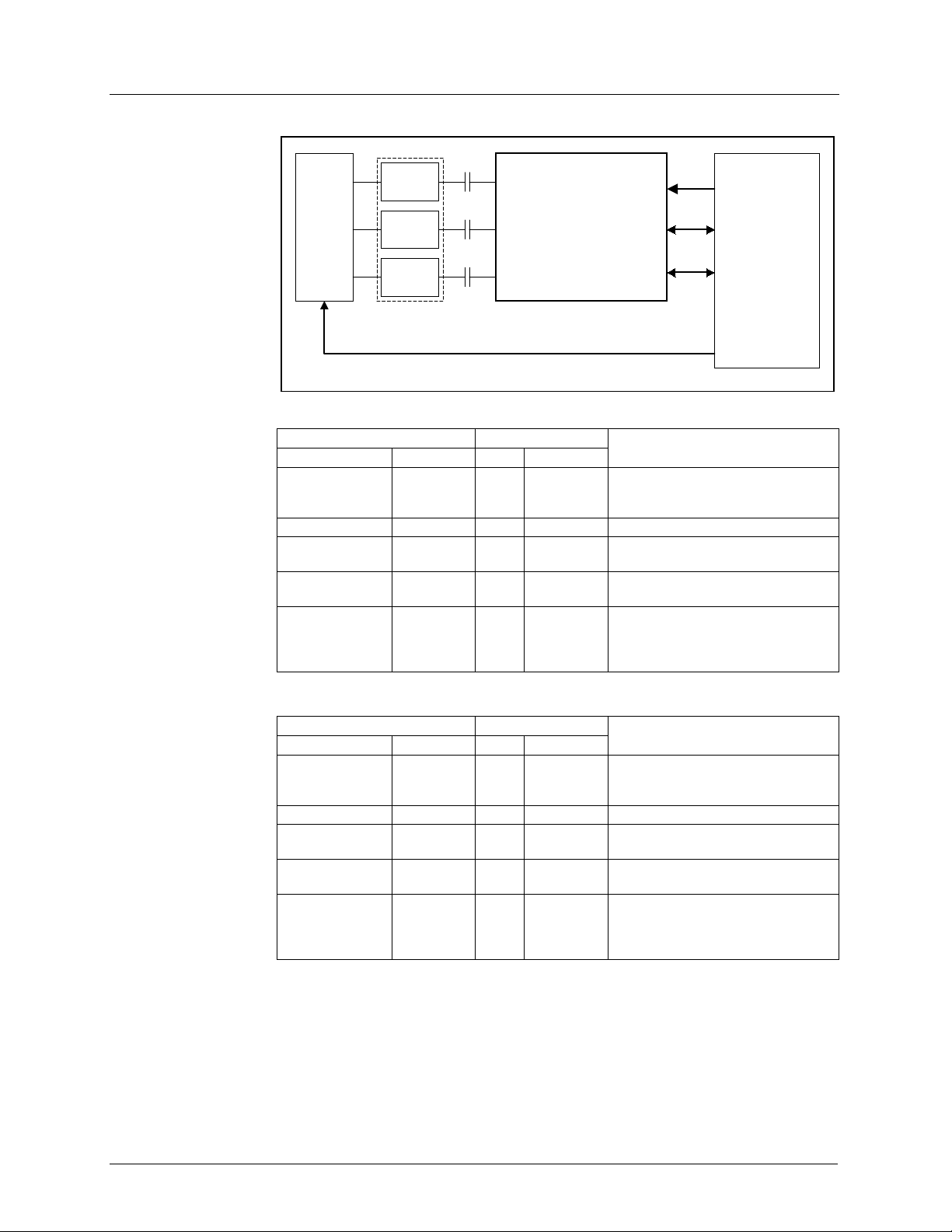
WM8148
COLOUR 3 OUTPUT
C
R
R
S
BUFFER
E
N
G
S
BUFFER
O
R
B
Maximum Pixel Rate = 4Mpixels/second (Modes 0 and 8)
BUFFER
See sensor
datasheet for
details.
RINP
C
G
C
B
WM8148
GINP
recommended
BINP
SENSOR TIMING
Including
external
components
Figure 47 Block Diagram o f Co lour CCD Application
CLOCKS
DATA
CONTROL I/F
Production Data
SYSTEM
ASIC
REGISTER SETTING
DESCRIPTION ADDRESS HEX BINARY
Set-up register 1 000001 01 0000 0001
Set-up register 2 000010 00 0000 0000
Set-up register 3 000011 04 0000 0100
Set-up register 4 000101 80 1000 0000
Coarse offsets 000110 4B 0100 1011
Table 13 Typical Control Register Settings for Figure 47
(CDS, Negative-Going CCD Video Signal, M CL K/VSMP = 8)
REGISTER SETTING
DESCRIPTION ADDRESS HEX BINARY
Set-up register 1 000001 81 1000 0001
Set-up register 2 000010 00 0000 0000
Set-up register 3 000011 06 0000 0110
Set-up register 4 000101 80 1000 0000
Coarse offsets 000110 4B 0100 1011
Table 14 Typical Control Register Settings for Figure 47
(CDS, Negative-Going CCD Video Signal, M CL K/VSMP = 12)
NOTE
MODE: Mode 0: Three-channel CDS
(8-phase)
SELEN, EN: fully enabled
Default (don’t care)
RESREF: reset sample half-way
between video samples
INVOP: invert digital output
(White = 4095)
PGAFS: ADC set up for negative
polarity video
RLCEXT, RLCV: internal VRLC
voltage, set to 3.7V
NOTE
MODE: Mode 8: Three-channel CDS
(12-phase)
SELEN, EN: fully enabled
Default (don’t care)
RESREF: reset sample half-way
between video samples
INVOP: invert digital output
(White = 4095)
PGAFS: ADC set up for negative
polarity video
RLCEXT, RLCV: internal VRLC
voltage, set to 3.7V
WOLFSON MICROELECTRONICS LTD
PD Rev 4.0 April 1999
41
Page 42
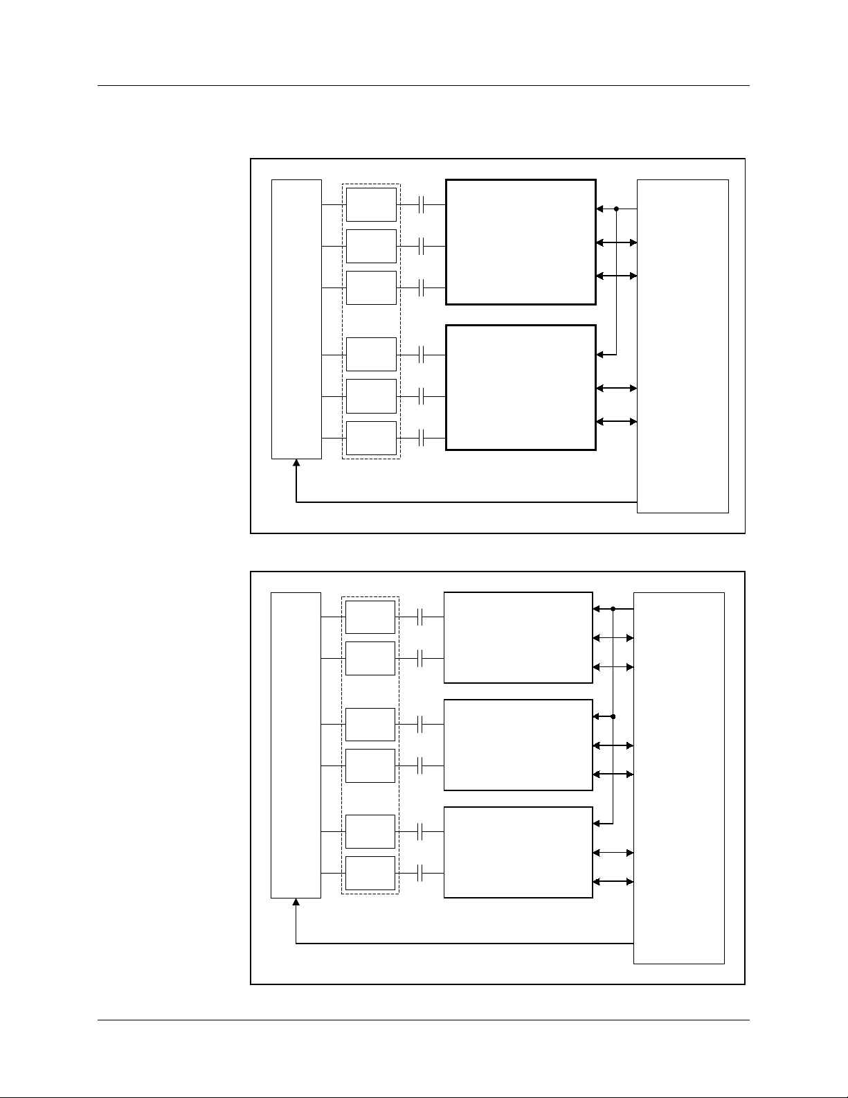
WM8148
Production Data
COLOUR 6 OUTPUT
For applications that require higher pixel rates, multiple W M8148 devic es can be used. The f ollowing
diagrams show typical conf i gurat i ons.
C
RE
R
E
G
S
B
E
BUFFER
BUFFER
E
BUFFER
E
RINP
GINP
BINP
WM8148
Including
recommended
external
components
C
GE
C
BE
CLOCKS
DATA
CONTROL I/F
N
S
O
R
R
O
G
O
B
O
BUFFER
BUFFER
BUFFER
See sensor
datasheet for
details.
C
RO
RINP
C
GO
C
BO
recommended
GINP
BINP
SENSOR TIMING
WM8148
Including
external
components
CLOCKS
DATA
CONTROL I/F
SYSTEM
ASIC
Figure 48 Block Diagram Showing Dual Architecture
C
RE
R
R
O
S
G
E
N
S
G
O
O
BUFFER
E
C
RO
BUFFER
C
GE
BUFFER
E
C
GO
BUFFER
RINP
GINP
RINP
GINP
WM8148
Including
recommended
external
components
WM8148
Including
recommended
external
components
R
C
B
E
B
O
BUFFER
BUFFER
See sensor
datasheet for
details.
BE
C
BO
WM8148
RINP
recommended
GINP
SENSOR TIMING
Including
external
components
CLOCKS
DATA
CONTROL I/F
CLOCKS
DATA
CONTROL I/F
CLOCKS
DATA
CONTROL I/F
SYSTEM
ASIC
Figure 49 Block Diagram Showing Triple Architecture
WOLFSON MICROELECTRONICS LTD
PD Rev 4.0 April 1999
42
Page 43
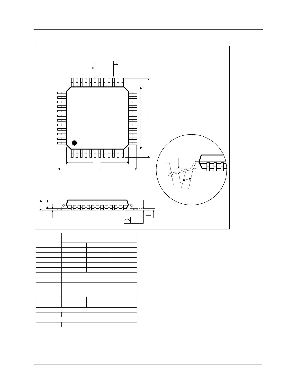
WM8148
(
)
PACKAGE DIMENSIONS
Production Data
FT: 48 PIN TQFP
48
7 x 7 x 1.0 mm
DM004.C
b
D1
D
e
2536
2437
E1 E
13
121
c
Θ
L
A1
A2
A
-C-
SEATING PLANE
C
ccc
Dimensions
Symbols
(Millimeters)
MIN NOM MAX
A
A
1
A
2
b
c
D
D
1
E
E
1
e
L
Θ
----- ----- 1.20
0.05 ----- 0.15
0.95 1.00 1.05
0.17 0.22 0.27
0.09 ----- 0.20
9.00 BSC
7.00 BSC
9.00 BSC
7.00 BSC
0.50 BSC
0.45 0.60 0.75
o
0
3.5
o
7
o
Tolerances of Form and Position
ccc
REF:
NOTES:
A. ALL LINEAR DIMENSIONS ARE IN MILLIMETERS.
B. THIS DRAWING IS SUBJECT TO CHANGE WITHOUT NOTICE.
C. BODY DIMENSIONS DO NOT INCLUDE MOLD FLASH OR PROTRUSION, NOT TO EXCEED 0.25MM.
D. MEETS JEDEC.95 MS-026, VARIATION = ABC. REFER TO THIS SPECIFICATION FOR FURTHER DETAILS.
0.08
JEDEC.95, MS-026
WOLFSON MICROELECTRONICS LTD
PD Rev 4.0 April 1999
43
 Loading...