

Page 1
VN750
TYPE R
DS(on)
I
OUT
V
CC
VN750
VN750S
60 mΩ 6 A 36 V
VN750-B5
■ CMOS COMPATIBLE INPUT
■ ON STATE OPEN LOAD DETECTION
■ OFF STATE OPEN LOAD DETECTION
■ SHORTED LOAD PROTECTION
■ UNDERVOLTAGE AND OVERVOLTAGE
SHUTDOWN
■ PROTECTION AGAINST LOSS OF GROUND
■ VERY LOW STAND-BY CURRENT
■ REVERSE BATTERY PROTECTION (*)
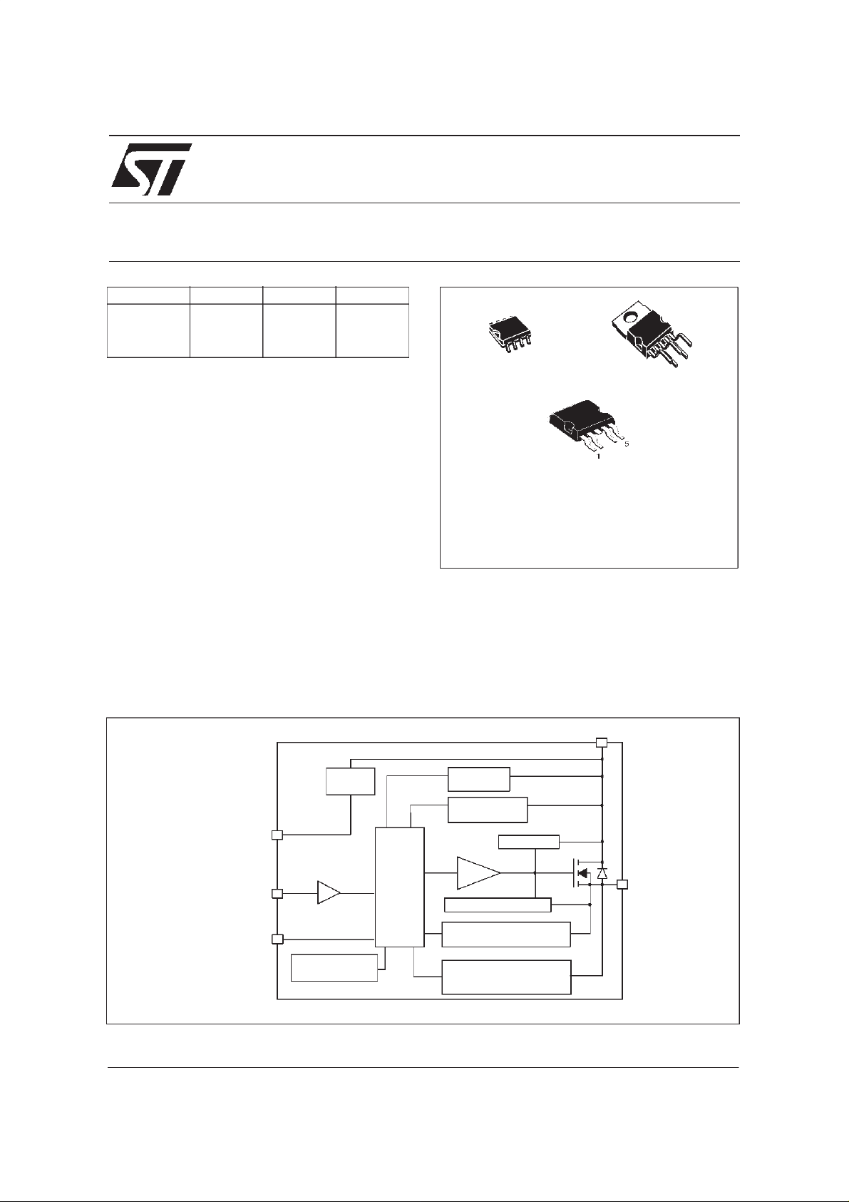
DESCRIPTION
The VN750, VN750S, VN750-B5 are a monolithic
device designed in STMicroelectronics VIPower
Technology, intended for driving any kind of load
with one side connected to ground.
Active V
pin voltage clamp protects the device
CC
against low energy spikes (see ISO7637 transient
compatibility table). Active current limitation
/ VN750S / VN750-B5
HIGH SIDE DRIVER
SO-8
ORDER CODES :
PENTAWATT
SO-8
P2PAK
combined with thermal shutdown and automatic
restart protect the device against overload.
The device detects open load condition both is on
and off state. Output shorted to VCCis detected in
the off state.Device automatically turns off in case
of ground pin disconnection.
PENTAWATT
P2PAK
VN750
VN750S
VN750-B5
BLOCK DIAGRAM
V
CC
V
CC
CLAMP
GND
INPUT
STATUS
(*) See application schematic at page 8
OVERTEMPERATURE
DETECTION
LOGIC
January 2000 1/15
OVERVOLTAGE
DETECTION
UNDERVOLTAGE
DETECTION
Power CLAMP
DRIVER
CURRENT LIMITER
ON STATE OPENLOAD
DETECTION
OFF STATE OPENLOAD
AND OUTPUT SHORTED TO V
DETECTION
OUTPUT
CC
1
Page 2

VN750 / VN750S / VN750-B5
ABSOLUTE MAXIMUM RATING
Symbol Parameter
V
CC
-V
-I
gnd
I
OUT
-I
OUT
I
IN
I
STAT
V
ESD
P
T
T
T
stg
CONNECTION DIAGRAM (TOP VIEW)
DC Supply Voltage 41 V
Reverse DC Supply Voltage - 0.3 V
CC
DC Reverse Ground Pin Current - 200 mA
DC Output Current Internally Limited A
Reverse DC Output Current - 6 A
DC Input Current +/- 10 mA
DC Status Current +/- 10 mA
Electrostatic Discharge (R=1.5KΩ; C=100pF) 2000 V
Power Dissipation TC=25°C 3.1 42 42 W
tot
Junction Operating Temperature Internally Limited °C
j
Case Operating Temperature - 40 to 150 °C
c
Storage Temperature - 55 to 150 °C
Value
SO-8 PENTAWATT P2PAK
Unit
V
CC
OUTPUT
OUTPUT
V
CC
5
8
4
N.C.
STATUS
INPUT
1
GND
SO-8
CURRENT AND VOLTAGE CONVENTIONS
I
IN
INPUT
I
STAT
STATUS
V
IN
V
STAT
V
CC
GND
OUTPUT
I
GND
P2PAK
PENTAWATT
I
OUT
V
OUT
I
CC
OUTPUT
STATUS
V
CC
INPUT
GND
V
CC
5
4
3
2
1
2/15
1
Page 3

THERMAL DATA
Symbol Parameter
R
thj-pins
R
thj-amb
R
thj-case
Thermal Resistance Junction-pins Max 40 - - °C/W
Thermal ResistanceJunction-ambient
Thermal Resistance Junction-case
Max
Max
VN750 / VN750S / VN750-B5
Value
S0-8 PENTAWATT P2PAK
120 60 60 °C/W
-33°C/W
Unit
ELECTRICAL CHARACTERISTICS(8V<V
<36V; -40°C<Tj<150°C unless otherwise specified)
CC
POWER
Symbol Parameter Test Conditions Min Typ Max Unit
V
CC
V
USD
V
USDhyst
V
OV
R
ON
I
I
L(off1)
I
L(off2)
SWITCHING (V
Symbol Parameter TestConditions Min Typ Max Unit
t
d(on)
t
d(off)
dV
OUT
dt
(on)
dV
OUT
dt
(off)
Operating Supply Voltage 5.5 13 36 V
Under Voltage Shut-down 3 4 5.5 V
Under Voltage Shut-down
Hysteresis
0.5 V
Overvoltage Shut-down 36 (*) 48 V
=2A; Tj=25°C;VCC>8V
I
On State Resistance
SupplyCurrent
S
Off State Output Current VIN=V
Off State Output Current VIN=0V; V
=13V)
CC
Turn-on Delay Time
Turn-off Delay Time
/
Turn-on Voltage Slope
/
Turn-off Voltage Slope
OUT
=2A; VCC>8V
I
OUT
Off State; V
CC
=13V
On State; VCC=13V
=0V 0 (*) 50 µA
OUT
=3.5V -75 0 µA
OUT
R
=6.5Ω from VINrising edge to
L
=1.3V
V
OUT
RL=6.5Ω from VINfalling edge to
V
=11.7V
OUT
RL=6.5Ω from V
V
=10.4V
OUT
RL=6.5Ω from V
V
=1.3V
OUT
=1.3V to
OUT
=11.7V to
OUT
(*)
10
2
40 µs
30 µs
(*) V/µs
(*) V/µs
60
120
25
3.5
mΩ
mΩ
µA
mA
INPUT PIN
Symbol Parameter Test Conditions Min Typ Max Unit
V
I
V
I
IH
V
hyst
V
ICL
(*) See curves at pages 9, 10, 11
Input Low Level (*) 1.25 V
IL
Low Level Input Current VIN=1.25V 1 (*) µA
IL
Input High Level 3.25 (*) V
IH
High Level Input Current VIN=3.25V (*) 10 µA
Input Hysteresis Voltage 0.5 (*) V
Input Clamp Voltage
=1mA
I
IN
IIN=-1mA
6.5 (*)
-0.7
8.5 V
V
3/15
1
Page 4
VN750 / VN750S / VN750-B5
ELECTRICAL CHARACTERISTICS(continued)
STATUS PIN
Symbol Parameter Test Conditions Min Typ Max Unit
V
STAT
I
LSTAT
C
STAT
V
SCL
PROTECTIONS
Symbol Parameter Test Conditions Min Typ Max Unit
T
TSD
T
T
hyst
t
SDL
I
lim
V
demag
Status Low Output Voltage I
Status Leakage Current Normal Operation V
Status Pin Input
Capacitance
Status Clamp Voltage
=1.6mA (*) 0.5 V
STAT
Normal Operation V
=1mA
I
STAT
I
=-1mA
STAT
=5V (*) 10 µA
STAT
=5V 100 pF
STAT
6.5 (*)
-0.7
Shut-down Temperature 150 175 200 °C
Reset Temperature 135 °C
R
Thermal Hysteresis 7 15 °C
Status delay in overload
condition
Current limitation
Turn-off Output Clamp
Voltage
T
j>Tjsh
9V<V
5V<V
I
<36V
CC
<36V
CC
=2A; VIN=0V; L=6mH VCC-41 VCC-48 VCC-55 V
OUT
691515A
8.5 V
20 µs
V
A
OPENLOAD DETECTION
Symbol Parameter Test Conditions Min Typ Max Unit
I
OL
t
DOL(on)
Openload ON State
Detection Threshold
Openload ON State
Detection Delay
Openload OFF State
OL
Voltage Detection
V
Threshold
t
DOL(off)
(*) See curves at pages 9, 10, 11
Openload Detection Delay
at Turn Off
OPEN LOAD STATUSTIMING (with external pull-up)
V
OUT>VOL
V
IN
V
STAT
=5V 50 (*) 200 mA
V
IN
=0A 200 µs
I
OUT
VIN=0V 1.5 (*) 3.5 V
1000 µs
OVER TEMP STATUSTIMING
I
OUT<IOL
Tj>T
jsh
V
IN
V
STAT
4/15
2
t
DOL(off)
t
DOL(on)
t
SDL
t
SDL
1
Page 5

Switching time Waveforms
V
OUT
dV
/dt
OUT
(on)
V
IN
t
d(on)
80%
10%
t
d(off)
VN750 / VN750S / VN750-B5
90%
/dt
dV
OUT
(off)
t
t
TRUTHTABLE
CONDITIONS INPUT OUTPUT STATUS
Normal Operation
Current Limitation
Overtemperature
Undervoltage
Overvoltage
Output Voltage > V
Output Current < I
OL
OL
L
H
L
H
L
H
L
H
L
H
L
H
L
H
L
H
L
X
L
L
L
L
L
L
H
H
L
H
H
H
H
H
H
L
X
X
H
H
L
H
H
L
5/15
1
Page 6

VN750 / VN750S / VN750-B5
ELECTRICAL TRANSIENT REQUIREMENTS ON VCCPIN
ISO T/R 7637/1
Test Pulse
1 -25 V -50 V -75 V -100 V 2 ms 10 Ω
2 +25 V +50 V +75 V +100 V 0.2 ms 10 Ω
3a -25 V -50 V -100 V -150 V 0.1 µs50Ω
3b +25 V +50 V +75 V +100 V 0.1µs50Ω
4 -4V -5 V -6 V -7 V 100 ms,0.01 Ω
5 +26.5 V +46.5 V +66.5 V +86.5 V 400 ms, 2 Ω
ISO T/R 7637/1
Test Pulse
1CCCC
2CCCC
3aCCCC
3bCCCC
4CCCC
5C E E E
CLASS CONTENTS
C All functions of the device are performed as designed after exposure to disturbance.
E One or more functions of the device is not performed as designed after exposure todisturbance
and cannot be returned to proper operation without replacing the device.
I II III IV
I II III IV
TEST LEVELS
Delays and
Impedance
TEST LEVELS RESULTS
6/15
1
Page 7

Figure1: Waveforms
INPUT
LOAD VOLTAGE
STATUS
V
CC
INPUT
LOAD VOLTAGE
STATUS
V
CC
INPUT
LOAD VOLTAGE
STATUS
NORMAL OPERATION
UNDERVOLTAGE
V
USD
OVERVOLTAGE
V
CC<VOV
V
USDhyst
undefined
VCC>V
VN750 / VN750S / VN750-B5
OV
INPUT
LOAD VOLTAGE
STATUS
INPUT
LOAD VOLTAGE
STATUS
T
j
INPUT
LOAD CURRENT
STATUS
OPEN LOAD with external pull-up
V
OUT>VOL
V
OL
OPEN LOAD without external pull-up
T
T
TSD
R
OVERTEMPERATURE
7/15
1
1
Page 8

VN750 / VN750S / VN750-B5
APPLICATION SCHEMATIC
+5V
µC
R
R
prot
prot
+5V
STATUS
INPUT
GND PROTECTION NETWORK AGAINST
REVERSE BATTERY
Solution 1: Resistor in the ground line (R
can be used with any type of load.
The following is an indication on how to dimension the
resistor.
R
GND
1) R
2) R
where -I
be found in the absolute maximum r ating section of the
≤ 600mV / (I
GND
≥ (−VCC) / (-I
GND
is theDC reverse groundpin current and can
GND
S(on)max
)
GND
).
device’s datasheet.
Power Dissipation in R
battery situa tions) is:
= (-VCC)2/R
P
D
GND
(when VCC<0: during reverse
GND
This resistor can be share d amongst several different
HSD. Please note that the value of this resistor should be
calculated with formula (1) where I
sum of the maximum on-state c urrents of the different
S(on)max
devices.
Please note that if the microprocessor ground i s no t
common with the device ground then the R
produce a shift (I
and the status output values. This shift w ill vary
S(on)max*RGND
) in the i nput thresholds
depending on manydevices are ON in the caseof several
high side dr ivers sharing the same R
GND
If thecalculated power dissipation leads to a large resistor
or several device s h ave to share the same resistor then
the ST sugg ests to utilize Solution 2 (see below).
Solution 2: A diode (D
A resistor ( R
if the device will be d riving an inductive load.
D
GND
=1kΩ) should be inserted in parallel to
GND
) in the ground line.
GND
only). This
GND
becomes the
.
GND
will
V
CC
D
ld
OUTPUT
GND
R
V
GND
GND
D
GND
This small signal diode c an be safely shared amongst
several different HSD. Also in this case, the pre sence of
the grou nd network will produce a shift (j 600mV) in the
input threshold and the s tatus output values if the
microprocessor ground is not common with the device
ground. This shift wil l not var y if more than o ne HSD
shares the same diode/resistor ne twork.
LOAD DUMP PROT ECTION
Dldis necessary (Transil or MOV) if the load dump peak
voltage exceeds V
the device will be subject to transients on the V
are greater than the ones sho wn in the ISO T/R 7637/1
table.
max DC rating. The same applies if
CC
CC
µC I/Os PROTECTION:
If a ground protection network is used and ne gative
transients are present on the V
be pulled negative. ST suggests to insert a resistor (R
in line to prevent the µC I/Os pins to latch-up.
The value of these resistors is acompromise between the
leakage current of µ C and th e curr ent required by the
HSD I/Os (Input levels compatibility) with the latch-up limit
of µ C I/Os.
≤ R
-V
CCpeak/Ilatchup
prot
≤ (V
Calculation example:
CCpeak
prot
= - 100V and I
≤ 65kΩ.
value is 10kΩ.
prot
For V
5kΩ ≤ R
Recommended R
line, the control pins will
CC
OHµC-VIH-VGND
≥ 20mA; V
latchup
)/I
OHµC
linethat
IHmax
≥ 4.5V
prot
)
8/15
1
1
Page 9

VN750 / VN750S / VN750-B5
Off State Output Current
L(off1) (µA)
I
2.5
2.0
1.5
1.0
0.5
0.0
-0.5
-1.0
Off state
Vcc=36V
V
=V
IN
OUT
0
=0V
25 50 75 100 125 150-25-50
Input Clamp Voltage
VICL (V)
10.0
9.5
9.0
8.5
8.0
7.5
7.0
6.5
6.0
5.5
5.0
IIN=1mA
25 50 75 100 125 150-25-50
0
Tc(°C)
Tc (°C)
High Level Input Current
IIH(µA)
11
10
9
8
7
6
5
4
3
2
1
0
V
IN
=3.25V
0 25 50 75 100 125 150-25-50
Status Leakage Current
LSTAT
I
(µA)
0.250
0.200
0.150
0.100
0.050
0.000
-0.050
-0.100
Vstat=5V
0 25 50 75 100 125 150-25-50
Tc(°C)
Tc(°C)
Status Low Output Voltage
VSTAT (V)
0.550
0.500
0.450
0.400
0.350
0.300
0.250
0.200
0.150
0.100
Istat=1.6mA
0 25 50 75 100 125 150-25-50
Tc(°C)
Status Clamp Voltage
V
SCL (V)
9.5
9.0
8.5
8.0
7.5
7.0
6.5
6.0
5.5
Istat=1mA
0 25 50 75 100 125 150-25-50
Tc(°C)
9/15
1
Page 10

VN750 / VN750S / VN750-B5
On State Resistance Vs T
case
RON (mOhm)
120
110
100
90
80
70
60
50
40
30
20
10
OUT
I
=2A
Vcc=8V; 13V; 36V
0 25 50 75 100 125 150-25-50
Openload On State Detection Threshold
IOL (mA)
220
200
180
160
140
120
100
80
60
40
20
Vcc=13V
V
IN=5V
0 25 50 75 100 125 150-25-50
Tc(°C)
Tc(°C)
On State Resistance Vs V
CC
RON(mOhm)
130
120
110
100
90
80
70
60
50
40
30
20
Iout=2A
Tc=-40°C; 25°C; 125°C;150°C
5 101520253035
Input High Level
IH
V
(V)
3.3
3.2
3.1
3.0
2.9
2.8
2.7
2.6
2.5
0 25 50 75 100 125 150-25-50
150°C
125°C
25°C
-40°C
Vcc (V)
Tc(°C)
Input Low Level
IL
(
V
V)
2.1
2.0
1.9
1.8
1.7
1.6
1.5
1.4
1.3
1.2
1.1
0 25 50 75 100 125 150-25-50
10/15
1
Tc(°C)
Input Hysteresis Voltage
HYST (
V
V)
1.4
1.3
1.2
1.1
1.0
0.9
0.8
0.7
0.6
0.5
0.4
0 25 50 75 100 125 150-25-50
Tc(°C)
1
Page 11

VN750 / VN750S / VN750-B5
Overvoltage Shutdown
VOV(V)
46
45
44
43
42
41
40
39
38
37
36
35
0 25 50 75 100 125 150-25-50
Turn-on Voltage Slope
dV
OUT/dt(on) (V/ms)
325
300
275
250
225
200
175
150
125
100
75
50
Rl=6.5Ohm
0 25 50 75 100 125 150-25-50
Tc(°C)
Tc(°C)
Openload Off State Voltage Detection Threshold
VOL(V)
3.50
3.25
3.00
2.75
2.50
2.25
2.00
1.75
1.50
1.25
VIN=0V
0 25 50 75 100 125 150-25-50
Tc(°C)
Turn-off Voltage Slope
dV
/dt(off) (V/ms)
OUT
450
400
350
300
250
200
150
100
50
0
Rl=6.5Ohm
0 25 50 75 100 125 150-25-50
Avg
Tc(°C)
11/15
1
1
1
Page 12

VN750 / VN750S / VN750-B5
SO-8 MECHANICAL DATA
DIM.
A 1.75 0.068
a1 0.1 0.25 0.003 0.009
a2 1.65 0.064
a3 0.65 0.85 0.025 0.033
b 0.35 0.48 0.013 0.018
b1 0.19 0.25 0.007 0.010
C 0.25 0.5 0.010 0.019
c1 45 (typ.)
D 4.8 5 0.188 0.196
E
e 1.27 0.050
e3 3.81 0.150
F 3.8 4 0.14 0.157
L 0.4 1.27 0.015 0.050
M 0.6 0.023
S 8 (max.)
L1 0.8 1.2 0.031 0.047
MIN. TYP MAX. MIN. TYP. MAX.
5.8
mm. inch
6.2 0.228 0.244
12/15
1
1
1
Page 13

VN750 / VN750S / VN750-B5
PENTAWATT (VERTICAL) MECHANICAL DATA
DIM.
A 4.8 0.189
C 1.37 0.054
D 2.4 2.8 0.094 0.110
D1 1.2 1.35 0.047 0.053
E 0.35 0.55 0.014 0.022
F 0.8 1.05 0.031 0.041
F1 1 1.4 0.039 0.055
G 3.2 3.4 3.6 0.126 0.134 0.142
G1 6.6 6.8 7 0.260 0.268 0.276
H2 10.4 0.409
H3 10.05 10.4 0.396 0.409
L 17.85 0.703
L1 15.75 0.620
L2 21.4 0.843
L3 22.5 0.886
L5 2.6 3 0.102 0.118
L6 15.1 15.8 0.594 0.622
L7 6 6.6 0.236 0.260
M 4.5 0.177
M1 4 0.157
Diam. 3.65 3.85 0.144 0.152
MIN. TYP MAX. MIN. TYP. MAX.
mm. inch
13/15
1
Page 14

VN750 / VN750S / VN750-B5
P2PAK MECHANICAL DATA
DIM.
A 4.30 4.80
A2 0.03 0.23
C 1.17 1.37
D 2.40 2.80
D1 8.95 9.35
E 0.35 0.55
F 0.80 1.05
G 3.20 3.60
G1 6.60 7.00
H2 10.40
L
L2 1.27 1.40
L3 1.30 1.70
R
V2 0d 8d
MIN. TYP MAX. MIN. TYP. MAX.
13.59
mm. inch
14.39
0.30
14/15
1
Page 15

VN750 / VN750S / VN750-B5
Information furnished is believed to be accurate and reliable. However,STMicroelectronics assumes no responsibility for the consequences
of use of such information nor for any infringement of patents or other rights of third parties which may results from its use. No license is
granted by implication or otherwise under any patent or patent rightsof STMicroelectronics. Specifications mentioned in this publication are
subject to change without notice. This publication supersedes and replaces all information previously supplied. STMicroelectronics products
are not authorized for use as critical componentsin life support devices or systems without express written approval of STMicroelectronics.
Australia - Brazil - China - Finland - France - Germany - Hong Kong - India - Italy - Japan - Malaysia - Malta -
Morocco - Singapore - Spain - Sweden - Switzerland - UnitedKingdom - U.S.A.
The ST logo is a trademark of STMicroelectronics
2000 STMicroelectronics - Printed in ITALY-All Rights Reserved.
STMicroelectronics GROUP OF COMPANIES
http://www.st.com
15/15
 Loading...