

Page 1
®
AUTOMOTIVE GLOW PLUG DRIVER
TYPE R
DS(on)
VN710SP 18mΩ 35 A 16 V
■ CMOS COMPATIBLE INPUT
■ ON STATE OPEN LOAD DETECTION
■ OFF STATE OPENLOAD DETECTION
■ SHORTED LOAD PROTECTION
■ UNDERVOLTAGE AND OVERVOLTAGE
SHUTDOWN
■ PROTECTION AGAINST LOSS OF GROUND
■ VERY LOW STAND-BY CURRENT WHEN
ENABLE PIN IS LOW
■ REVERSE BATTERY PROTECTION (*)
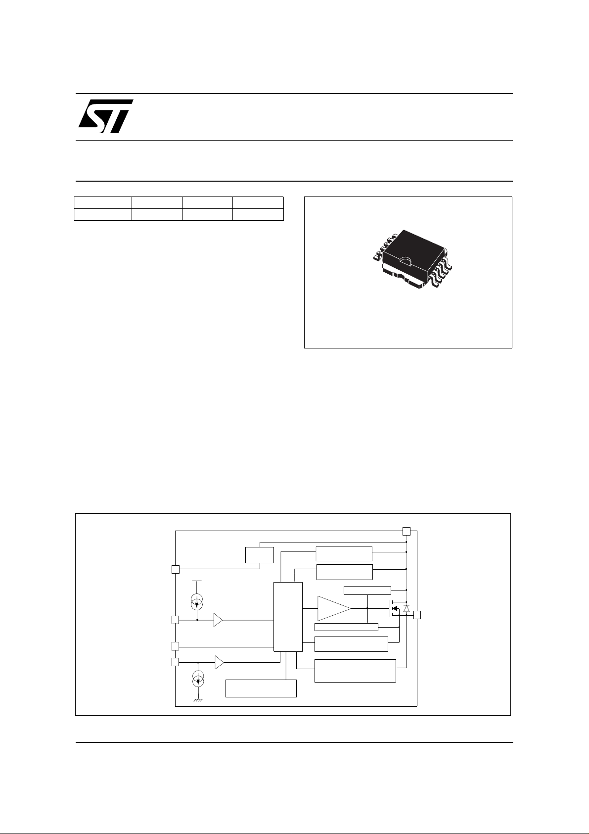
DESCRIPTION
The VN710SP is a mono lithic device m ade using
STMicroelectronics VIPower M0-3 technology,
intended for driving any kind of load with one side
connected to ground. Active VCC pin voltage
clamp protects the device against low energy
spikes (see ISO7637 transients compatibility
table). Active current limitation combined with
thermal shutdown protect the device against
I
OUT
V
CC
VN710S P
PRELIMINARY DATA
10
1
PowerSO-10
overload. Afte r a therma l shutdown eve nt, device
stays latched off and diagnostic stays at a low
level until next falling edge of input signal. The
device detects open load condition both in on
state and off state. Output shorted to VCC is
detected in the off state. Device automatically
turns off in case of ground pin disconnection.
Enable pin allows to switch the device to idle state
with very low quiescent cur rent from VCC. When
enable is low, device tur ns off rega rdless o f input
pin state.
™
BLOCK DIAGRAM
V
CC
V
CC
CLAMP
GND
INPUT
STATUS
ENABLE
(*) See appli c ation schematic at page 7
OVERTEMPERATURE
DETECTION
LOGIC
Octobe r 20 00 1/11
OVERVOLTAGE
DETECTION
UNDERVOLTAGE
DETECTION
Power C LAMP
DRIVER
CURRENT LIMITER
ON STATE OPENLOAD
DETECTION
OFF STATE OPENLOAD
AND OUTPUT SHORTED
TO V
DETECTION
CC
OUTPUT
1
Page 2
VN710SP
THERMAL DATA
Symbol Parameter Value Unit
R
tj-case
R
tj-amb
(*) When mounted on a standard single-sid ed FR-4 board with 50mm2 of Cu (at least 35µm thick).
ABSOLUTE MAXIMUM RATI NG
Symbol Parameter Value Unit
V
CC
-V
-I
GND
I
OUT
-I
OUT
I
IN
I
en
I
STAT
V
ESD
P
T
T
T
stg
Thermal resistance junction-case 1.4 °C/W
(*) Thermal resistance junction-ambient 52 °C/W
DC supply voltage 41 V
Reverse DC suppl y vo lt a ge -0.3 V
CC
Reverse D C ground pin current -200 mA
DC output current Intern ally limited A
Reverse DC output current -35 A
DC input current +/-10 mA
DC enable current +/-10 mA
DC status current +/-1 0 mA
Electrostatic discharge (R=1.5kΩ; C=100pF) 2000 V
Power dissipation at Tc=25°C89W
tot
Junction operating temperature Internally limited °C
j
Case operating temperature -40 to 150 °C
c
Storage te m perature -55 to 150 °C
CONNECTION DIAGRAM (TO P VI EW)
GROUND
ENABLE
STATUS
INPUT
N.C.
V
CC
CURRENT AND VOLTAGE CO NVENTIONS
I
en
V
en
I
IN
V
IN
I
STAT
ENABLE
INPUT
STATUS
10
6
7
8
9
11
GND
5
4
3
2
1
V
CC
OUTPUT
OUTPUT
OUTPUT
OUTPUT
OUTPUT
OUTPUT
I
I
OUT
V
CC
OUT
V
CC
2/11
1
V
STAT
I
GND
Page 3
VN710SP
ELECTRICAL CHARACTERISTICS
(7V<V
<16V; -40°C<Tj<150°C; unless otherwise specified)
CC
POWER
Symbol Parameter Test Conditions Min Typ Max Unit
CC
OV
ON
S
(on)
(off)
Operating supply voltage 5.5 13 16 V
Undervolt age shutdown 345.5V
Overvolt age shutdo wn 16 18 20 V
On state resistance
Supply current
Output current at Turn-off
Off state output current V
Off state output current V
=13V)
CC
Turn-on delay time
Turn-off delay time
/
Turn-on voltage slope
/
Turn-off voltage slope
=15A; Tj=25°C
I
OUT
I
=15A
OUT
Off state; V
=5V
V
IN
Off state; V
VIN=5V; T
On state; VCC=13V; VIN=0V; I
Ven>V
V
CC=VGND
V
IN=Ven
=0V; VIN>V
OUT
=3.5V; VIN>VIH; Ven>V
OUT
enh
=n.c.; V
=13V; Ven=V
CC
=13V; Ven=V
CC
=25°C
j
=16V
OUT
IH
=0V
OUT
OUT
enh
=0V;
=0V;
OUT
RL=0.85Ω, from VIN fallin g edge to
V
=1.3V
OUT
R
=0.85Ω, from VIN rising edge to
L
=11.7V
V
OUT
RL=0.85Ω, from V
V
=10.4V
OUT
RL=0.85Ω, from V
V
=1.3V
OUT
=1.3V to
OUT
=11.7V to
OUT
10
10
=0A;
2.5
050µA
-75 0 µA
40 µs
80 µs
0.1 V/µs
0.1 V/µs
20
40
25
20
4
2mA
V
V
USD
V
R
I
I
LGND
I
L(off1)
I
L(off2)
SWITCHING (V
Symbol Parameter Test Conditions Min Typ Max Unit
t
d(on)
t
d(off )
dV
OUT
dt
dV
OUT
dt
mΩ
mΩ
µA
µA
mA
INPUT PIN (active low)
Symbol Parameter Test Conditions Min Typ Max Unit
IL
IL
IH
IH
ICL
Inpu t low level 1.25 V
Low level input current VIN=1.25V ; Ven>V
enh
-35 µA
Inpu t h igh le v el 3.25 V
High level input current
=3.25V ; Ven>V
V
IN
enh
VIN=3.25V ; Ven=0V -300
-4
-4
Input hysteresis voltage 0.5 V
Inpu t clamp voltag e
I
IN
I
IN
=1mA
=-1mA
66.8
-0.7
8V
V
V
V
I
V
I
I(hyst)
ENABLE PIN (active high)
Symbol Parameter Test Conditions Min Typ Max Unit
enl
Enable low level 1.25 V
Low level enable current Ven=1.25V 4 µA
Enable high level 3.25 V
High level enable curre nt Ven=3.25V 35 µA
Enable hysteresis voltage 0.5 V
Enable clamp voltage
I
en
I
en
=1mA
=-1mA
66.8
-0.7
8V
V
V
I
V
I
V
enl
enh
enh
ehyst
encl
1
µA
µA
V
V
3/11
Page 4
VN710SP
ELECTRICAL CHARACTERISTICS (continued)
STATUS PIN (Open Drain)
Symbol Parameter Test Conditions Min Typ Max Unit
V
STAT
I
LSTAT
C
STAT
V
SCL
Status low output
voltage
Status leakage current Normal operation; V
Status pin input
capacitance
Status clamp voltage
PROTECTIONS
Symbol Parameter Test Conditions Min Typ Max Unit
T
T
t
V
demag
TSD
T
hyst
SDL
I
lim
Shut -do w n t e mp e r at ure 170 190 °C
Reset temperature 135 °C
R
Ther ma l hysteresis 7 15 °C
Overload detection delay Tj>T
Current l imitation 35 55 80 A
Turn-off output clamp
voltage
I
=1.6mA 0.5 V
STAT
=5V 10 µA
STAT
Normal operation; V
=1mA
I
STAT
I
=-1mA
STAT
TSD
I
=2A; VIN=5V; L=6m H VCC-41 VCC-48 VCC-55 V
OUT
=5V 100 pF
STAT
66.8
-0.7
8V
20 µs
V
OPENLOAD DETECTION
Symbol Parameter Test Conditions Min Typ Max Unit
I
OL
Openloa d on state
detection threshold
Openload off state voltage
OL
detection threshold
Openload detection
delay at turn-off
Openload detection
V
t
DOL(off)
t
DOL(on)
delay at turn-on
OPENLOAD STATUS TIMING (with external pull-up)
V
OUT>VOL
V
IN
V
STAT
t
DOL(off)
V
=0V 0.1 1 2 A
IN
VIN=5V 1.5 2.5 3.5 V
500 µs
I
=0V 200 µs
OUT
I
OUT<IOL
t
DOL(on)
V
V
IN
STAT
OVERTEMP STA TUS TIMING
Tj>T
TSD
t
SDL
4/11
2
Page 5

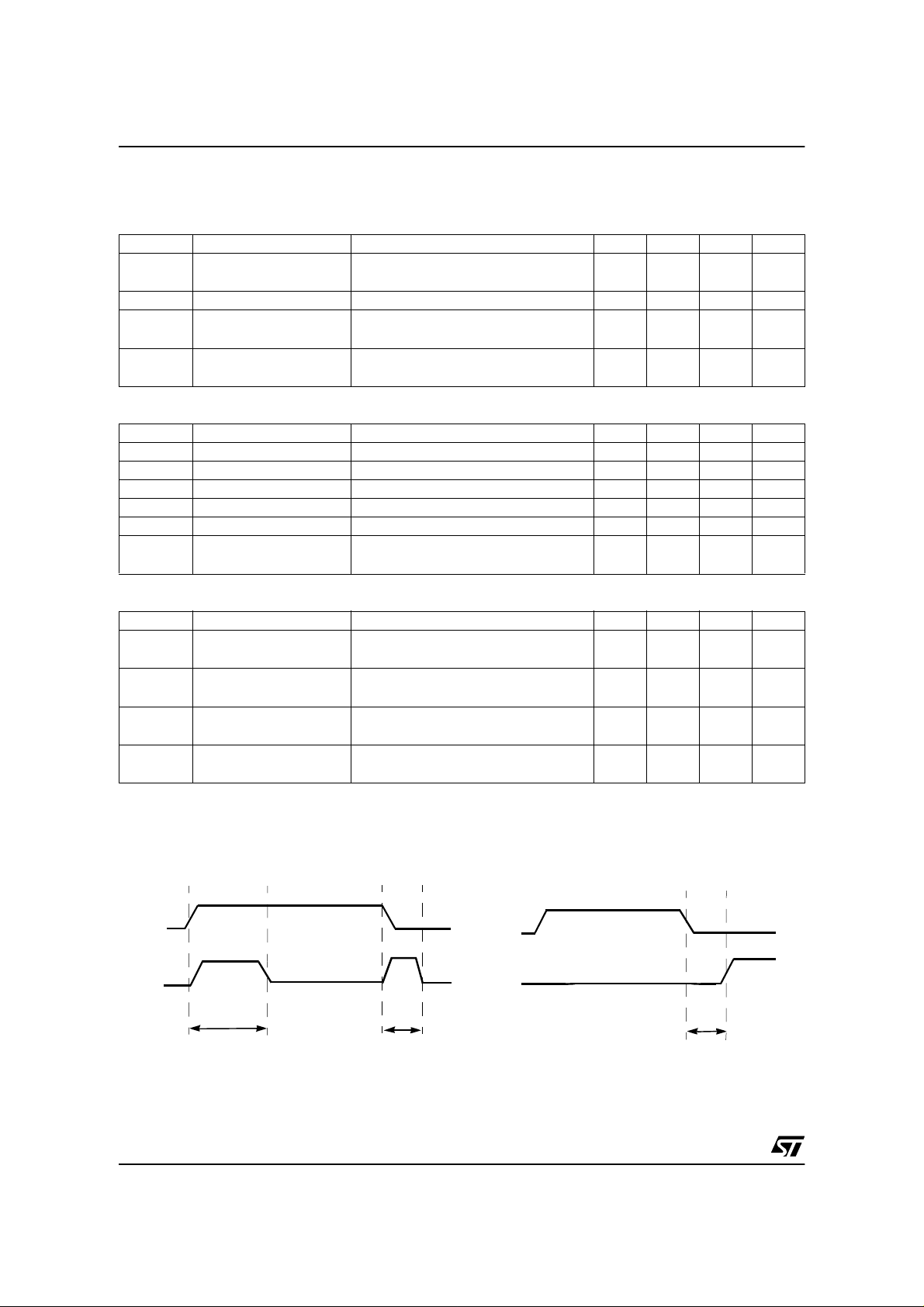
Switching Time Waveforms
V
OUT
dV
/dt
OUT
(on
V
IN
TRUTH TABLE
)
t
d(on)
90%
80%
10%
t
d(off)
dV
OUT
/dt
VN710SP
(off)
t
t
CONDITIONS ENABLE INPUT OUTPUT STATUS
Normal op eration
Current limit ati on
Overtemperature
Undervol tage
Overvoltage
Output voltage > V
Output current < I
Any L X L H
(*) Latched on first overtem perature eve nt; latch cleared on next input falling edge.
OL
OL
H
H
H
H
H
H
H
H
H
H
H
H
H
H
H
L
H
L
L
H
H
L
H
L
H
L
H
L
L
H
L
X
L (*)
L
L
L
L
L
H
H
L
H
H
H
H
H
L (*)
L
X
X
H
H
L
H
H
L
5/11
Page 6
VN710SP
ELECTRICAL TRANSIENTS REQUIREMENTS ON VCC PIN
ISO T/R 7637/1
Test Pul se
I II III IV Delays and Impedance
TEST LEVELS
1 -25V -50V -75V -100V 2ms, 10Ω
2 +25V +50V +75V +100V 0.2ms, 10Ω
3a -25V - 50V -100V -150V 0.1ms, 50Ω
3b +25V +50V +75V +100V 0.1 m s, 50Ω
4 -4V -5V -6V -7V 100ms, 0.01Ω
5 +26.5V +46.5V +66.5V +86.5V 400ms, 2Ω
ISO T/R 7637/1
T e st Pu l s e
IIIIIIIV
TEST LEVELS R ESULT
1 C C C C
2CCCC
3aCCCC
3bCCCC
4CCCC
5CEEE
CLASS CONTENTS
C All func tions of the device are p erformed a s designed after exposure to disturbance.
E
One or more functions of the device is not per formed as designed after exposure and canno t be
returned to proper operation without replacing the device.
SUGGESTED SCHEME FOR ISO TEST PULSE
10KΩ
GND
V
CC
OUTPUT
10KΩ
10KΩ
Warning: Input, Enable, Status Pulled to VCC voltage during
negative transient.
ENABLE
INPUT
STATUS
6/11
from test
generator
open
Page 7

APPLICATION SCHEMATIC
VN710SP
+5V
µ
R
C
R
R
prot
prot
prot
+5V
STA T US
INPUT
ENABLE
GND PROTECTION NETWORK AGAINST
REVERSE BATTERY
Soluti on 1: Resistor in the ground line (R
can be us ed with any type of load.
The fo llowin g is an indica tion on how to dim ension the
resistor.
R
GND
1) R
2) R
where -I
be foun d in the abs olute maximum r ating section of the of
≤ 600mV / (I
GND
≥ (−VCC) / (-I
GND
is the DC re vers e grou nd pi n cu rren t an d can
GND
S(on)ma x
)
GND
).
the devic e’s data sh ee t.
Power Dissipation in R
battery situations) is:
= (-VCC)2/R
P
D
GND
(when VCC<0: during reverse
GND
This resistor can be shared amongst several different
HSD. Please note that the val u e of this resi s to r sh ou l d be
calcul ated with form ula (1) wher e I
sum of the maximum on-state currents of the different
S(on)max
devices.
Please note that if the microprocessor ground is not
common with the device ground then the R
produce a shift (I
and the status output values. This shift will vary
S(on)max
* R
) in the input thresholds
GND
depending on many devices are ON in the case of several
high side drivers sharing the same R
GND
If the calculated power dissipation leads to a large resistor
or several devices hav e to share the sa me resisto r then
the ST suggest to utilize Solution 2 (see belo w).
Solution 2:
A resistor (R
D
GND
A diode (D
=1kΩ) sh ould b e insert ed in paral lel to
GND
if the device will be driving an inductive load.
) in the gr ound line.
GND
only). This
GND
becomes t he
GND
.
will
V
CC
D
OUTPUT
GND
R
V
GND
GND
D
GND
This small signal diode can be safely shar ed amongst
several different HSD. Also in this case, the presence of
j
the ground network wi ll produce a shift (
600mV) in t he
input threshold and the status output values if the
microprocessor ground is not common with the device
ground. This shift will not vary if more than one HSD
shares the same diod e/resisto r network.
LOAD DUMP PROTECTION
Dld is necessary (Transil or MOV) if the load dump peak
voltage exceeds VCC max DC rating. The same applies if
the de vi ce wil l be subj ec t to t rans ie nts on the VCC line that
are great er than th e ones shown i n the ISO T/ R 7637/1
table.
C I/Os PROTECTION:
µ
If a ground protection network is used and negative
transient are pre sent on the VCC line, the control pins will
be pulled negative. ST suggests to insert a resistor (R
in lin e to prevent the µC I/Os pins to latch-up.
The value of these resistors is a compromise between the
leakage c urrent of µC an d the current required by the
HSD I/Os ( Input le vels comp atibilit y) wi th the lat ch-up li mit
of µC I/Os.
≤ R
-V
CCpeak/Ilatchup
Calculation example:
CCpeak
prot
= - 100V an d I
≤ 18.57kΩ.
prot
For V
5kΩ ≤ R
Recommended R
≤ (V
prot
OHµC-VIH-VGND
≥ 20mA; V
latchup
value is10kΩ.
) / I
OHµC
ld
IHmax
≥ 4.5V
prot
)
7/11
1
Page 8

VN710SP
Figure1: Waveforms
INPUT
LOAD VOLTAGE
STATUS
V
CC
INPUT
LOAD VOLTAGE
STATUS
NORMAL OPERATION
UNDERVOLT AGE
V
USDhyst
V
USD
undefined
V
CC
INPUT
LOAD VOLTAGE
STATUS
INPUT
LOAD VOLTAGE
STATUS
ENABLE
T
j
INPUT
LOAD CURRENT
STATUS
VCC<V
V
OV
OV
VCC>V
V
OV
OVhyst
OPENLOAD
OVERVOLTAGE
t
DOL(on)
t
DOL(on)
OVERTEMPERATURE
T
TSD
T
R
8/11
1
INPUT
LOAD VOLTAGE
STATUS
SHOR T T O V
undefined undefined
t
DOL(off) t
CC
DOL(off)
1
Page 9

PowerSO-10™ MECHANICAL DATA
VN710SP
DIM.
MIN. TYP MAX. MIN. TYP. MAX.
mm. inch
A 3.35 3.65 0.132 0.144
A (*) 3.4 3.6 0.134 0.142
A1 0.00 0.10 0.000 0.004
B 0.40 0.60 0.016 0.024
B (*) 0.37 0.53 0.014 0.021
C 0.35 0.55 0.013 0.022
C (*) 0.23 0.32 0.009 0.0126
D 9.40 9.60 0.370 0.378
D1 7.40 7.60 0.291 0.300
E 9.30 9.50 0.366 0.374
E2 7.20 7.60 0.283 300
E2 (*) 7.30 7.50 0.287 0.295
E4 5.90 6.10 0.232 0.240
E4 (*) 5.90 6.30 0.232 0.248
e 1.27 0.050
F 1.25 1.35 0.049 0.053
F (*) 1.20 1.40 0.047 0.055
H 13.80 14.40 0.543 0.567
H (*) 13.85 14.35 0.545 0.565
h 0.50 0.002
L 1.20 1.80 0.047 0.070
L (*) 0.80 1 .10 0.031 0.043
α 0º 8º 0º 8º
α (*) 2º 8º 2º 8º
(*) Muar only POA P013P
HE
h
A
F
A1
10
1
eB
0.25
D
= =
D1
= =
E2
DETAIL "A"
DETAIL "A"
B
0.10 A
E
SEATING
PLANE
A
C
α
B
E4
SEATING
PLANE
A1
L
P095A
9/11
11
1
1
1
Page 10

VN710SP
PowerSO-10™ SUGGESTED PAD LAYOUT
14.6 - 14.9
10.8 - 11
6.30
0.67 - 0.73
1
2
3
9.5
4
5
10
0.54 - 0.6
9
8
7
1.27
6
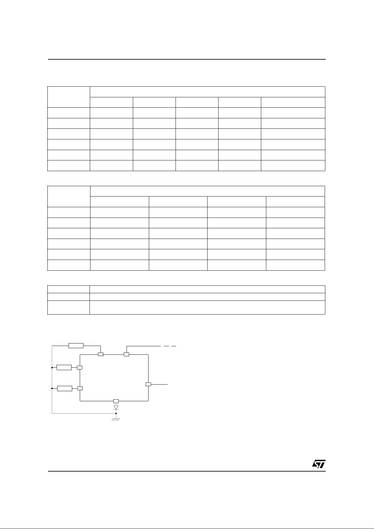
TAPE AND REEL SHIPMENT (suf fix “13TR”)
TUBE SHIPMENT (no suffix)
C
A
B
A
All dimensi ons ar e in mm.
Base Q.ty Bulk Q.ty Tube length (± 0.5) A B C (± 0.1 )
Casablanca 50 1000 532 1 0.4 16. 4 0.8
Muar 50 1000 532 4.9 17.2 0.8
MUARCASABLANCA
B
REEL DIMENSIONS
Base Q.ty 600
Bulk Q.ty 600
A (max) 330
B (min) 1.5
C (± 0.2) 13
F 20.2
G (+ 2 / -0) 24.4
N (min) 60
T (max) 30.4
C
TAPE DIMENSIONS
According to Electronic Industries Association
(EIA) Standard 481 rev. A, Feb 1986
Tape width W 24
Tape Hole Spacing P0 (± 0.1) 4
Component Spacing P 24
Hole Diameter D (± 0.1/-0) 1.5
Hole Diameter D1 (min) 1.5
Hole Position F (± 0.05) 11.5
Compartm ent Depth K (max) 6.5
Hole Spacing P1 (± 0.1) 2
All dimensions are in mm.
Top
cover
tape
End
500mm min
All dimensions are in mm.
Empty components pockets
saled with cover tape.
User direction of feed
Start
No componentsNo components Componen ts
500mm min
10/11
1
1
Page 11

VN710SP
Information furnished is believed to be accurate and r eliable. Ho wev er, STMicroelectr onics assume s no r es ponsibility for the consequenc es
of use of such information nor for any infringement of patents or other rights of third parties which may results from its use. No license is
granted by implication or otherwise under a ny patent or patent rights of STMicroelectronics. Specif ic ations mentioned in this publication are
subject to c hange withou t notice. This publication supersed es and replace s all information previous ly s upplied. ST M icroelect r on ics products
are not authorized for use as critical components in life support devices or systems without express written approval of STMicroelectronics.
Australia - Brazil - China - Finland - France - Germany - Hong Kong - India - Italy - Japan - Malaysia - Malta -
Morocco - Singapore - Spain - Sweden - Switzerland - United Kingdom - U.S.A.
The ST logo is a regi s tered trademark of STMicroelectronic s
2000 STMicroelectronics - Printed in ITALY- All Rights Reserved.
STMicroelectronics GROUP OF COMPANIES
http://www.st.com
11/11
 Loading...