

Page 1

VN460SP
SINGLE CHANNEL HIGH SIDE SMART
SOLID STATE RELAY
TYPE V
VN460SP VCC-55V 20 m Ω 25 A 36 V
■ OUTPUTCURRENT(CONTINUOUS):
25 A @ T
■ 5 V LOGICLEVELCOMPATIBLEINPUT
■ UNDERVOLTAGE SHUT-DOWN
■ OVERVOLTAGE SHUT-DOWN
■ THERMALSHUT-DOWN
■ OPENDRAIN DIAGNOSTIC OUTPUT
■ VERY LOW STAND-BY POWER
dema g
=25oC
C
R
DS(on)
IOUT V
CC
DISSIPATION
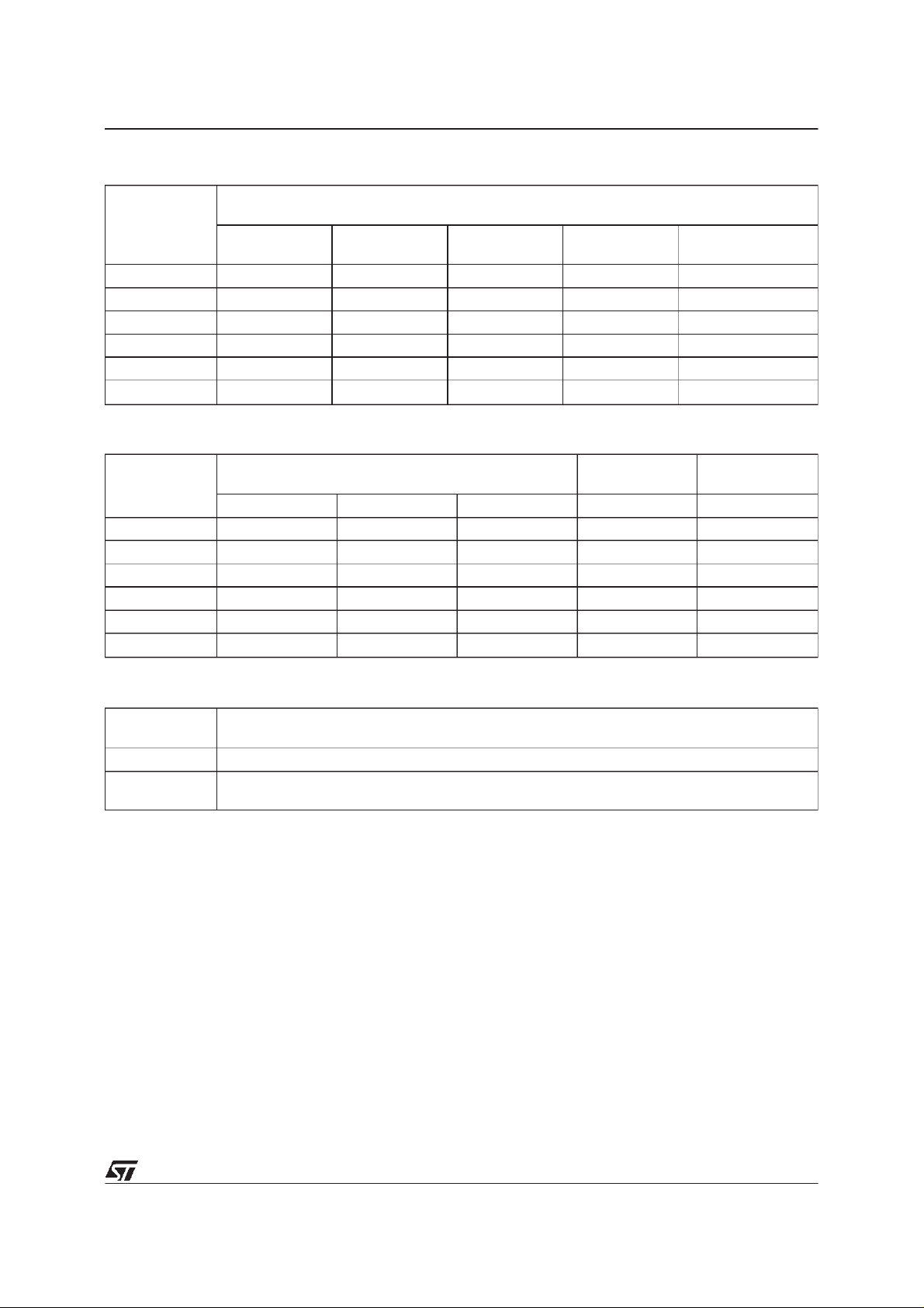
DESCRIPTION
The VN460SP is a monolithic device made using
SGS-THOMSON Vertical Intelligent Power
Technology, intended for driving resistive or
inductive loads with one side connected to
ground.
Built-in thermal shut-down protects the chip from
over temperature and shortcircuit.
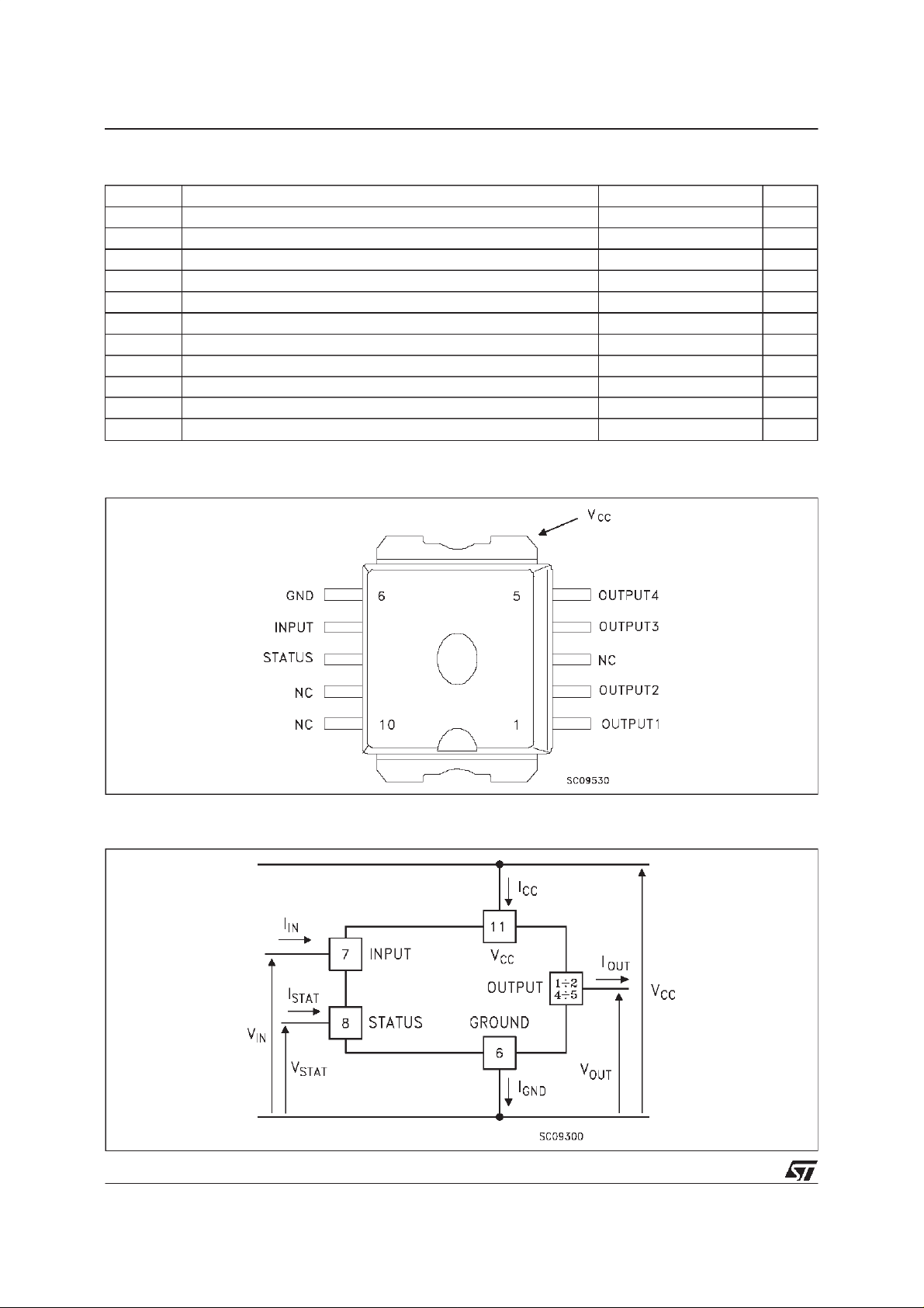
BLOCK DIAGRAM
10
1
Power SO-10
TM
The control input is 5V CMOS logic level
compatible.
The open drain diagnostic output indicates open
circuit(no load) and overtemperaturestatus.
June 1998
1/9
Page 2
VN460SP
ABSOLUTEMAXIMUMRATING
Symb o l Para met er Val u e Uni t
V
-V
I
OUT
I
I
I
STAT
-I
GND
V
ESD
P
T
T
CONNECTION DIAGRAM
Power Supply Voltage (continuous ) 45 V
CC
Revers e Su pply Voltage (continuous) -0. 3 V
CC
Out put Current (continuous ) Int ernally Limited A
Reverse Output Current -25 A
R
Input Current ±10 mA
IN
St at us Pin Curr ent ±10 mA
Reverse Ground Current -200 mA
Elect r o st at ic Discharge (1.5 kΩ, 100 pF ) 2000 V
Power Dissipation at Tc≤ 25oC112W
tot
Junction Operatin g Tempe rat ure -40 to 150
j
St orage Temperat ure -55 to 150
stg
o
C
o
C
CURRENT AND VOLTAGE CONVENTIONS
2/9
Page 3
ELECTRICALTRANSIENTS REQUIREMENTS
VN460SP
ISO T/ R
7637/1
Test Puls e
1 -25 V -50 V -75 V -100 V 2 ms , 10 Ω
2 +2 5 V +50 V +75 V +100 V 0.2 m s , 10 Ω
3a -25 V - 50 V -100 V -150 V 0.1 µs, 50 Ω
3b +25 V +50 V +75 V +100 V 0.1 µs, 50 Ω
4 -4 V -5 V -6 V -7 V 100 ms, 0.0 1 Ω
5 +26. 5 +46. 5 +66.5 +86.5 400 ms , 2 Ω
ISO T/ R
7637/1
Test Puls e
1C C C C
2C C C C
3a C C C C
3b C C C C
4C C C C
5C E E E
(With a series resistor ≥ 1KΩin input and status pins).
I II II I IV Delays and
TEST L EVE LS RESUL TS
I II III IV
TEST LEVEL S
Impedance
CLAS S CONTENTS
C All f unction of the device ar e per f ormed as d esigne d aft er exposure to disturbanc e.
E O ne or m or e functions of the device is not per formed a s desig ned af ter exposure and
cannot be returned t o proper oper a t ion withou t r eplacing the dev ic e.
3/9
Page 4

VN460SP
THERMALDATA
R
thj-case
R
thj-a(∗)
(∗) When mounted using minimum recommended pad size on FR-4 board.
Ther mal Resis t ance Junc t io n- case Max 1.1
Ther mal Resis t ance Junc t io n- ambien t Max 50
ELECTRICAL CHARACTERISTICS (VCC=13 V; -40oC<TJ< 125oC unlessotherwisespecified)
POWER
Symbol Parameter Test Conditions Min. Typ. Max. Unit
V
Oper at i ng S u pply
CC
5.5 13 36 V
Volt age
V
Under V ol ta ge S hut
usd
345.5V
Down
V
R
I
Ov ervoltage Shut Down 36 39 45 V
ov
On State Re sis t a nce I
on
Supply Current Of f stat e T
S
=5A TJ=25oC
OUT
=5A
I
OUT
On State
Case
=25oC
15
1.4
3.3
LOGIC INPUT
o
o
20
36
30
C/W
C/W
mΩ
mΩ
µA
mA
Symbol Parameter Test Conditions Min. Typ. Max. Unit
V
Input Low Lev el
IL
(*) 1.5 V
Volt age
V
Input High Level
IH
(*) 3.5 V
Volt age (see not e 1)
V
I(hyst.)
Input Hysteresis
0.2 0. 85 1.5 V
Volt age
I
V
(*) : The input voltage is internally clamped at 6V about. Itis possible to connect this pin to an higher voltagevia an external resistor
provided the input current doesnotexceed 10 mA.
Input Current VIN=5V T
IN
Input Clamp Volt age IIN=10mA
ICL
=-10mA
I
IN
=25oC100µA
case
56
7V
-0.7
SWITCHING(VCC=13V)
Symbol Parameter Test Conditions Min. Typ. Max. Unit
t
d(on)
t
r
t
d(off)
t
f
(di/dt)
(di/dt)
Turn-on Delay Time Of
Out put Current
Rise Time Of Output
Current
Turn-off Delay Time Of
Out put Current
Fall T ime Of Output
Current
Tur n-on Current Slope I
on
Tur n-of f C urr ent Slope I
off
I
= 5 A Resistive Load
OUT
Input Rise Time < 0. 1 µsT
I
= 5 A Resistive Load
OUT
Input Rise Time < 0. 1 µsT
I
= 5 A Resistive Load
OUT
Input Rise Time < 0. 1 µsT
I
= 5 A Resistive Load
OUT
Input Rise Time < 0. 1 µsT
=5A 0.02 0.05 A/µs
OUT
=5A 0.02 0.05 A/µs
OUT
=25oC
j
=25oC
j
=25oC
j
=25oC
j
25 90 250 µs
80 300 650 µ s
300 750 1500 µs
80 200 400 µ s
V
4/9
Page 5

VN460SP
ELECTRICAL CHARACTERISTICS (continued)
PROTECTIONS AND DIAGNOSTICS
Symbol Parameter Test Conditions Min. Typ. Max. Unit
T
TSD
T
T
RSD
(HYST)
V
ENOL
I
OL
I
OV
I
AV
V
STAT
V
SCL
t
POL
t
POVL
V
DEMAG
(∗) ISO definitions T
Ther mal Shut -down
150 170 190
Tem perature
TR
Ther mal Reset
135
Tem perature
Thermal Hyst eresis 5 15 50
Out put V o lt age
8V≤ VCC≤30V 5.2 6.6 8 V
Aut horizing Openl oad
Detection
Open Loa d Cur rent
8V≤ VCC≤30V 100 800 1500 m A
Level
Over Current R
Aver age Curre nt in
Short Circuit
St at us Output Volt age I
St at us Cl amp V olt age I
≤10 mΩ
LOAD
o
C<T
-40
R
LOAD
=85oC
T
C
= 1.6 mA (Fault Condition) 0.4 V
STAT
=10mA
STAT
=-10mA
I
STAT
Case
≤10 mΩ
<125oC
25 50 A
5.4 A
5.5 6
7V
-0.7
St at us De lay (∗) 50 300 9 50 µs
St at us De lay (∗)10µs
Tur n-of f O utput Clamp
I
=5A, L=1mH, VIN=0 VCC-45 VCC-50 VCC-55 V
OUT
Volt age
= Status delay in case of open load conditions
POL
= Status delay in case of over load conditions
T
POVL
o
C
o
C
o
C
V
5/9
Page 6

VN460SP
FIGURE 1
SWITCHING PARAMETERSTEST CONDITIONS
TRUTH TABLE
Conditions INPUT OUTPUT STAT US
Normal Oper a ti on L
H
Ov er- voltage X L H
Under-voltage X L H
Ther mal s hut-down H L L
Open load H H L
H = high level, L= low le v el, X= unspecified
6/9
L
H
H
H
Page 7

FIGURE2: SwitchingWaveforms
VN460SP
7/9
Page 8

VN460SP
PowerSO-10MECHANICAL DATA
DIM.
mm inch
MIN. TYP. MAX. MIN. TYP. MAX.
A 3.35 3.65 0.132 0.144
A1 0.00 0.10 0.000 0.004
B 0.40 0.60 0.016 0.024
c 0.35 0.55 0.013 0.022
D 9.40 9.60 0.370 0.378
D1 7.40 7.60 0.291 0.300
E 9.30 9.50 0.366 0.374
E1 7.20 7.40 0.283 0.291
E2 7.20 7.60 0.283 0.300
E3 6.10 6.35 0.240 0.250
E4 5.90 6.10 0.232 0.240
e 1.27 0.050
F 1.25 1.35 0.049 0.053
H 13.80 14.40 0.543 0.567
h 0.50 0.002
L 1.20 1.80 0.047 0.071
q 1.70 0.067
α 0
o
o
8
==
==
HE
h
A
F
A1
610
51
eB
M
0.25
D
==
D1
==
DETAIL”A”
E2
==
DETAIL”A”
Q
B
0.10 A
E1E3
==
SEATING
PLANE
A
C
α
B
E4
==
SEATING
PLANE
A1
L
==
0068039-C
8/9
Page 9

VN460SP
Information furnished is believed tobe accurate and reliable. However, STMicroelectronics assumes no responsibility for theconsequences
of use of such information nor for any infringement of patents or other rights of third parties which may result from its use. No license is
granted by implication orotherwise under any patent or patent rights of STMicroelectronics. Specification mentioned in this publication are
subject tochangewithoutnotice. This publication supersedes andreplaces all information previously supplied.STMicroelectronics products
are not authorized for use as critical componentsin lifesupport devices or systems without express written approval of STMicroelectronics.
Australia -Brazil - Canada- China - France- Germany- Italy- Japan - Korea- Malaysia -Malta - Mexico - Morocco - TheNetherlands -
Singapore- Spain- Sweden- Switzerland- Taiwan -Thailand - United Kingdom- U.S.A.
The ST logo isa trademarkof STMicroelectronics
1998 STMicroelectronics– Printed in Italy–AllRights Reserved
STMicroelectronicsGROUP OF COMPANIES
.
9/9
 Loading...