

Page 1
VN450
THREE CHANNELS HIGH SIDE SMART
SOLID STATE RELAY
TYPE Channe l R
VN450 1 & 2340 m Ω
■ OUTPUTCURRENT(CONTINUOUS):
DS(on)
300 m Ω
10 A (CHANNEL 1,2) @ T
2 A (CHANNEL 3) @T
■ 5 V LOGIC LEVELCOMPATIBLEINPUTS
■ UNDERVOLTAGE SHUT-DOWN
■ OVERVOLTAGE SHUT-DOWN
■ THERMALSHUT-DOWN
■ OPENDRAIN DIAGNOSTIC OUTPUTS
■ VERY LOW STAND-BY POWER
I
10 A
=25oC
C
=25oC
C
OUT
2A
V
CC
36 V
36 V
DISSIPATION
DESCRIPTION
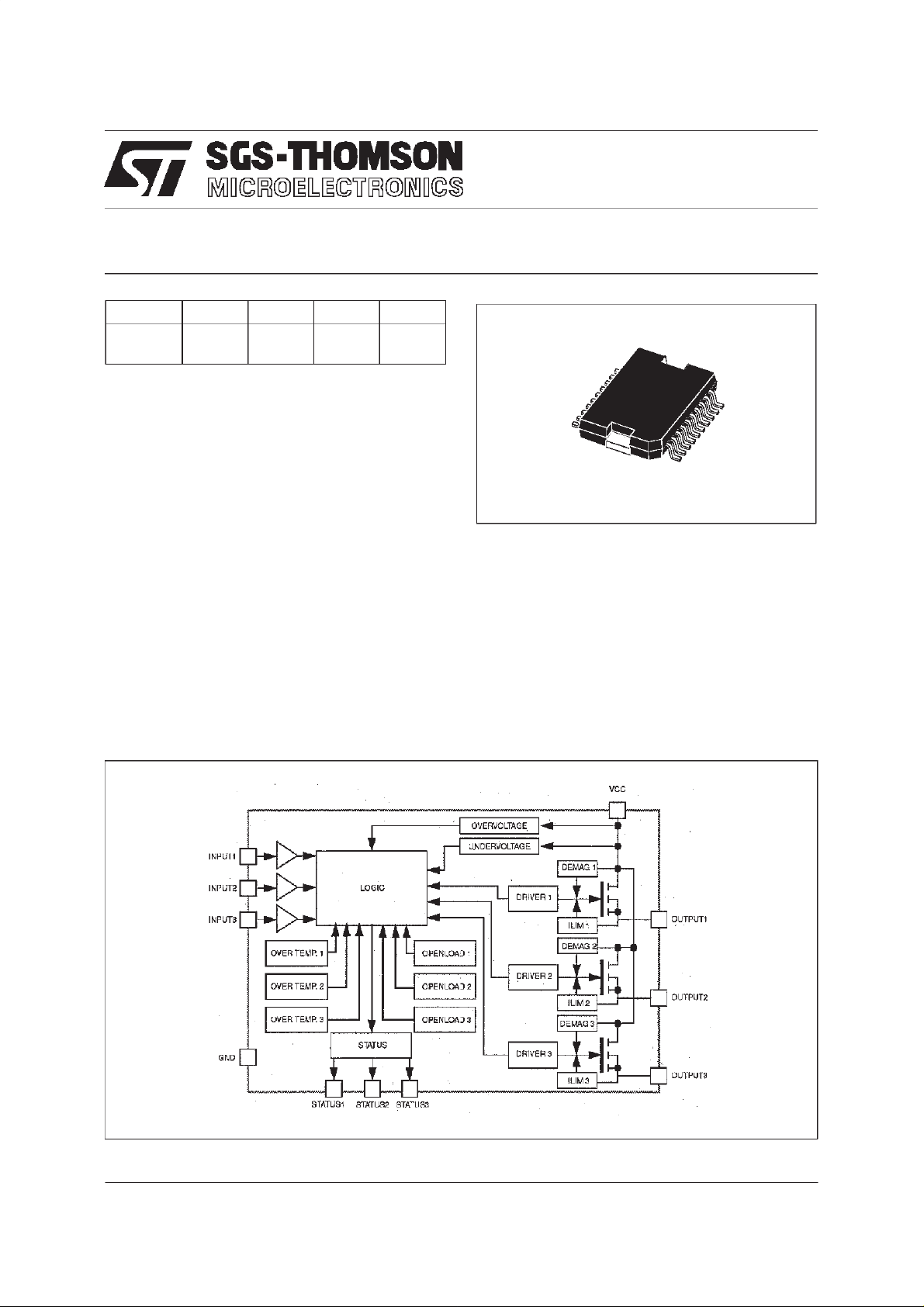
The VN450 is a monolithic device made using
SGS-THOMSON Vertical Intelligent Power
Technology, intended for driving resistive or
inductive loads with one side connected to
ground. This device has three independant
channelsand threediagnostics.
BLOCK DIAGRAM
Power SO-20
TM
Built-in thermal shut-down protects the chip from
over temperatureand short circuit.
The control inputs are 5V CMOS logic level
compatible.
The open drain diagnostic outputs indicate short
circuit(no load) and overtemperaturestatus.
February 1998
SC09570
1/9
Page 2
VN450
ABSOLUTEMAXIMUMRATING
Symb o l Para met er Val u e Uni t
V
-V
-I
I
OUT 1,2
I
OUT 3
I
R1,2
I
R3
I
IN 1,2 ,3
I
STAT 1 ,2, 3
V
ESD
P
T
T
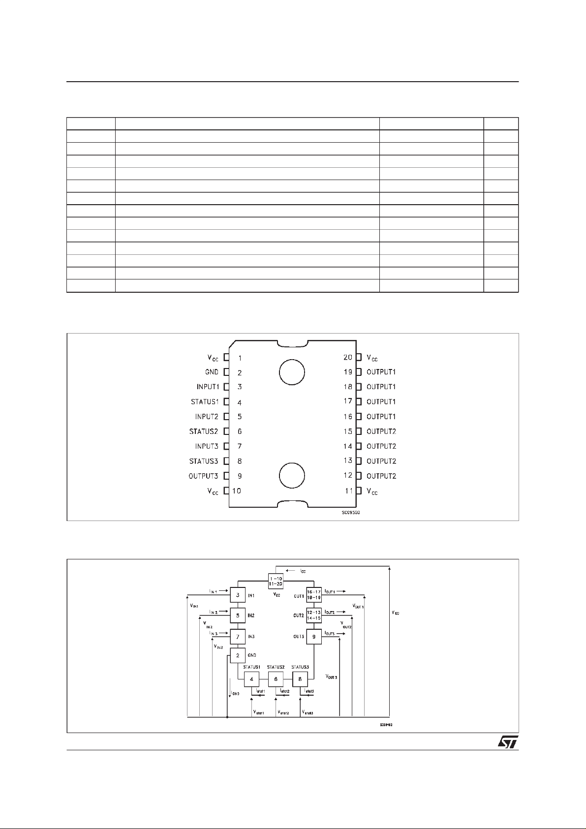
CONNECTION DIAGRAM
Supply V olt a ge ( con ti nuous ) 45 V
CC
Reverse Supply V olt ag e (cont i nuous) -0. 3 V
CC
Reverse Ground Current -200 mA
gnd
Out put Curr ent (cont inuou s) , channels 1, 2 10 A
Out put Curr ent (cont inuou s) , channel 3 2.5 A
Reverse Outp ut Current (c ontinuous) channels 1, 2 -10 A
Reverse Outp ut Current (c ontinuous) channel 3 -2. 5 A
Input Current ±10 mA
Status Output Current ±10 mA
Electrostatic Discharge (R=1.5 kΩ, C=100 pF) 2000 V
Power Dis sipation at Tc≤ 25oC95W
tot
Junct ion Opera t ing T emperature -40 t o 150
j
Sto rage T emperat ur e -55 t o 150
stg
o
C
o
C
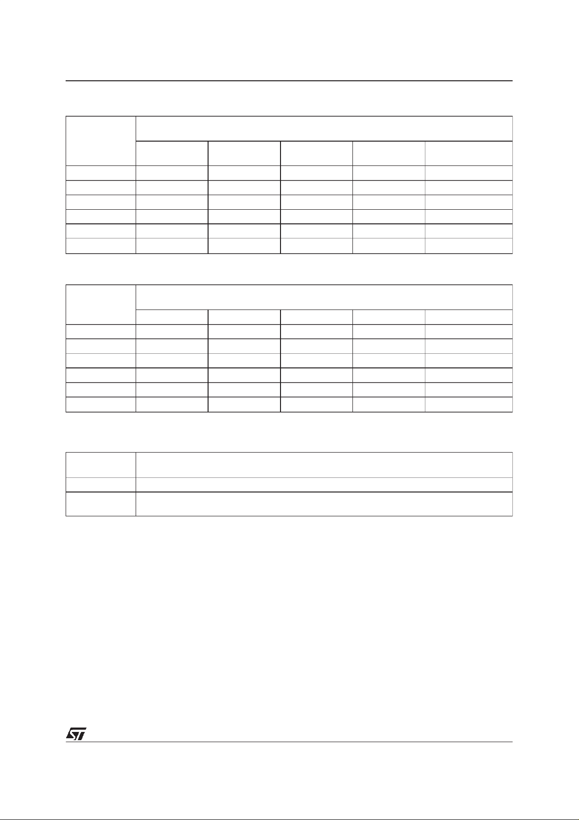
CURRENT AND VOLTAGE CONVENTIONS
2/9
Page 3
ELECTRICALTRANSIENTS REQUIREMENTS
VN450
ISO T/ R
7637/1
Test Pulse
1 -25 V -50 V -75 V -100 V 2 ms , 10 Ω
2 +2 5 V +5 0 V + 75 V +100 V 0.2 m s, 10 Ω
3a -25 V -50 V -100 V -150 V 0.1 µs, 50 Ω
3b +25 V +50 V +75 V +100 V 0.1 µs, 50 Ω
4 -4 V -5 V -6 V - 7 V 100 ms, 0.0 1 Ω
5 +26.5 V +46. 5 V + 66.5 V +86. 5 V 400 ms, 2 Ω
ISO T/ R
7637/1
Test Pulse
1CCCC
2CCCC
3aCCCC
3bCCCC
4CCCC
5CEEE
(With a series resistor ≥ 1KΩin input and status pins).
I II II I IV Delays and
IIIIIIIV
TEST LEVEL S
Impedance
TEST LEVELS RESULTS
CLAS S CONTENTS
C All f unction of the dev ice are per f ormed as designe d afte r exposur e to distu rbance.
E O ne or m or e functions of t he device is not perfor med as desig ned af ter exposure and
cannot be retu rned t o pr op er operation without replacing the device.
3/9
Page 4

VN450
THERMALDATA
R
thj-case
R
thj-amb
Thermal Resistance Junction-case (1) Max 1.3
Ther mal Resis t ance Junct io n- ambien t Max 50
ELECTRICAL CHARACTERISTICS (VCC=13 V; -40oC<Tj<125oC unless otherwisespecified)
POWER
Symbol Parameter Test Conditions Min. Typ. Max. Un it
V
V
V
R
I
Oper at i ng S u pply
CC
5.5 13 36 V
Volt age
usd
Under Voltage
345.5V
Shut-Down
Ov ervoltage S hut - D own 36 39 45 V
ov
On Stat e Resist a nce I
on
I
I
I
Supply Current Of f stat e T
S
On state
=2A Tj=25oC
OUT 1,2
=2A
OUT 1,2
=0.5A Tj=25oC
OUT 3
= 0.5 A
OUT 3
case
=25oC
30
4.2
300
540
o
o
40
75
60
10
C/W
C/W
mΩ
mΩ
mΩ
mΩ
µA
mA
LOGIC INPUT (Channel1,2,3)
Symbol Parameter Test Conditions Min. Typ. Max. Un it
V
Input Low Level
IL
(*) 1.5 V
Volt age
V
Input Hig h Lev el
IH
(*) 3.5 V
Volt age (see note 1)
V
I(hyst.)
Input Hysteresis
0.2 0.85 1.5 V
Volt age
I
V
(*) : The input voltage is internally clamped at 6V about. Itis possible to connect this pin to an higher voltage via an external resistor
provided the input current does not exceed 10 mA.
Input Current VIN=5V T
IN
Input Cla m p Volt ag e IIN=10mA
ICL
=-10mA
I
IN
=25oC100µA
case
56
7V
-0.7
SWITCHING(VCC=13V;Tj=25oC; input rise time < 0.1µs)
Symbol Parameter Test Conditions Min. Typ. Max. Un it
t
d(on)
t
t
d(off)
t
di/dt
di/dt(
Turn-on Delay Time Of
Out put Cu r rent
Rise Time Of Output
r
Current
Turn-off Delay Time Of
Out put Cu r rent
Fall T ime Of Output
f
Current
Tur n-on Current Slope R1=6.5Ω Channe ls 1,2
(on)
Tur n-of f C urrent Slope R1=6.5Ω Channe ls 1,2
off)
R1=6.5Ω Channe ls 1,2
=26Ω C hannels 3
R
1
R1=6.5Ω Channe ls 1,2
=26Ω C hannels 3
R
1
R1=6.5Ω Channe ls 1,2
=26Ω C hannels 3
R
1
R1=6.5Ω Channe ls 1,2
=26Ω C hannels 3
R
1
=26Ω C hannels 3
R
1
=26Ω C hannels 3
R
1
10
2
32
8
40
20
150
20
12030300
75
32
8
80
20
0.02
0.02
0.02
0.02
140
70
300
60
600
150
160
50
0.05
0.05
0.05
0.05
V
µs
µs
µs
µs
µs
µs
µs
µs
A/µs
A/µs
A/µs
A/µs
4/9
Page 5

VN450
ELECTRICAL CHARACTERISTICS (continued)
PROTECTIONS AND DIAGNOSTICS
Symbol Parameter Test Conditions Min. Typ. Max. Un it
T
TSD
T
T
RSD
(HYST)
V
ENOL
I
OL
I
OV
I
AV
V
STAT 1 ,2,3
V
SCL1,2,3
t
POL
t
POVL
V
DEMAG
(∗) ISO definitions T
Ther mal Shut-d own
150 170 190
Tem perature
TR
Ther mal Reset
135
Tem perature
Thermal Hysteresis 5 1 5 30
Out put Voltage
8V ≤ VCC ≤ 36V 5.2 6.6 8 V
Aut horizing O penl oad
Detection
Open Load Cur rent
Level
Over Current R1≤10 mΩ c hannel s 1,2
Aver age Current in
Short Circuit
St at us O ut put Volt a ge I
St at us Clam p Volt age I
Channels 1,2 8V ≤ VCC≤ 18 V
Channels 3 8V ≤ V
≤10 mΩ c hannel 3
R
1
R1≤10 mΩ T
Ca se
CC
=85oC
≤ 30 V
channels 1,2
channel 3
= 1.6 mA (Faul t Condition) 0.4 V
STAT
=10mA
STAT
I
=-10mA
STAT
1005450
50
10
2
18
3.5
3.4
2
5.5 6
-0.7
St at us Delay (∗) (s e e f igure 1) 50 300 950 µ s
St at us Delay (∗) (see f igure 1) 10 µs
Tur n-of f O utput Cl amp
Volt age
= Statusdelay in case of open load conditions
POL
T
= Status delay in case of over load conditions
POVL
I
=2A L=1mH V
OUT 1
=2A L=1mH V
I
OUT 2
= 0.5 A L = 1 mH V
I
OUT 3
IN1
IN2
IN3
=0
=0
=0
V
-45 VCC-50 VCC-55 V
CC
800
100mAmA
7V
o
C
o
C
o
C
A
A
A
A
V
5/9
Page 6

VN450
FIGURE 1
SWITCHING PARAMETERS TESTCONDITIONS
TRUTH TABLE (Channels 1,2,3)
Conditions INPUT OUTPUT STATUS
Normal Opera ti on L
H
Ov er- voltage X L H
Under-voltage X L H
Ther mal s hut-down H L L
Open load H H L
H = high level, L= low level, X = unspecif ie d
6/9
L
H
H
H
Page 7

FIGURE2: SwitchingWaveforms
VN450
7/9
Page 8

VN450
PowerSO-20MECHANICAL DATA
DIM.
MIN. TYP. MAX. MIN. TYP. MAX.
mm inch
A 3.60 0.1417
a1 0.10 0.30 0.0039 0.0118
a2 3.30 0.1299
a3 0 0.10 0 0.0039
b 0.40 0.53 0.0157 0.0209
c 0.23 0.32 0.009 0.0126
D (1) 15.80 16.00 0.6220 0.6299
E 13.90 14.50 0.5472 0.570
e 1.27 0.050
e3 11.43 0.450
E1 (1) 10.90 11.10 0.4291 0.437
E2 2.90 0.1141
G 0 0.10 0 0.0039
h 1.10 0.0433
L 0.80 1.10 0.0314 0.0433
N10
S8
o
(max.)
o
(max.)
T 10.0 0.3937
(1) ”D and E1” do notinclude moldflash or protusions
- Mold flashor protusions shallnot exceed 0.15mm (0.006”)
NN
R
8/9
E2
hx45°
a2
A
b
DETAILA
110
e3
D
T
e
1120
DETAILB
E1
PSO20MEC
lead
a3
Gage Plane
E
DETAILB
0.35
S
a1
L
c
DETAILA
slug
-C-
SEATING PLANE
GC
(COPLANARITY)
0056635
Page 9

VN450
Information furnished is believed to be accurate and reliable. However, SGS-THOMSON Microelectronics assumes no responsability for the
consequences of use of such information nor for any infringement of patents or other rights of third parties which may resultsfrom its use. No
license is granted by implication or otherwise under anypatent orpatent rights of SGS-THOMSON Microelectronics. Specifications mentioned
in this publication are subject to change without notice. This publication supersedes and replaces all information previously supplied.
SGS-THOMSON Microelectronicsproducts are notauthorized for useas critical componentsin life supportdevices or systems without express
written approval ofSGS-THOMSON Microelectonics.
1998 SGS-THOMSON Microelectronics - Printed in Italy - All Rights Reserved
Australia - Brazil - Canada - China - France - Germany- Italy - Japan - Korea - Malaysia - Malta - Morocco - The Netherlands -
Singapore - Spain- Sweden - Switzerland - Taiwan - Thailand - United Kingdom - U.S.A
SGS-THOMSON Microelectronics GROUP OF COMPANIES
...
9/9
 Loading...