

Page 1

VN410
SMART DIRECTION INDICATOR
2 CHANNEL DRIVERS
TYPE V
VN41 0 60V 4.8 A 0.07 Ω
In(✬) : ISO definition nominal current for high side automotive
switches.
■ LOADCURRENT UP TO 15A PER CHANNEL
■ OVERVOLTAGEPROTECTION
■ UNDERVOLTAGE PROTECTION
■ DOUBLE FLASHINGFREQUENCY IN LOW
DSS(cl)
In(✬ )R
on
LOADCONDITION
■ CYCLEBY CYCLEPOWERLIMITATION
■ BUZZER DRIVER
■ TRAILERINDICATION
DESCRIPTION
The VN410 is a monolithic device made using
SGS-THOMSON Vertical Intelligent Power
Technology,integrating all the featuresneeded to
implement a complete automotive flashing
system.
This device has two identical power channels, so
the informations are are specified for only one. R
pins are connected to an external R, C
C
t
networkwhich fixes the flashing frequency.LDIR,
RDIR direction inputs activate the corresponding
output (or none). EM inputs turns on both power
outputs for emergency flashing, which is reflected
MULTIWATT-15
Order Codes :
(vertical) (In Line)
VN410 VN410(012Y)
by flashing red LED connected to LEDEM output.
AL input can be connectedto an anti-theft alarm
system, making both power outputs flashing. In
case of low load (burned lamp) buzzer frequency
and outputs flashing will double, thus indicating a
fault condition(directionmode only).
In case of overloading of the power outputs,
built-in-thermalshutdown circuits will reduce duty
,
cycle so as to keep maximum junction
t
temperature within safe limits. Rol pin is
connected to an external resistor to detect a
burned lamp and a trailer connection. LEDT is
connected to an external green LED which
indicatesthe trailerconnection.
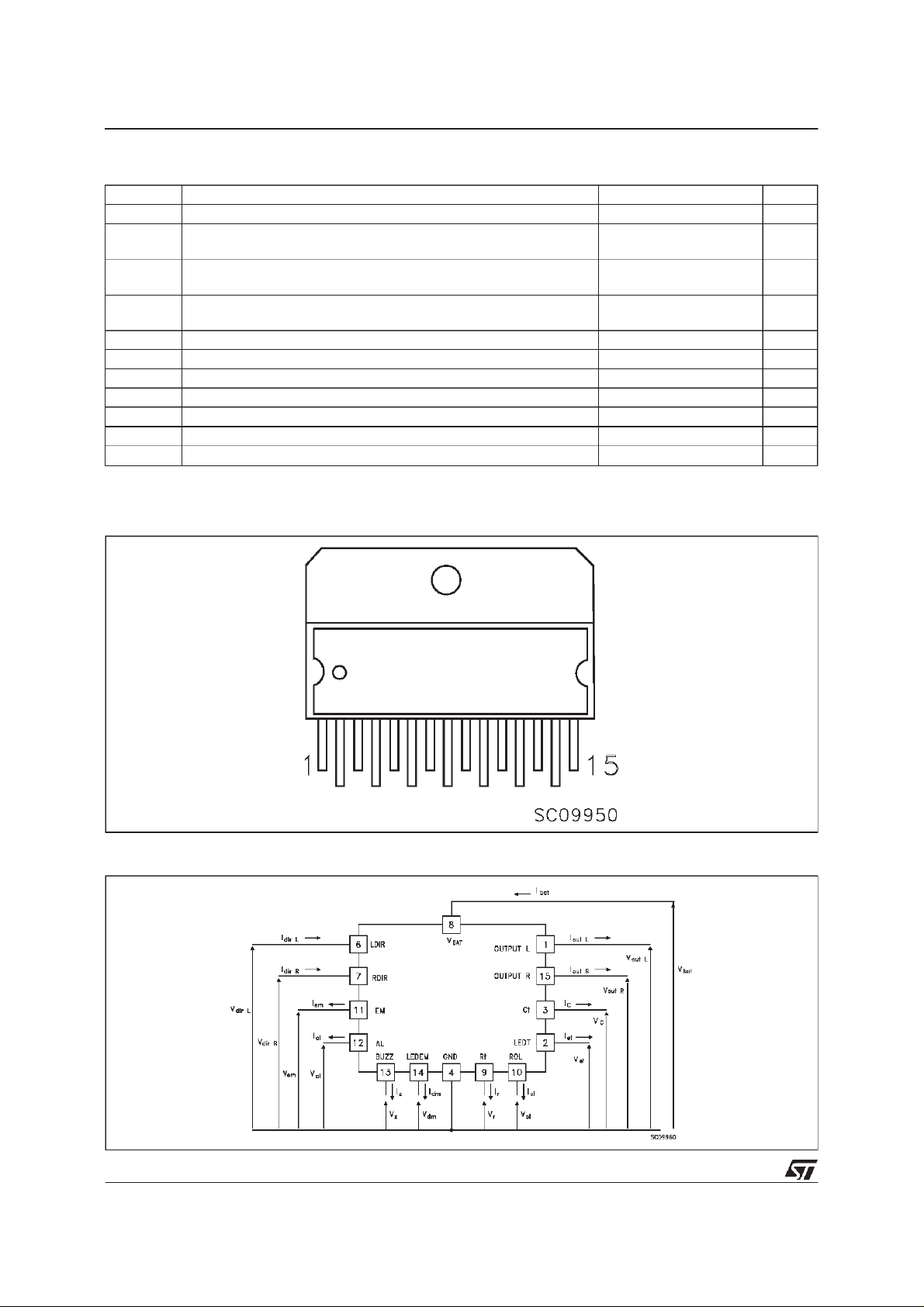
BLOCK DIAGRAM
March 1998
1/11
Page 2
VN410
ABSOLUTEMAXIMUMRATING
Symb o l Para met er Val u e Uni t
-Vbat Reverse Supply Voltage -12 V
V
BR(DSS)
V
I
I
Out
V
I
V
P
T
T
Note 1: In case the voltage drops beetween ground connection exceed 0.4V, extenal resistors in series with EM pin and AL pin areneeded
(if these pins are used)to prevent damages to the device. The value of these resistors is 100Ω.
CONNECTIONDIAGRAM
Drain-S o ur ce B reakdown V olt ag e 60
(Internally clamped)
Break dow n Voltage in Pad : LE DE M (V
p1
Break dow n Curre nt in Pad : RT , CT , R O L
p1
LDIR,RDI R
(V
bat
bat
<15V)
> 15V )
V
bat
15
+/- 10
-10/+100
Maximum DC Load Curr ent 15 A
Volt age Drop Bet we en grou nd co nnec tions (see note 1) 0.4 V
gnd
Reverse Ou tput Current -15 A
R
Electrostatic Discharge (R = 1.5 kΩ, C = 100 pF ) 2000 V
esd
Power Dissipation at Tc≤ 25oC Int ernally Li mit ed W
tot
Junction Oper at in g Temper at ure Int ernally Li mit ed
j
St orage Temperature -55 t o 150
stg
V
V
V
mA
mA
o
C
o
C
CURRENT ANDVOLTAGECONVENTIONS
2/11
Page 3

ELECTRICALTRANSIENTS REQUIREMENTS
VN410
ISO T/ R
TEXT LEVEL S
7637/1
Test Pulse
I II II I IV Delays and
1 -25 V -50 V -75 V -100 V 2 ms , 10 Ω
2 +2 5 V +50 V +75 V +100 V 0.2 m s , 10 Ω
3a -25 V -50 V -100 V -150 V 100 µs, 50 Ω
3b +25 V +5 0 V +75 V +100 V 100 µs, 50 Ω
4 -4 V -5 V -6 V -7 V 100 ms , 0. 0 1 Ω
5 +26.5 + 46.5 + 6 6. 5 +86.5 400 ms, 2 Ω
ISO T/ R
TEXT LEVELS RESULTS ∗
7637/1
Test Pulse
I II III IV
1C C E E
2C C E E
3a C C C C
3b C C C C
4C C C C
5C C E E
* :with an external capacitor of 22nF connected between V
10µH output inductance.
and GND, with loads connected(2 bulbs per channel),and with a maximum of
bat
CLAS S CONTENTS
Impedance
C All f unction of the dev ic e ar e per f ormed as designed af t e r expos ure to disturbance.
E O ne or more fu nc tions of the de vice i s not perf or med as desig ned aft er exposure and
cannot be returned to pr op er operat ion without r eplacing the devic e.
3/11
Page 4

VN410
THERMALDATA
R
thj-case
ELECTRICAL CHARACTERISTICS (10V < VCC<18V;-40oC<TJ< 125oC unlessotherwise
specified)
POWER
Symbol Parameter Test C ondition s Min. Typ. Max. Un it
V
R
I
SWITCHING
Symbol Parameter Test C ondition s Min. Typ. Max. Un it
(di/dt)
(di/dt)
Thermal Resistance Junction-case (1) Max 1.5
Oper at i ng Voltage 6 13 18 V
bat
On State Resis t a nc e
on
(per C hannel )
Supply Quies c ent
sq
Current
Tur n-on Current Slope R
on
Tur n-of f C urr ent Slope R
off
TC=25oCV
I
out=Inominal
TC=25oCV
bat
bat
=13V
=13V
Off State
=2.7Ω; TC=25oC; V
load
=2.7Ω; TC=25oC; V
load
=13 V 0.01 A /µ s
bat
=13 V 0.01 A /µ s
bat
0.07 Ω
100 µA
o
C/W
FLASHING
Symbol Parameter Test C ondition s Min. Typ. Max. Un it
f
δ
δ
I
dir
I
dir
I
em
I
I
dm1
I
dm2
I
I
T
T
T
I
df1
I
df2
I
Flas hing frequen c y
b
Rt= 2400
Ω
Ct=100 nF 2 4 1.6 Hz
(normal operation)
Duty C y cle Directi on Indic ator Flashing M ode 0.45
1
Duty C y cle Emergency and Alarm F lashing
2
0.35
Mode
Direction Currents R
L
=470Ω;R2= 470 Ω ;TC=25oC5 2040mA
1
R
Emer gency S ourc e
Vem=1V; TC=25oC52040mA
Current
Alarm So urce Current Val=2V; TC=25oC52040mA
al
LED Sour c e Cur rent
LEDEM pin s hort circuited to GND 35 120 mA
(emer gen c y flashing)
LED Sink Curr ent
15 70 mA
(emer gen c y flashing)
LED Curr ent ( trailer
et
LEDT pin shor t c irc u it ed t o GND 35 120 mA
indicat o r)
Buzz e r Current BUZ Z pin short cir cuited to GND 250 1000 mA
z
On Time Buzzer Rt = 3000 Ω; Ct= 100 nF 348 ms
z
Buzzer Filter Time Rt = 3 000 Ω; Ct= 1 00 n F 8 28 ms
fz
Alarm F iltering Tim e Rt = 3000 Ω; Ct= 100 nF 15 40 m s
al
Current T hreshold f or
Rol= 1 000 Ω; V
= 10 V 1.94 3.04 A
bat
Double Frequ ency
Current T hreshold f or
Rol= 1 000 Ω; V
= 18 V 2.64 4.22 A
bat
Double Frequ ency
Current T hreshold f or
t1
Rol= 1 000 Ω; V
= 10 V 3.52 4.56 A
bat
Tr ailer Det ection
4/11
Page 5

VN410
ELECTRICAL CHARACTERISTICS (continued)
FLASHING
Symbol Parameter Test C ondition s Min. Typ. Max. Un it
I
PROTECTIONS
Symbol Parameter Test C ondition s Min. Typ. Max. Un it
V
T
T
V
V
Current T hres h old for
t2
Tr ailer Detection
Under V ol ta ge
usd
Shut -down
Ther mal Limitation
pl
Tem perature
Ther mal Limitation
pr
Reset T emperatu re
Over Voltage
ov
Shut -down
Drain-S o ur ce Clam p
cl
Volt age
Rol = 1000 W ; Vbat = 18 V 4.81 6.33 A
6V
140 200
125
18 24 V
Iout = In=4.8A 60 80 V
o
C
o
C
EXTERNAL COMPONENTSCHARACTERISTICS (ApplicationRatings)
Symb o l Para met er Mi n . Typ . Max. Unit
R
C
R
R
R
R
I
EXTERNALCOMPONENTS DIAGRAM
L
Ext er na l Res istor for O s c illat or 3000 Ω
t
Ext er na l Cap acit or for Os cillat or 100 nF
t
Ext er na l Dir ect ion R es istor 447 470 4 93 Ω
1
Ext er na l Dir ect ion R es istor 447 470 4 93 Ω
2
Swit ch Con t ac t R esis tor 0.1 10 Ω
C
Ext er na l Res istor for Dou ble Frequency and Tra iler
ol
857 866 8 75 Ω
Detections
Connect o r Leakag e Current Between Input Directi on Pins
lk
2mA
and Vbat Pin
Out put I n duc t a nc e 10 µHV
out
ig
5/11
Page 6

VN410
SWITCHINGPARAMETERSTEST CONDITIONS
TRUTH TABLE
Conditions Al Em Dir R Dir L OUT R OUT L
Normal Oper a ti on H
Ov er- voltage X X X X L L
Under-voltage X X X X L L
Power Ov erload In that case , t he duty cycle will be reduc ed s o as t o keep t he junct ion
Hiz= high i mpedance, L = low level, X= uns pecified, A =act ive, O =open, C=c l osed.
iz
H
iz
H
iz
H
iz
A
tem perat ure below T
Hiz
H
H
L
X
O
iz
iz
pl
O
C
X
X
O
C
O
X
X
L
L
A
A
A
L
A
L
A
A
FUNCTIONAL DESCRIPTION
- NORMALOPERATION
The righ t or lef t channel is act ivated by t he corr esponding p os i ti on of th e direction indica to r through the
direction input pins. Each time an o ut p ut ( or both) is a c tivated , th e buzzer is also activated t hrough t h e
BUZ Z pin at the double frequency t ha n the output(s). In emergenc y case, if t he emergency but t o n is
act ivated the two chan nels are t urned on. A t t he s ame t im e the emerge ncy red LED i s fl ashing . A n
anti- theft a larm can be connec te d to t he AL pin, in that con dition if t he ant i- t he f t alarm is used the t wo
channel s are activated.
- UNDER-VOLTAGEOR OVER-VOLTAGE CONDITION
In case the device detect s a n undervoltage or an ov e rv oltage c ondition the activat ed ch annel(s) ar e
automatica lly sw it c he d off whate ver the i nput com mands (LDI R, RDIR, AL, EM )
- TRAILER OPERATION
The tr a iler det e ct ion is achiev e d with the ROL ext ernal resistor. In that ca s e the green tr a iler LED is
flas hi ng through the pin LE DT in s ynchronis m with the ou t put s.
- LOW LOADCONDITION
The l ow load detect ion is a c hieved wit h th e ROL ex t er na l resisto r connected be tw een ROL pin and RT pin.
If a low load co ndi ti on has b een detecte d th e o ut p ut fl ashing fre quenc y o n the guilty channel and th e
buzzer frequency will be double ( in direction mode only) .
- POWER LIMITATIONCONDITION
In case of overloading of t he power out p ut s t he duty cyc le is reduc ed internally by the devic e it self so as t o
keep m aximum junction tem pe r ature w ithin safe l imit s.
- CHIP GROUND DISCONNECTION
If GN D pin is disconnected , the device will sw it ch of f prov ided V
does not exc eed 18 V.
bat
6/11
Page 7

FIGURE2: SwitchingWaveforms
VN410
7/11
Page 8

VN410
FIGURE3: Buzzer Functionality
TYPICALAPPLICATIONDIAGRAM
8/11
Page 9

MULTIWATT-15 MECHANICAL DATA
VN410
DIM.
A 5 0.197
B 2.65 0.104
C 1.6 0.063
D 1 0.039
E 0.49 0.55 0.019 0.022
F 0.66 0.75 0.026 0.030
G 1.02 1.27 1.52 0.040 0.050 0.060
G1 17.53 17.78 18.03 0.690 0.700 0.710
H1 19.6 0.772
H2 20.2 0.795
L 21.9 22.2 22.5 0.862 0.874 0.886
L1 21.7 22.1 22.5 0.854 0.870 0.886
L2 17.65 18.1 0.695 0.713
L3 17.25 17.5 17.75 0.679 0.689 0.699
L4 10.3 10.7 10.9 0.406 0.421 0.429
L7 2.65 2.9 0.104 0.114
M 4.25 4.55 4.85 0.167 0.179 0.191
M1 4.63 5.08 5.53 0.182 0.200 0.218
S 1.9 2.6 0.075 0.102
S1 1.9 2.6 0.075 0.102
Dia1 3.65 3.85 0.144 0.152
MIN. TYP. MAX. MIN. TYP. MAX.
mm inch
0016036
9/11
Page 10

VN410
MULTIWATT-15 (In-Line) MECHANICAL DATA
DIM.
MIN. TYP. MAX. MIN. TYP. MAX.
A 5 0.197
B 2.65 0.104
C 1.6 0.063
E 0.49 0.55 0.019 0.022
F 0.66 0.75 0.026 0.030
G 1.14 1.27 1.4 0 .045 0.050 0.055
G1 17.57 17.78 17.91 0.692 0.700 0.705
H1 19.6 0.772
H2 20.2 0.795
L 26.55 27.05 1.045 1.065
L1(*) 25.35 25.8 0.998 1.016
L3 17.25 17.5 17.75 0.679 0.689 0.699
L4 10.3 10.7 10.9 0.406 0.421 0.429
L7 2.65 2.9 0.104 0.114
S 1.9 2.6 0.075 0.102
S1 1.9 2.6 0.075 0.102
Dia1 3.65 3.85 0.144 0.152
mm inch
10/11
0016037
Page 11

VN410
Information furnished is believed to be accurate and reliable. However, SGS-THOMSON Microelectronics assumes no responsability for the
consequences of use of such information nor for any infringement of patents or other rights of third parties which may resultsfrom its use. No
license is granted by implication or otherwiseunder any patent orpatent rights of SGS-THOMSON Microelectronics. Specifications mentioned
in this publication are subjectto change without notice. This publication supersedes and replaces all information previously supplied.
SGS-THOMSON Microelectronicsproducts are notauthorized foruse as criticalcomponents in lifesupport devices orsystems without express
written approval of SGS-THOMSON Microelectonics.
1998 SGS-THOMSON Microelectronics - Printed in Italy - All Rights Reserved
Australia - Brazil - Canada - China - France - Germany - Italy - Japan - Korea - Malaysia - Malta - Morocco - The Netherlands -
Singapore - Spain - Sweden - Switzerland - Taiwan - Thailand - United Kingdom - U.S.A
SGS-THOMSON Microelectronics GROUP OF COMPANIES
...
11/11
 Loading...