

Page 1
VN380
TYPE V
VN38 0 60 V 5 A 0.11 Ω
VN380SP 60 V 5 A 0.11 Ω
■ LOADCURRENT UP TO 7 A
■ CMOS COMPATIBLE
■ THERMALSHUTDOWN
■ DIGNOSTICOUTPUT
■ INTEGRATEDCLAMPS
■ OVERCURRENT PROTECTION
■ OPENCOIL DETECTION
■ OVERVOLTAGEDECTION
load(c l)
I
n
R
on
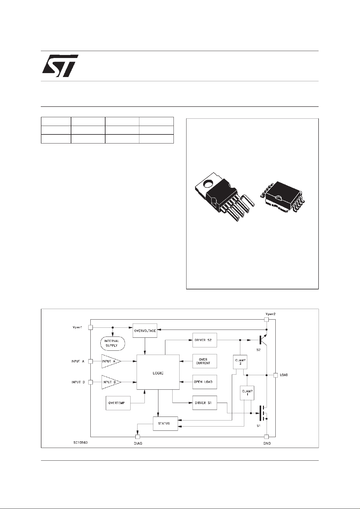
DESCRIPTION
The VN380 is a monolithic device made using
STM VIPower Technology, intended for driving
inductive loads. The inputs are CMOS
compatible. The diagnostic output provides an
indication of open load and demagnetization
mode. Built-in thermal shut-down protects the
chip from over-temperature. In case or
over-current or over-temperature or over-voltage
the product will automatically operate in
recirculationmode.
VN380SP
SMART SOLENOID DRIVER
SOLID STATE RELAY
10
1
HEPTAWATT PowerSO-1O
ORDER CODES:
HEPTAWATT VN380
PowerSO-1O VN380SP
BLOCK DIAGRAM
June 1998
1/9
Page 2
VN380
ABSOLUTEMAXIMUMRATING
Symb o l Para met er Val u e Uni t
V
load
I
load
I
rload
E
E
I
I
diag
V
V
pwr1
V
pwr2
RV
T
T
V
V
diag
C
load
Note (❉) :Higher temperatureis allowed during a short time
before thermal shutdown. Permanent operation above
not allowed.
Maximum DC Load V ol t age (Internally c la m ped) V
Maximum DC Load Cur rent (Internally clamped) A
Revers e Load Current , T
Maximum Clam ping Energy , T
c
= 25oC-10A
case
= 150oC, f = 40 Hz,
case
100 mJ
1000 hou rs (f : Input A fr e quenc y)
Maximum Clam ping Energy , T
c
= -40oC,f=75Hz,
case
200 mJ
5 m inut es (f : I nput A fr eque nc y)
Input s C urr ent +/- 10 mA
in
Diagnostic O ut put Current +/- 10 mA
Electrostatic Discharge (R = 1.5 kΩ, C = 100 pF, all pins) 2000 V
esd
Power Voltage 1 60 V
Power Voltage 2 60 V
Reverse Power Voltage -0.3 V
pwr
Junction Operat ing Tempe rat ure -40 to 150 (❉)
j
St orage Tem per at ure -55 t o 150
stg
Input Volt ages 8 V
in
Diagnostic O ut put Voltag e 8 V
Load Cap acit y 1 µF
o
C 150is
o
C
o
C
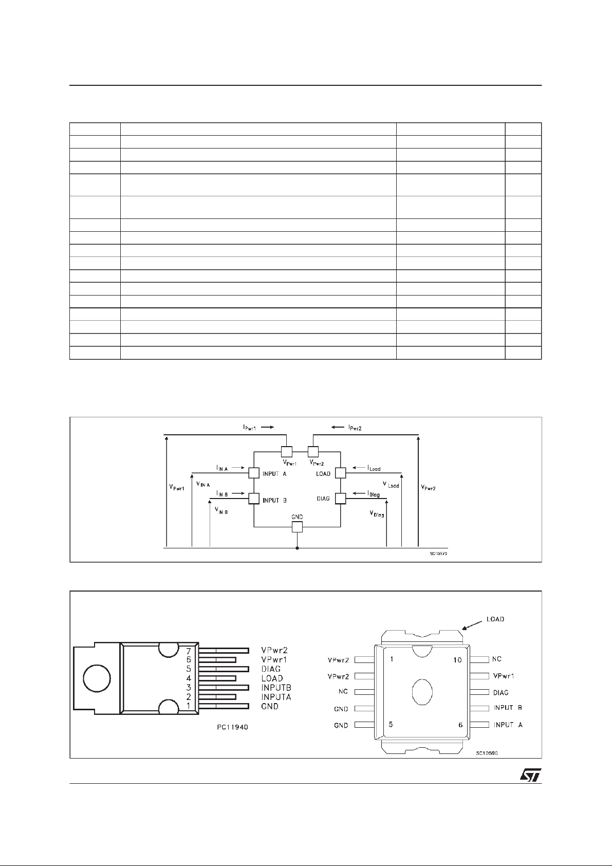
CURRENT ANDVOLTAGE CONVENTIONS
CONNECTION DIAGRAM
HEPTAWATT PowerSO-10
2/9
Page 3

THERMALDATA
R
thj-case
R
thj-amb
(∗) When mounted using minimum recommended pad size on FR-4 board.
Ther mal Resist ance Junct ion-c ase Max 1.8 1.67
Ther mal Resist ance Junct ion-am b ient (∗) Max 60 50
HEPTAWATT PowerSO-10
VN380
o
C/W
o
C/W
ELECTRICAL CHARACTERISTICS (10V < V
<18V;- 40oC<TJ< 150oC unless otherwise
PWR1
specified)
POWER
Symbol Parameter Test Conditions Min. Typ. Max. Unit
V
R
R
V
ce(sat)
pwr1
I
Oper at i ng V o lt age 6 13 24 V
On S t ate Resist ance
on1
(exc it a t ion pat h )
On S t ate Resist ance
on2
(reci rc ula t ion path)
Saturation Voltage of
Bipolar S2
Supply Quiesc ent
sq
I
load=In
V
inA=VinB
V
pwr1
V
inA
=5A
=5V
=13V I
=5V V
load=In
Iload = In=5A
V
pwr1=Vpwr2
I
=10A TJ>125oC
load
V
pwr1=Vpwr2
V
=13V V
pwr1
=13V
=13V
=GND
inB
inA=VinB
=5A
=5V 25 mA
0.2 Ω
0.4 Ω
2
2
Current
I
Out put Le ak age
lk
V
=18V V
pwr1
inA=VinB
=GND 5 mA
Current
I
Off State Supply
off
Current
V
inA=VinB
V
= Not Conn ected
pwr1
10V<V
T
=25oC
J
pwr2
=GND
<24V
50 µA
SWITCHING(EXCITATION PATH)
V
V
Symbol Parameter Test Conditions Min. Typ. Max. Unit
t
d(on)
Turn-on D elay Time R
t
Rise Time o f Output
r
load
R
load
=2.5Ω V
=2.5
Ω
= 5 V (see fig.1) 50 µs
inA
V
= 5 V (see fig.1 ) 1 20 µs
inA
Current
t
d(off)
Turn-off Delay T ime R
t
Fall Time of O ut put
f
load
R
load
=2.5
Ω
=2.5Ω V
V
= 5 V (see fig.1 ) 50 µs
inA
= 5 V (see fig.1) 1 20 µs
inA
Current
LOGIC INPUT
Symbol Parameter Test Conditions Min. Typ. Max. Unit
V
V
i(hyst)
V
V
i(CL)
I
Input Low Level
il
Volt age
Input Hig h Lev el
ih
3.5 V
Volt age
Input hysteresis
0.5 0.8 2 V
Volt age
Input Cla m p Volt ag e Iin = 10 m A 8 9.5 11 V
Input Current VinA = V
in
V
inA=VinB
inB
=2V
=5V
20
1.5 V
250
µA
µA
3/9
Page 4

VN380
ELECTRICAL CHARACTERISTICS (continued)
PROTECTIONS AND DIAGNOSTICS
Symbol Parameter Test Conditions Min. Typ. Max. Unit
T
I
lim
V
V
diag
V
diag(CL)
T
Ther mal Shut-D own
tsd
160 180 200
Tem perature
Current Cut O f f Level 15 30 A
Ov er Volt age Th res ho ld Vi nA = V
ov
=5V 27 V
inB
St at us O ut put Volt a ge Di agnos tic O ut p ut Act ive (low)
Idiag = 2 mA
St at us O ut put Clamp
Idiag = 1 0 mA 8 9.5 11 V
Volt age
St at us P ropaga t ion
d
Delay
Demagnetizati on Mode
(F ast tu rn- off)
Vdiag = 1 V (see figu re 3) 70 µ s
0.5 V
o
C
V
Switch S1 Detecti on
cl1
Iload = In=5A 607080 V
Clamp
V
cl2
Out put I n duct ive
Iload = In= 5 A 24 28.5 33 V
Clamp Voltage
V
Fly back D iagnostic
fb
Threshold
I
Oper Load Cur r ent
ol
Demagnetizati on Mode
(F ast tu rn- off)
Vcl = V
cl1orVcl2
Vcl -5 V
cl
5700mA
Level
TRUTH TABLE
Conditions IN A I N B S1 S2
Sta ndb y Mod es L
L
Excitation Mode H H ON OFF
Recirculation Mo de H L OFF ON
Demagne t iz ation Mode
(Fast turn off)
V
pwr2+Vcl2<Vcl1
V
pwr2+Vcl2>Vcl1
L
L
Thermal Shutdown H H OFF ON
Current Cut O f f H H OFF ON
Open Load See Ope n Lo ad W av e f orm s
Ov erv o lt age H H OF F ON
L
H
L
L
OFF
OFF
OFF
ON
OFF
OFF
ON
OFF
V
4/9
Page 5

VN380
FUNCTIONAL DESCRIPTION
- CURRENT CUT OFF
When the load current rise above the current cut off level, S1 is automatically switched off and the
devicesoperates inrecirculationmode (S2 active).S1is latched off until Agoes low and highagain.
This default is not displayed by diagnostic flag.
- OPENLOAD
If the load current is below the open load current level, the flag of the open load block is activated but
this default is displayed by the diagnosticoutput on the fallingedge of input B and the diagnosticoutput
is latched at low level untilinput A goes low and high again. In case an open load is detected during an
active phase of input B, but disappears before a falling edge of input B, this default is not dispayed by
the diagnosticflag (see openload waveforms).
- THERMAL SHUTDOWN
The device is internally protected against over temperaturesby the thermal circuit protection. When the
device junction temperature exceeds the protection limit, S1 is automaticallyswitched off. Therefore the
device operates in recirculation mode (S2 active). S1 remain latched off until V
again. This default is not dispayed by the diagnostic flag.
OVERVOLTAGE
During the ON state of S1 switch, if V
pwr1
or V
is rising above the threshold detection S1 is
pwr2
automaticallyswitchedoff, thereforethe deviceoperatesin recirculationmode.
goes low and high
pwr1
FIGURE1: SWITCHINGPARAMETER TEST CONDITIONS
5/9
Page 6

VN380
FIGURE2: SwitchingWaveforms
FIGURE3
6/9
Page 7

HEPTAWATT (VERTICAL) MECHANICAL DATA
VN380
DIM.
A 4.8 0.189
C 1.37 0.054
D 2.4 2.8 0.094 0.110
D1 1.2 1.35 0.047 0.053
E 0.35 0.55 0.014 0.022
F 0.6 0.8 0.024 0.031
F1 0.9 0.035
G 2.41 2.54 2.67 0.095 0.100 0.105
G1 4.91 5.08 5.21 0.193 0.200 0.205
G2 7.49 7.62 7.8 0.295 0.300 0.307
H2 10.4 0.409
H3 10.05 10.4 0.396 0.409
L 16.97 0.668
L1 14.92 0.587
L2 21.54 0.848
L3 22.62 0.891
L5 2.6 3 0.102 0.118
L6 15.1 15.8 0.594 0.622
L7 6 6.6 0.236 0.260
M 2.8 0.110
M1 5.08 0.200
Dia 3.65 3.85 0.144 0.152
MIN. TYP. MAX. MIN. TYP. MAX.
mm inch
P023A
7/9
Page 8

VN380
PowerSO-10MECHANICAL DATA
DIM.
mm inch
MIN. TYP. MAX. MIN. TYP. MAX.
A 3.35 3.65 0.132 0.144
A1 0.00 0.10 0.000 0.004
B 0.40 0.60 0.016 0.024
c 0.35 0.55 0.013 0.022
D 9.40 9.60 0.370 0.378
D1 7.40 7.60 0.291 0.300
E 9.30 9.50 0.366 0.374
E1 7.20 7.40 0.283 0.291
E2 7.20 7.60 0.283 0.300
E3 6.10 6.35 0.240 0.250
E4 5.90 6.10 0.232 0.240
e 1.27 0.050
F 1.25 1.35 0.049 0.053
H 13.80 14.40 0.543 0.567
h 0.50 0.002
L 1.20 1.80 0.047 0.071
q 1.70 0.067
α 0
o
o
8
==
==
HE
h
A
F
A1
610
51
eB
M
0.25
D
==
D1
==
DETAIL”A”
E2
==
DETAIL”A”
Q
B
0.10 A
E1E3
==
SEATING
PLANE
A
C
α
B
E4
==
SEATING
PLANE
A1
L
==
0068039-C
8/9
Page 9

VN380
Information furnished is believed tobe accurate and reliable. However, STMicroelectronics assumes no responsibility for theconsequences
of use of such information nor for any infringement of patents or other rights of third parties which may result from its use. No license is
granted by implication or otherwise under any patent or patent rights of STMicroelectronics. Specification mentioned in this publication are
subject to change without notice. This publication supersedes and replaces all information previously supplied. STMicroelectronics products
are not authorized for use as critical components in life support devices or systems without express written approval of STMicroelectronics.
Australia - Brazil - Canada - China - France- Germany- Italy- Japan - Korea - Malaysia -Malta - Mexico - Morocco- TheNetherlands -
Singapore - Spain - Sweden- Switzerland - Taiwan- Thailand - United Kingdom- U.S.A.
The ST logois a trademark of STMicroelectronics
1998 STMicroelectronics – Printed in Italy – All RightsReserved
STMicroelectronics GROUP OFCOMPANIES
.
9/9
 Loading...