

Page 1
PRELIMINARY DATA SHEET
Bi-CMOS INTEGRATED CIRCUIT
µ
PC2539
RDS DATA DEMODULATOR IC
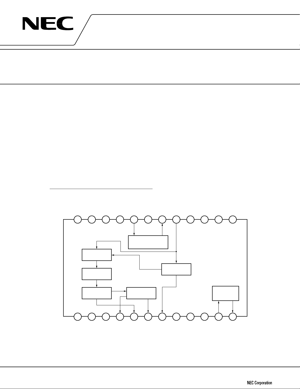
The µPC2539 is data demodulator IC for FM receiver applying to Radio Data System in European countries and
Radio Broadcasting Data System in USA.
This IC carries out to extract 57kHz RDS signal from FM multiplex signal, demodulate data-stream, recover
bit-rate-clock, and discriminate SK signal in ARI system.
FEATURES
• Adjustment-free
• Built-in 57kHz band-pass-filter consist of switched capactiors.
• High sensitivity.
• Employing digital PLL.
• Small outline plastic package
ORDERING INFORMATION
Part Number Package
µ
PC2539GS 24-pin plastic SOP (300 mil)
BLOCK DIAGRAM
24 23 22 21 20 19 18 17 16 15 14 13
COSTAS
BIPHASE
DECODER
DIFFERENTIAL
DECODER
123456789101112
57kHz BPF
CLOCK
RECOVERY
SK DET
OSC
The information in this document is subject to change without notice.
Document No. S11570EJ1V0DS00 (1st edition)
Date Published May 1996 P
Printed in Japan
©
1996
Page 2
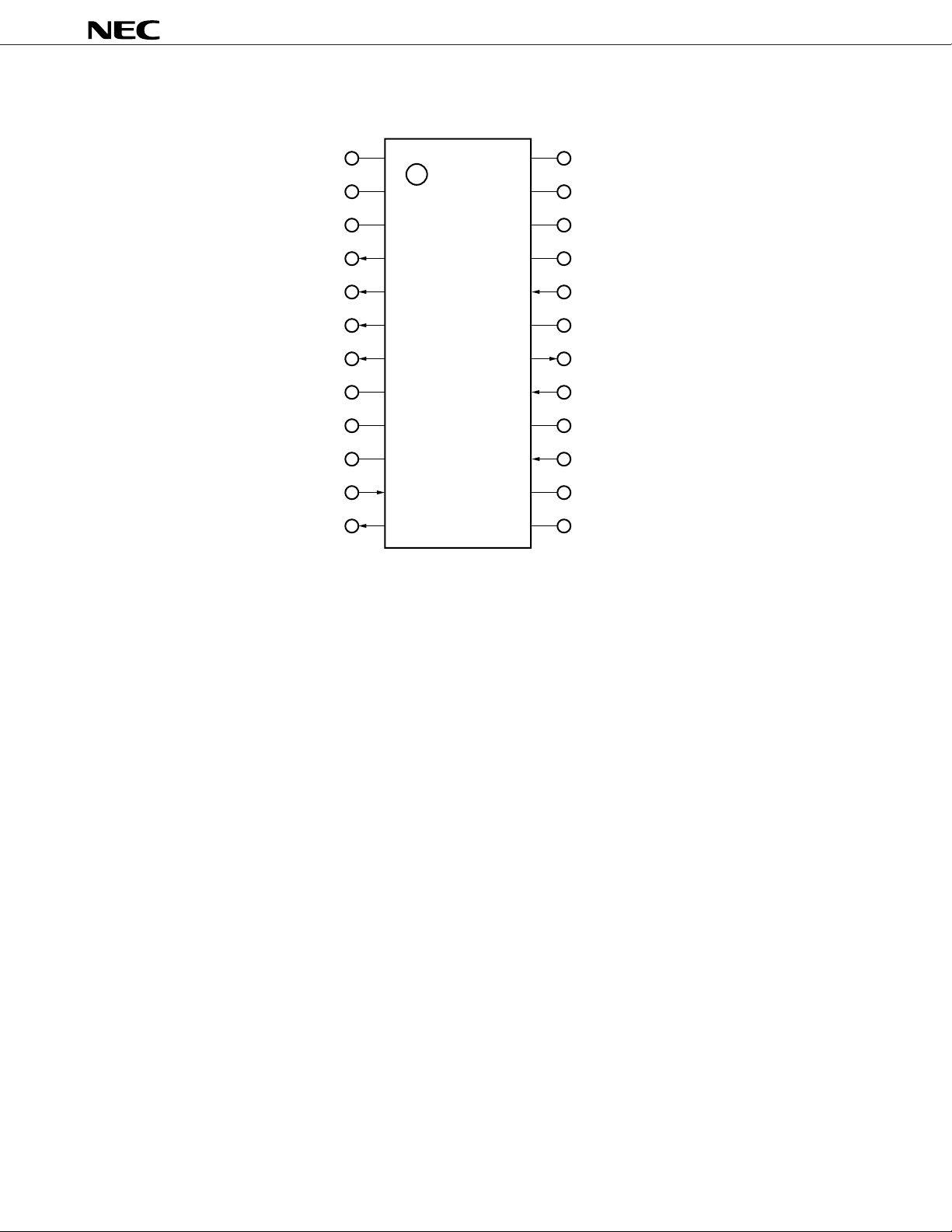
PIN CONFIGURATION (Top View)
V
µ
PC2539
DD
1
24
CC
V
TEST1
TEST2
CLK OUT
DATA OUT
RDS IND
SK IND
TEST3
TEST4
DGND
OSC IN
OSC OUT
10
11
12
2
3
4
5
6
7
8
9
23
22
21
20
19
18
17
16
15
14
13
TEST9
TEST8
TEST7
BPF IN
REF
BPF OUT
DSB IN
AGND
OP. CTL
TEST6
TEST5
2
Page 3
µ
PC2539
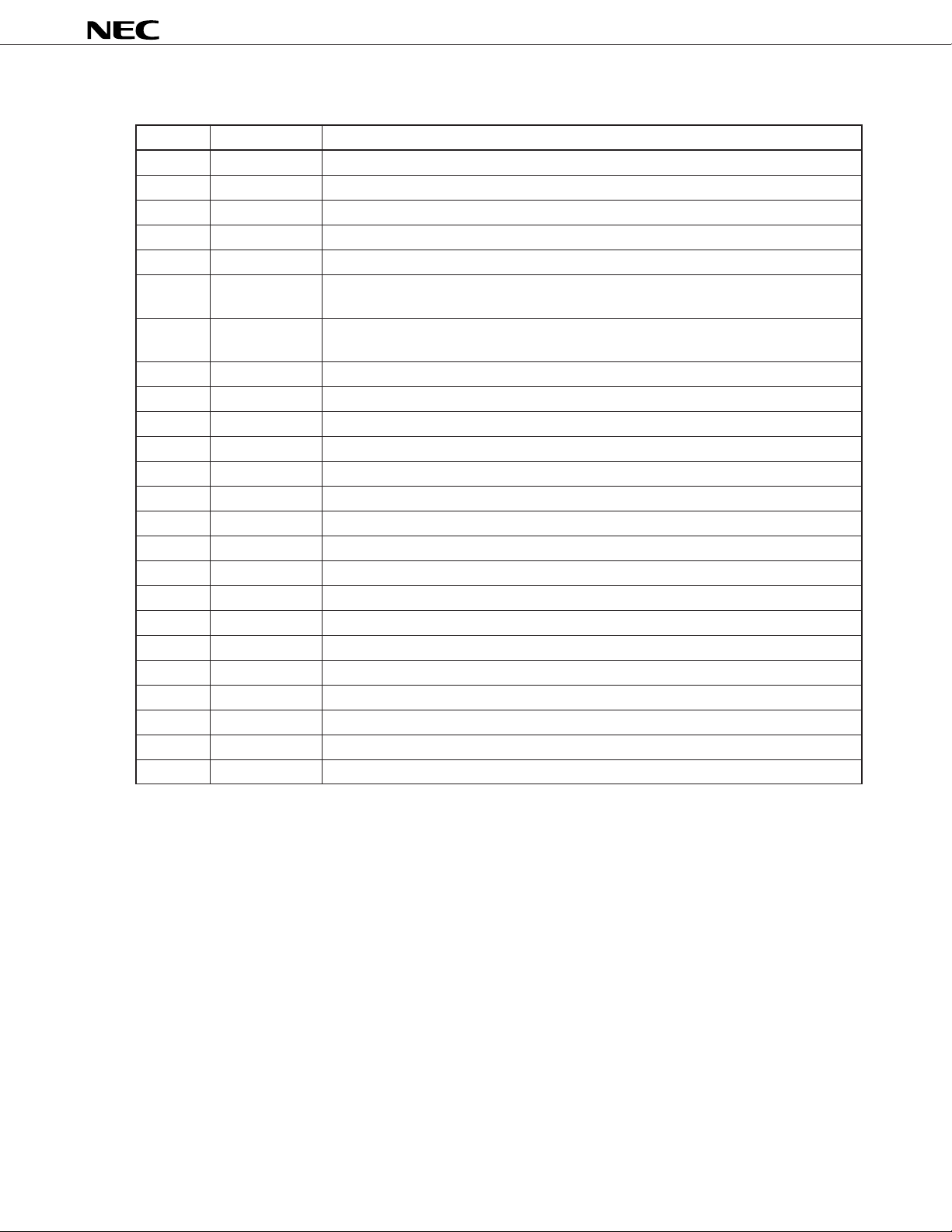
PIN FUNCTIONS
Pin no. Pin name Function
1VDD Power Supply for Digital Circuit
2 TEST1 Pin for Test : Normally connect to GND.
3 TEST2 Pin for Test : Normally be open.
4 CLK OUT Bit-Rate-Clock Output Pin
5 DATA OUT RDS Data Output Pin
6 RDS IND RDS Idenrification Indicator : When RDS signal is detected, the output voltage becomes
to Low level.
7 SK IND SK Identification Indicator : When SK signal is detected, the output voltage becomes to
Low level.
8 TEST3 Pin for Test : Normally connect to GND.
9 TEST4 Pin for Test : Normally connect to GND.
10 DGND GND for Digital Circuit
11 OSC IN Oscillator Input Pin
12 OSC OUT Oscillator Output Pin
13 TEST5 Pin for Test : Normally be open.
14 TEST6 Pin for Test : Normally connect to GND.
15 OP.CTL Operation/Stop control Pin : High:Operation mode, Low:Stop mode
16 AGND GND for Analog Circuit
17 DSB IN DSB Demodulator Input Pin
18 BPF OUT Band-Pass-Filter Output Pin
19 REF Reference Voltage for BPF
20 BPF IN Band-Pass-Filter Input Pin
21 TEST7 Pin for Test : Normally connect to GND.
22 TEST8 Pin for Test : Normally connect to GND.
23 TEST9 Pin for Test : Normally connect to GND.
24 VCC Power Supply for Analog Circuit
3
Page 4

µ
ELECTRICAL SPECIFICATIONS (PRELIMINARY)
ABSOLUTE MAXIMUM RATINGS (Unless otherwise specified, TA=25°C)
Parameter Symbol Conditions Ratings Unit
Supply voltage VCC VCC pin, VDD pin 7.0 V
Power dissipation Pd TA=85°C 280 mW
Operating ambient temperature Topt –30 to +85 °C
Storage temperature Tstg –40 to +125 °C
Caution Exposure to Absolute Macimum Rating for extended periods may affect device reliability;
exceeding the ratings could cause permanent damage. The parameters apply independently.
RECOMMENDED OPERATING CONDITIONS
Parameter Symbol Conditions MIN. TYP. MAX. Unit
Sypply voltage V CC VCC pin, VDD pin 4.5 5.0 5.5 V
FM Demoulation Signal Vin MONO, ∆f=75kHz 280 mVrms
Input Voltage
PC2539
ELECTRICAL CHARACTERISTICS (Unliss otherwise specified, TA=25°C, VCC=VDD=5.0V)
Parameter Symbol Conditions MIN. TYP. MAX. Unit
Circuit current ICC No Signal 10 15 20 mA
SK Detection Sensitivity(ON) Ssk1 SK ONLY 2.5 3.5 4.5 mVrms
SK Detection Sensitivity(OFF) Ssk2 SK ONLY 1.0 2.0 3.0 mVrms
RDS Detection Sensitivity Srds RDS ONLY, DATA(101010..) 0.1 0.2 0.6 mVrms
SK Lock Up Time Tsk SK ONLY, Vsk=10mVrms 12 16 20 bit
RDS Lock Up Time 1 Trds1 RDS ONLY 10 40 80 bit
RDS Lock Up Time 2 Trds2 RDS+SK, Vsk=10mVrms 20 50 100 bit
Output Voltage(H Level) VOH Io=±100µA, Pin 4, 5, 6 4.90 4.95 – V
Io=±5µA, Pin 7 4.90 4.95 – V
Output Voltage(L Level) VOL Io=±100µA, Pin 4, 5, 6 – 0.05 0.10 V
Io=±5µA, Pin 7 – 0.05 0.10 V
Band-Pass-Filter Characteristics
Peak Gain Av fin=57kHz, Vin=10mVrms 22 25 28 dB
Pass Band Width BW Av-3dB 2.8 3.3 3.8 kHz
Attenuation 1 ATT1 fin=53kHz, Vin=10mVrms 23 27 31 dB
Attenuation 2 ATT2 fin=38kHz, Vin=10mVrms 75 85 – dB
Maximum Input Level Vinmax fin=57kHz 120 150 – mVp-p
Signal to Noise Ratio S/N fin=57kHz, Vin=3mVrms 25 30 – dB
Input Impedance Zin 26 35 44 kΩ
Output Impedance Zout – 300 660 Ω
4
Page 5

TIMING CHART OF DATA OUTPUT AND CLOCK OUTPUT
µ
µ
µ
DATA OUTPUT
(From pin5)
CLOCK OUTPUT
(From pin4)
µ
PC2539
210.5
µ
s
±10 s
421.5
µ
s
±10 s
210.5
µ
s
±10 s
5
Page 6

APPLICATION CIRCUIT ESAMPLE
VCC=+5V
µ
0.1 F
µ
0.1 F
µ
100 F
+
24 23 22 21 20 19 18 17 16 15 14 13
COSTAS
INPUT
4700pF
0.1 F
57kHz BPF
µ
4700pF
+5V
OPERATE
STOP
µ
PC2539
BIPHASE
DECODER
DIFFERENTIAL
DECODER
123456789101112
µ
0.1 F
RECOVERY
DATA OUT
CLK OUT
CLOCK
RDS IND
SK DET
SK IND
+5V
RDS
RBDS
*1
OSC
4.332MHz
*2
22pF 22pF
Notes 1. Pin 7 does not have ability enough to drive LED directly because of internal serial resistor (10kΩ) shown
in following figure. In application for system with no ARI signal such as RBDS in USA, pin 7 is
recommended to be connected with VDD.
2. Crystal oscillation frequency tolerance : ± 100ppm
The equivalent circuit in pin 7
S K detector block
10k Ω
7
PLL block
6
Page 7

PACKAGE DRAWING
24 PIN PLASTIC SOP (300 mil)
112
G
µ
PC2539
1324
detail of lead end
P
A
H
I
J
F
E
C
D
NOTE
Each lead centerline is located within 0.12 mm (0.005 inch) of
its true position (T.P.) at maximum material condition.
M
N
M
K
B
L
ITEM MILLIMETERS INCHES
A
15.54 MAX.
B
0.78 MAX.
C
1.27 (T.P.)
D 0.40 0.016
E
F
G
H
I
J
K 0.20
L 0.6±0.2 0.024
M
N
P3° 3°
+0.10
–0.05
0.1±0.1
1.8 MAX.
1.55
7.7±0.3
5.6
1.1
+0.10
–0.05
0.12
0.10
+7°
–3°
0.612 MAX.
0.031 MAX.
0.050 (T.P.)
+0.004
–0.003
0.004±0.004
0.071 MAX.
0.061
0.303±0.012
0.220
0.043
+0.004
0.008
–0.002
+0.008
–0.009
0.005
0.004
+7°
–3°
P24GM-50-300B-4
7
Page 8

µ
PC2539
The application circuits and their parameters are for references only and are not intended for use in actual design-in's.
No part of this document may be copied or reproduced in any form or by any means without the prior written
consent of NEC Corporation. NEC Corporation assumes no responsibility for any errors which may appear in this
document.
NEC Corporation does not assume any liability for infringement of patents, copyrights or other intellectual
property rights of third parties by or arising from use of a device described herein or any other liability arising
from use of such device. No license, either express, implied or otherwise, is granted under any patents,
copyrights or other intellectual property rights of NEC Corporation or others.
While NEC Corporation has been making continuous effort to enhance the reliability of its semiconductor devices,
the possibility of defects cannot be eliminated entirely. To minimize risks of damage or injury to persons or
property arising from a defect in an NEC semiconductor device, customer must incorporate sufficient safety
measures in its design, such as redundancy, fire-containment, and anti-failure features.
NEC devices are classified into the following three quality grades:
“Standard“, “Special“, and “Specific“. The Specific quality grade applies only to devices developed based on
a customer designated “quality assurance program“ for a specific application. The recommended applications
of a device depend on its quality grade, as indicated below. Customers must check the quality grade of each
device before using it in a particular application.
Standard: Computers, office equipment, communications equipment, test and measurement equipment,
audio and visual equipment, home electronic appliances, machine tools, personal electronic
equipment and industrial robots
Special: Transportation equipment (automobiles, trains, ships, etc.), traffic control systems, anti-disaster
systems, anti-crime systems, safety equipment and medical equipment (not specifically designed
for life support)
Specific: Aircrafts, aerospace equipment, submersible repeaters, nuclear reactor control systems, life
support systems or medical equipment for life support, etc.
The quality grade of NEC devices in “Standard“ unless otherwise specified in NEC's Data Sheets or Data Books.
If customers intend to use NEC devices for applications other than those specified for Standard quality grade,
they should contact NEC Sales Representative in advance.
Anti-radioactive design is not implemented in this product.
M4 94.11
8
 Loading...