

Page 1
DATA SHEET
DATA SHEET
BIPOLAR ANALOG INTEGRATED CIRCUIT
PC24A00 Series
µ
THREE TERMINAL LOW DROPOUT VOLTAGE REGULATOR
The µPC24A00 Series is a low dropout voltage three terminal regulator that has realized a minimum voltage
differential between the I/O of no more than 1 V when the output current is 2 A through the employment of a PNP
transistor at the output stage.
Due to its ability to achieve a greater reduction in the power loss compared with conventional three-terminal
regulators, the µPC24A00 Series is ideal for use as the secondary side smoothing circuit of a power supply.
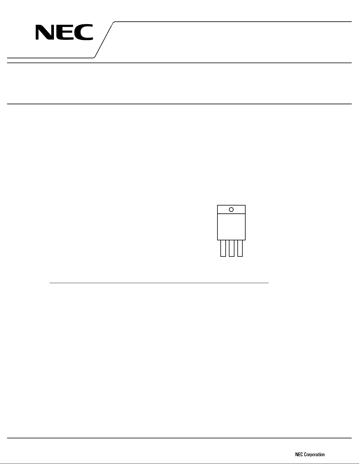
FEATURES PIN CONFIGURATION (Marking Side)
Output current in excess of 2.0 A
•
High accuracy of output voltage
•
∆VO = ±2% MAX. (TJ = 25°C, IO = 1 A)
Low dropout voltage
•
DIF
V
= 1 V MAX. (IO = 2 A)
On-chip thermal shut down circuit, over-current protection
•
circuit and safe operating area protection circuit
3-pin plastic SIP (MP-45G)
µPC24A05HF, 24A12HF, 24A15HF
3
12
ORDERING INFORMATION
Part Number Package Output Voltage
PC24A05HF 3-pin plastic SIP (MP-45G) (isolated TO-220) 5 V
µ
PC24A12HF 3-pin plastic SIP (MP-45G) (isolated TO-220) 12 V
µ
PC24A15HF 3-pin plastic SIP (MP-45G) (isolated TO-220) 15 V
µ
1: INPUT
2: GND
3: OUTPUT
The information in this document is subject to change without notice. Before using this document, please
confirm that this is the latest version.
Not all devices/types available in every country. Please check with local NEC representative for
availability and additional information.
Document No. G14632EJ3V0DS00 (3rd edition)
Date Published February 2000 N CP(K)
Printed in Japan
©
2000
Page 2
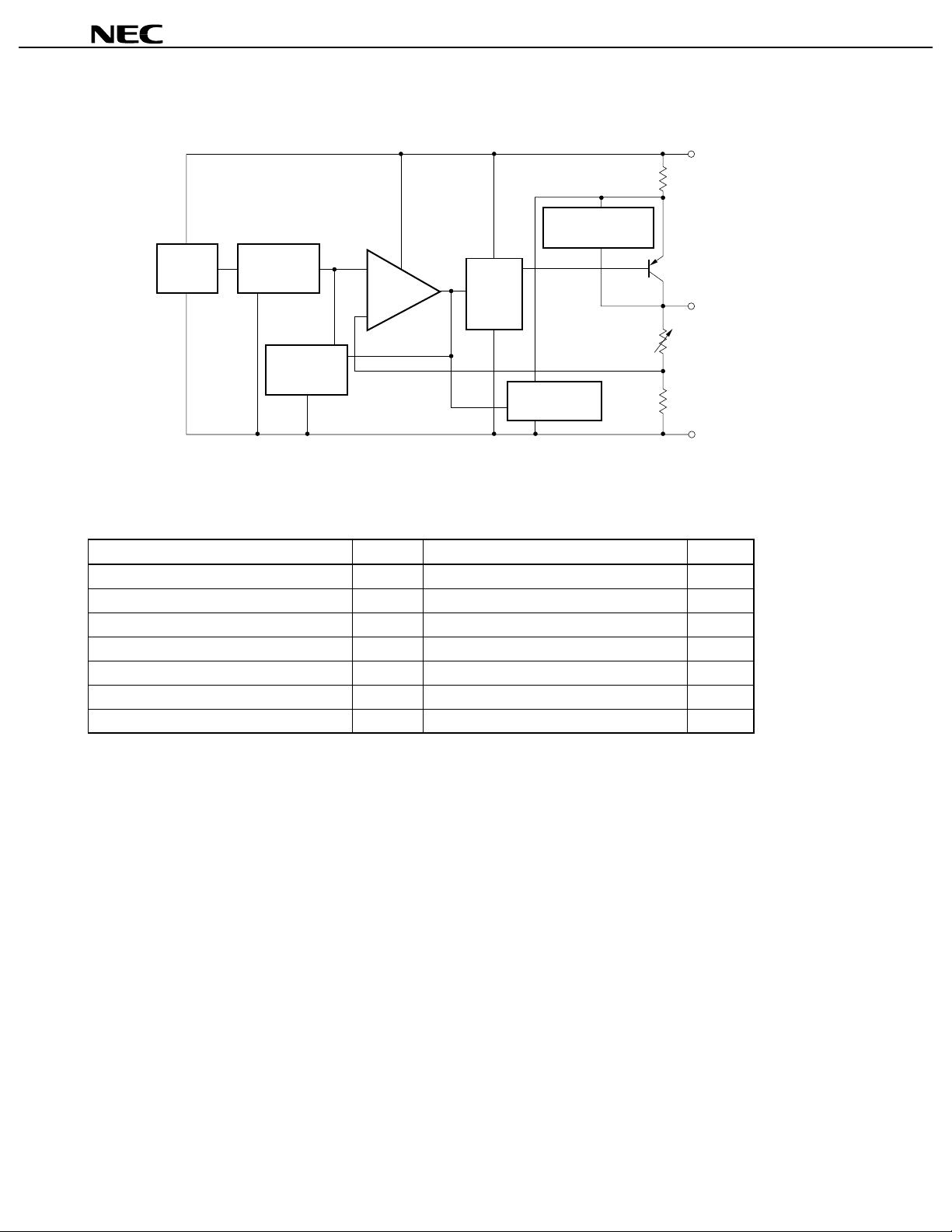
BLOCK DIAGRAM
Start-up
circuit
Reference
voltage
Thermal
shut down
Error
amp.
Drive
circuit
Safe operating
area protection
Over-current
protection
µµµµ
PC24A00 Series
INPUT
OUTPUT
GND
A
= 25
ABSOLUTE MAXIMUM RATINGS (T
Parameter Symbol Rating Unit
Input voltage V
Total power consumption P
Operating ambient temperature T
Storage temperature T
Operating junction temperature T
Thermal resistance (junction to case) R
Thermal resistance (junction to ambient) R
Internally limited. When operating junction temperature rise up to 150°C, the internal circuit shutdown output
Note
C, Unless Otherwise Specified)
°°°°
IN
T
A
stg
J
th (J−C)
th (J−A)
0.3 to +36 V
−
Note
20
20 to +85
−
55 to +150
−
20 to +150
−
5
65
C/W
°
C/W
°
W
C
°
C
°
C
°
voltage.
Caution Product quality may suffer if the absolute maximum rating is exceeded even momentarily for any
parameter. That is, the absolute maximum ratings are rated values at which the product is on the
verge of suffering physical damage, and therefore the product must be used under conditions that
ensure that the absolute maximum ratings are not exceeded.
2
Data Sheet G14632EJ3V0DS00
Page 3
µµµµ
PC24A00 Series
TYPICAL CONNECTION
D1
PC24A00
INPUT
CIN
µ
+
COUT
CIN: 0.1 to 0.47 µF. Be sure to connect to prevent abnormal oscillation. When using capacitors, film capacitors with
excellent voltage and temperature characteristics are recommended. Be aware that some monolithic ceramic
capacitors have inferior temperature and voltage characteristics. When using a monolithic ceramic capacitor,
CIN requires a capacitor that can secure this capacity within the voltage and temperature range used.
OUT
C
: 10 µF or higher. Be sure to connect to prevent oscillation and to improve transient load stabilization.
OUTPUT
D2
Remark
Connect CIN and C
D1:VO > V
IN
required
OUT
as close as possible to the IC pins (within 2 cm).
D2: Shottky barrier diode required for when VO < GND.
RECOMMENDED OPERATING CONDITIONS
Parameter Symbol Condition MIN. TYP. MAX. Unit
Input voltage V
Output current I
Operating junction temperature T
Caution The recommended operating range may be exceeded without causing any problems provided that
the absolute maximum ratings are not exceeded. However, if the device is operated in a way that
exceeds the recommended operating conditions, the margin between the actual conditions of use
and the absolute maximum ratings is small, and therefore thorough evaluation is necessary. The
recommended operating conditions do not imply that the device can be used with all values at their
maximum values.
IN
O
J
PC24A05HF 6 9 15 V
µ
PC24A12HF 13 18 22 V
µ
PC24A15HF 16 22 25 V
µ
All 0 2 A
All
20
−
+
125
C
°
Data Sheet G14632EJ3V0DS00
3
Page 4
ELECTRICAL CHARACTERISTICS
µµµµ
PC24A00 Series
PC24A05 (TJ = 25
µµµµ
C, VIN = 9 V, IO = 1 A, Unless Otherwise Specified)
°°°°
Parameter Symbol Condition MIN. TYP. MAX. Unit
O
0
J
T
≤ 125°C,
°C ≤
IN
Line regulation REG
Load regulation REG
BIAS
Quiescent current change
Output noise voltage V
BIAS
I
∆
n
6 V ≤ V
IN
L
6 V
5 mA
I
I
6 V ≤ VIN ≤ 15 V, I
10 Hz ≤ f ≤ 100 kHz 150
≤ 15 V, 5 mA ≤ IO ≤ 2 A
VIN ≤ 15 V 6 50 mV
≤
IO ≤ 2 A 3 50 mV
≤
O
= 0 A 3 5.0 mAQuiescent current I
O
= 2 A 15 30 mA
Ripple rejection R⋅R f = 120 Hz, 6.5 V
Dropout voltage V
Short circuit current I
Peak output current I
Temperature coefficient of
DIF
O short
O peak
VO/∆T0°C ≤ T
∆
0°C ≤ TJ ≤ 125°C, I
IN
V
IN
V
= 15V 1.3 A
= 9 V 2.8 3.5 4.2 A
J
125°C, I
≤
output voltage
PC24A12 (T
µµµµ
J
= 25
C, VIN = 18 V, IO = 1 A, Unless Otherwise Specified)
°°°°
4.9 5.0 5.1 VOutput voltage V
4.85 5.15 V
O
= 2 A 20 mA
VIN ≤ 16.5 V 50 60 dB
≤
O
= 2 A 1.0 V
O
= 5 mA 0.5 mV/°C
r.m.s.
V
µ
Parameter Symbol Condition MIN. TYP. MAX. Unit
O
Line regulation REG
Load regulation REG
BIAS
0°C ≤ TJ ≤ 125°C,
IN
13 V ≤ V
IN
L
13 V ≤ VIN ≤ 22 V 12 100 mV
5 mA ≤ IO ≤ 2 A 6 100 mV
≤ 22 V, 5 mA ≤ IO ≤ 2 A
IO = 0 A 3 5.0 mAQuiescent current I
11.75 12.0 12.25 VOutput voltage V
11.65 12.35 V
IO = 2 A 15 30 mA
Quiescent current change
Output noise voltage V
BIAS
I
∆
n
13 V ≤ VIN ≤ 22 V, IO = 2 A 20 mA
10 Hz ≤ f ≤ 100 kHz 220
V
µ
Ripple rejection R⋅R f = 120 Hz, 13.5 V ≤ VIN ≤ 23.5 V 43 50 dB
Dropout voltage V
Short circuit current I
Peak output current I
Temperature coefficient of
DIF
O short
O peak
VO/∆T0°C ≤ TJ ≤ 125°C, IO = 5 mA 1.0 mV/°C
∆
0°C ≤ TJ ≤ 125°C, IO = 2 A 1.0 V
VIN = 15 V 1.4 A
VIN = 18 V 2.8 3.5 4.2 A
output voltage
r.m.s.
4
Data Sheet G14632EJ3V0DS00
Page 5

µµµµ
PC24A00 Series
PC24A15 (TJ = 25
µµµµ
C, VIN = 22 V, IO = 1 A, Unless Otherwise Specified)
°°°°
Parameter Symbol Condition MIN. TYP. MAX. Unit
O
0°C ≤ TJ ≤ 125°C,
14.7 15.0 15.3 VOutput voltage V
14.55 15.45 V
16 V ≤ VIN ≤ 25 V, 5 mA ≤ IO ≤ 2 A
BIAS
IN
L
17 V ≤ VIN ≤ 25 V 18 150 mV
5 mA ≤ IO ≤ 2 A 10 150 mV
IO = 0 A 3 5.0 mAQuiescent current I
Line regulation REG
Load regulation REG
IO = 2 A 15 30 mA
Quiescent current change
Output noise voltage V
BIAS
I
∆
n
17 V ≤ VIN ≤ 25 V, IO = 2 A 20 mA
10 Hz ≤ f ≤ 100 kHz 260
V
µ
Ripple rejection R⋅R f = 120 Hz, 17 V ≤ VIN ≤ 27 V 40 48 dB
Dropout voltage V
Short circuit current I
Peak output current I
Temperature coefficient of
DIF
O short
O peak
VO/∆T0°C ≤ TJ ≤ 125°C, IO = 5 mA 1.6 mV/°C
∆
0°C ≤ TJ ≤ 125°C, IO = 2 A 1.0 V
VIN = 16 V 1.4 A
VIN = 22 V 2.8 3.5 4.2 A
output voltage
r.m.s.
Data Sheet G14632EJ3V0DS00
5
Page 6

TYPICAL CHARACTERISTICS (REFERENCE VALUES)
PT vs T
A
µµµµ
∆VO vs T
PC24A00 Series
J
20
With infinite heatsink
150
µ
PC24A15
100
µ
15
50
0
PC24A12
PC24A05
µ
10
-50
5
-Total power dissipation-W
T
P
1.92
0
Without heatsink
85°C
0 50 100 150 -50 0 50 100 150
TA-Operating ambient temperature-°CT
VO vs V
µ
IN
( PC24A05)
6
-100
-Output voltage deviation-mV
O
-150
∆V
-200
J
-Operating junction temperature-°C
VO vs V
20
IN
5
IO = 5 mA
1 A
4
2 A
15
O
= 5 mA
I
µ
PC24A15
µ
PC24A12
3
-Output voltage-V
2
O
V
1
T
J
0
012345678
V
IN
-Input voltage-V VIN-Input voltage-V
I
BIAS vs VIN
250
T
J
I
O
200
150
µ
PC24A15
100
-Quiescent current-mA
BIAS
I
50
µ
PC24A12
µ
PC24A05
0
V
IN
-Input voltage-V (VIN−VO)-Input/output voltage differential-V
= 25°C
= 25°C
= 2 A
10
-Output voltage-V
O
V
5
0
0 5 10 15 20
I
O peak vs (VIN
-
VO)
5
TJ = 0°C
4
25°C
3
125°C
2
-Peak output current-A
Opeak
I
1
0
0 5 10 15 200 5 10 15 20
µ
PC24A05
TJ = 25°C
I
O
= 2 A
6
Data Sheet G14632EJ3V0DS00
Page 7

µµµµ
PC24A00 Series
VDIF vs IO
1.2
1.0
0.8
0.6
-Dropout voltage-V
DIF
0.4
V
0.2
0 0.5 1.0 1.5 2.0
IO-Output current-A
∆Vo = 2%
= 125°C
J
T
= 25
J
T
°C
R⋅R vs f
80
70
60
50
40
30
20
R⋅R-Ripple rejection-dB
10
0
10 100 1 k 10 k 100 k
f-Frequency-Hz
TJ = 25°C
IO = 1 A
µ
PC24A05
PC24A12
µ
µ
PC24A15
Data Sheet G14632EJ3V0DS00
7
Page 8

PACKAGE DRAWINGS
D 17.0±0.3
3PIN PLASTIC SIP (MP-45G)
NOTE
Each lead centerline is located within 0.25 mm of
its true position (T.P.) at maximum material condition.
ITEM MILLIMETERS
P3HF-254B-4
G 0.25
H 2.54 (T.P.)
A 10.0±0.2
I 5.0±0.3
U 2.4±0.5
V
Y 8.9±0.7
Z 1.30±0.2
J
K
L 8.5±0.2
B 7.0±0.2
C 1.50±0.2
E
F 0.75±0.10
M 8.5±0.2
N
P 2.8±0.2
3.3±0.2
f
2.46±0.2
5.0±0.2
4.5±0.2
0.65±0.10
132
M
A
B
E
I
D
L
M
K
Y
J
H
C
FG
Z
N
P
U
V
µµµµ
PC24A00 Series
8
Data Sheet G14632EJ3V0DS00
Page 9

µµµµ
PC24A00 Series
RECOMMENDED SOLDERING CONDITIONS
The µPC2400 Series should be soldered and mounted under the following recommended conditions.
For the details of the recommended soldering conditions, refer to the document
MOUNTING TECHNOLOGY MANUAL (C10535E)
For soldering methods and conditions other than those recommended below, contact your NEC sales
representative.
Through-Hole Device
PC24A05HF, 24A12HF, 24A15HF: 3-Pin Plastic SIP (MP-45G) (Isolated TO-220)
µµµµ
Process Conditions
.
SEMICONDUCTOR DEVICE
Wave soldering
(only to leads)
Caution Apply wave soldering only to the pins and be careful not to bring solder into direct contact with the
package.
Solder temperature: 260°C or below, Flow time: 10 seconds or less.
CAUTION ON USE
•
•
µ
circuit is cancelled. In this case, restore the output by lowering and then reapplying VIN.
If a lower than recommended input voltage is used in the µPC24A00 Series, a large circuit current will flow due to
the saturation of the output stage transistor (refer to the reference characteristic curve of the I
characteristics). The capacitance for the input side power supply therefore needs to be only enough to enable the
current to flow in this circuit at startup. Note also that a resistor cannot be inserted at the GND pin to adjust the
output voltage.
BIAS
− V
PC24A00 Series, if the output is short-circuited at VIN ≥ 20 V, the output may not be restored after the short-
In the
REFERENCE DOCUMENTS
QUALITY GRADES ON NEC SEMICONDUCTOR DEVICES C11531E
SEMICONDUCTOR DEVICE MOUNTING TECHNOLOGY MANUAL C10535E
SEMICONDUCTORS SELECTION GUIDE X10679E
SEMICONDUCTORS SELECTION GUIDE -Product and Packages- (CD-ROM) X13769X
IN
Data Sheet G14632EJ3V0DS00
9
Page 10

[MEMO]
10
Data Sheet G14632EJ3V0DS00
Page 11

[MEMO]
Data Sheet G14632EJ3V0DS00
11
Page 12

µµµµ
PC24A00 Series
• The information in this document is subject to change without notice. Before using this document, please
confirm that this is the latest version.
• No part of this document may be copied or reproduced in any form or by any means without the prior written
consent of NEC Corporation. NEC Corporation assumes no responsibility for any errors which may appear in
this document.
• NEC Corporation does not assume any liability for infringement of patents, copyrights or other intellectual property
rights of third parties by or arising from use of a device described herein or any other liability arising from use
of such device. No license, either express, implied or otherwise, is granted under any patents, copyrights or other
intellectual property rights of NEC Corporation or others.
• Descriptions of circuits, software, and other related information in this document are provided for illustrative
purposes in semiconductor product operation and application examples. The incorporation of these circuits,
software, and information in the design of the customer's equipment shall be done under the full responsibility
of the customer. NEC Corporation assumes no responsibility for any losses incurred by the customer or third
parties arising from the use of these circuits, software, and information.
• While NEC Corporation has been making continuous effort to enhance the reliability of its semiconductor devices,
the possibility of defects cannot be eliminated entirely. To minimize risks of damage or injury to persons or
property arising from a defect in an NEC semiconductor device, customers must incorporate sufficient safety
measures in its design, such as redundancy, fire-containment, and anti-failure features.
• NEC devices are classified into the following three quality grades:
"Standard", "Special", and "Specific". The Specific quality grade applies only to devices developed based on a
customer designated "quality assurance program" for a specific application. The recommended applications of
a device depend on its quality grade, as indicated below. Customers must check the quality grade of each device
before using it in a particular application.
Standard: Computers, office equipment, communications equipment, test and measurement equipment,
audio and visual equipment, home electronic appliances, machine tools, personal electronic
equipment and industrial robots
Special: Transportation equipment (automobiles, trains, ships, etc.), traffic control systems, anti-disaster
systems, anti-crime systems, safety equipment and medical equipment (not specifically designed
for life support)
Specific: Aircraft, aerospace equipment, submersible repeaters, nuclear reactor control systems, life
support systems or medical equipment for life support, etc.
The quality grade of NEC devices is "Standard" unless otherwise specified in NEC's Data Sheets or Data Books.
If customers intend to use NEC devices for applications other than those specified for Standard quality grade,
they should contact an NEC sales representative in advance.
M7 98. 8
 Loading...