

Page 1

DATA SHEET
BIPOLAR ANALOG INTEGRATED CI RCUIT
µµµµ
PC1857A
SOUND CONTROL IC WITH SURROUND AND I2C BUS
DESCRIPTION
The µPC1857A is a sound control IC with I2C bus.
It has functions to control volume, balance, and tone, and a phase shift matrix surround function.
The surround function achieves wide sound expansion using only two front speakers. Three modes can be
selected: movie mode that increases the presence of sound with stereo sound input, music mode emphasizing vocal
music, and simulated mode that gives expansion and left and right sound depth with monaural sound input.
The µPC1857A can perform all control (mode switching, volume control and so on) using I2C.
FEATURES
• Volume control function : Attenuation adjustable from 0 to −80 dB in 64 steps
• Balance control function : The difference in attenuation adjustable from 0 to −80 dB in 64 steps
• Tone (bass, treble) control function : Adjustable in 32 steps from +10 to −10 dB
• Surround function (gain adjustable) : Three modes (movie, music, and simulated)
• Mute function
• Mixing function
• Output selection function (for two mono channels input)
• All parameters can be controlled via I2C bus.
APPLICATIONS
• TV, PC monitor
ORDERING INFORMATION
Part Number Package
PC1857ACT 30-pin plastic shrink DIP (400 mil)
µ
The information in this document is subject to change without notice.
Document No. S12453EJ1V1DS00 (1st edition)
Date Published March 1998 N CP(K)
Printed in Japan
1997©
Page 2

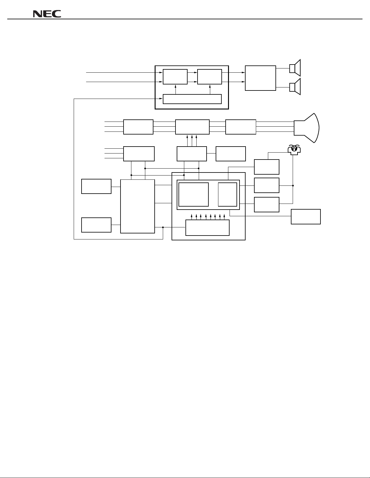
SYSTEM BLOCK DIAGRAM
TV
••••
µµµµ
PC1857A
PD17052
µ
µ
PD17053
PC2800A
µ
Tuner PIF & SIF
DTS interface
µ
PC1854
(US-MTS)
Tuning
microcontroller
Remote control
reception amplifier
PIN photo diode
MTS
decoder
Color, intensity, and
deflecting signal
processor
PC1857A
µ
L
Surround
R
I2C bus interface
Volume
Balance
Tone
RGB
output
Vertical
output
Horizontal
output
Power
amplifier
µ
PC1316C
CRT
Speaker
L
R
Remark
DTS: Digital Tuning System
MTS: Multichannel Television Sound
2
Page 3
• PC monitor
Sound input
L
R
Signal input
R
G
B
RGB
input
processor
PC18757A
µ
Surround
2
C bus interface
I
Video
amplifier
Volume
Balance
Tone
RGB
drive
Power
amplifier
PC1316C
µ
µµµµ
PC1857A
Speaker
L
R
CRT
V.sync
H.sync
C.sync
Panel
switch
EEPROM
TM
Sync. signal
separator
HD VD
Microcontroller
µ
PD78014Y
Control
H-F/V
OSD
Sync. signal
processor
D/A converter
µ
PC6221
µ
PC1885
µ
PC1883
PLL
Gometry
compensation
Deflection
compensation drive
Vertical
drive
Horizontal
drive
Yoke
High-voltage
unit
3
Page 4
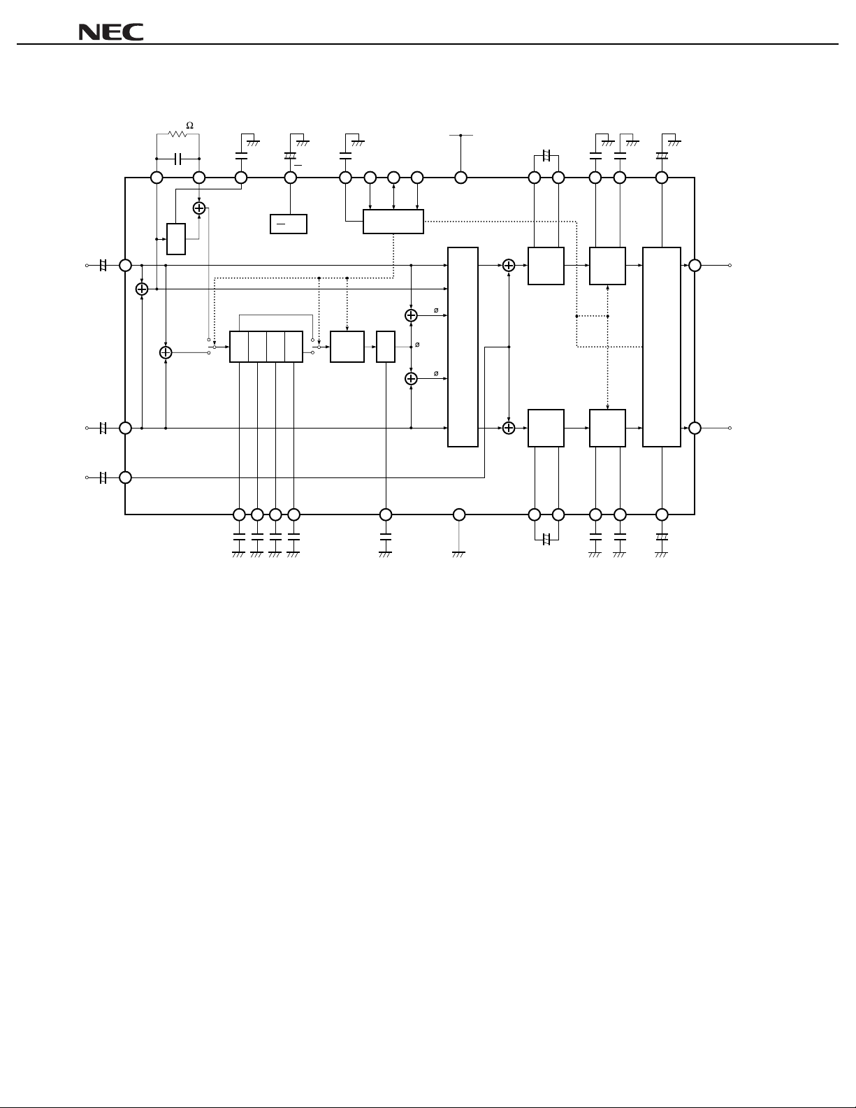
BLOCK DIAGRAM
820 k
µµ
0.082
MFO
29 30 28 24 23 22 21 20 15 19 18 10
F
680 pF
MFI LF1
+
µµµµ
PC1857A
22
F
1
+
V
CC
DGND
2
ADS SDA SCL
12 V
VCC
2.2+F
µ
OFL1 OFL2
µ
0.047 F
LBC LTC VOL-C
3300 pF
9 17
3.3 F
µ
Lin
+
26
+
µ
2.2 F
+
Rin
+
27
2.2 F
µ
MIX
+
25
µ
2.2 F
-
LPF
-
+
FC1 FC2 FC3 FC4 OFR1 OFR2
µ
0.1 F 0.022 1000 pFF 0.047 3300 pFF 3.3 F
1
V
2
Phase shifter
0.0222200 pF F
CC
Effect
control
µ
µ
I2C bus
interface
L
L + R
+
L +
+
LPFPS1PS2 PS3 PS4
-
+
65432 81211
LF2 AGND RBC RTC BAL-C
Output
select
R
-
R
1
Offset
+
absorption
+
+
+
Offset
absorption
+
2.2 F
µ
Tone
control
Volume,
balance
control/
mute
Tone
control
7 16
+
µ
µ
Lout
14
Rout
13
4
Page 5
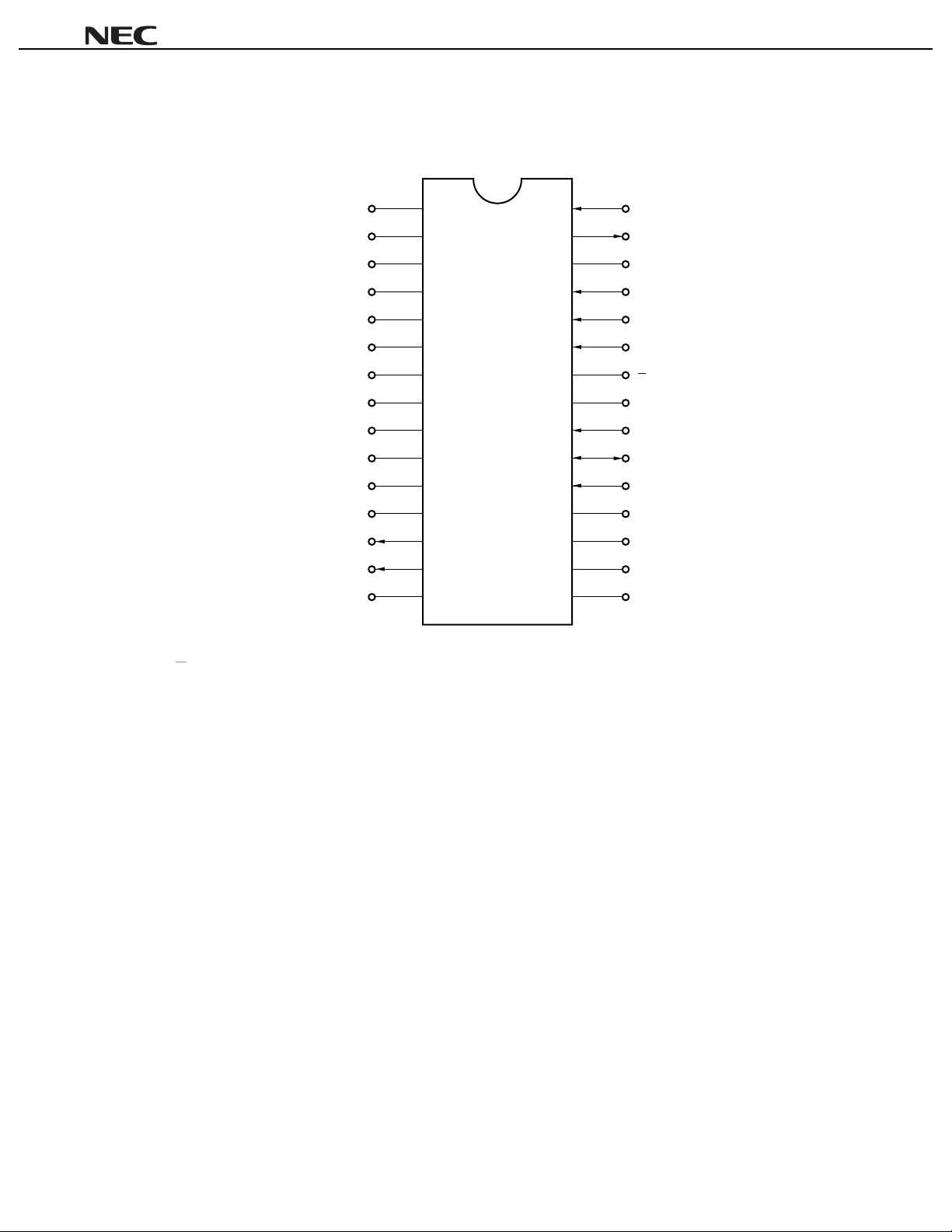
PIN CONFIGURATION (Top View)
30-pin plastic shrink DIP (400 mil)
µµµµ
PC1857A
30
29
28
27
26
25
24
23
22
21
20
19
18
17
16
MFI
MFO
LF1
Rin
Lin
MIX
1
CC
V
2
DGND
ADS
SDA
SCL
OFL1
OFL2
VOL-C
BAL-C
1
V
2
CC
AGND
FC1
FC2
FC3
FC4
LF2
RTC
RBC
LTC
LBC
OFR1
OFR2
Rout
Lout
V
CC
1
2
3
4
5
6
7
8
9
10
11
12
13
14
15
: Reference Voltage Filter MFO : Monaural Filter Output
ADS : Slave Address Select MIX : Mixer Input
AGND : Analog Ground OFL1, OFL2 : L-channel Offset Absorption
BAL-C : Balance Control Offset Absorption OFR1, OFR2 : R-channel Offset Absorption
DGND : Ground for I2C Bus RBC : R-channel Bass Capacitor
FC1-FC4 : Phase Shift Filter Rin : R-channel Signal Input
LBC : L-channel Bass Capacitor Rout : R-channel Signal Output
LF1, LF2 : Low-pass Filter RTC : R-channel Treble Capacitor
Lin : L-channel Signal Input SCL : Serial Clock for I2C Bus
Lout : L-channel Signal Output SDA : Serial Data for I2C Bus
LTC : L-channel Treble Capacitor V
CC
: Power Supply
MFI : Monaural Filter Input VOL-C : Volume Control Offset Absorption
5
Page 6

µµµµ
PC1857A
CONTENTS
1. PIN FUNCTIONS.............................................................................................................................. 7
2. ATTENTIONS.................................................................................................................................... 14
2
3. I
C BUS INTERFACE...................................................................................................................... 15
3.1 Data Transfer.......................................................................................................................................... 15
3.1.1 Start condition............................................................................................................................ 15
3.1.2 Stop condition............................................................................................................................ 16
3.1.3 Data transfer.............................................................................................................................. 16
3.2 Data Transfer Format............................................................................................................................. 17
3.2.1 1-byte data transfer.................................................................................................................... 18
3.2.2 Successive data transfer............................................................................................................ 18
3.2.3 Acknowledge.............................................................................................................................. 18
4. EXPLANATION OF EACH COMMAND ........................................................................................ 19
4.1 Subaddress List..................................................................................................................................... 19
4.2 Initialization............................................................................................................................................ 20
4.3 Surround Function................................................................................................................................. 20
4.4 Explanation of Each Command............................................................................................................ 21
4.4.1 Mute........................................................................................................................................... 21
4.4.2 Output selection......................................................................................................................... 21
4.4.3 Surround mode .......................................................................................................................... 22
4.4.4 Surround effect .......................................................................................................................... 23
4.4.5 Mix ............................................................................................................................................. 23
4.4.6 Automatic increment.................................................................................................................. 24
4.4.7 Volume level .............................................................................................................................. 25
4.4.8 Balance...................................................................................................................................... 25
4.4.9 Bass level................................................................................................................................... 26
4.4.10 Treble level ................................................................................................................................ 26
5. ELECTRICAL CHARACTERISTICS ............................................................................................... 27
6. CHARACTERISTIC CURVES.......................................................................................................... 33
6.1 Frequency Characteristic in Each Mode.............................................................................................. 33
6.2 Control Characteristic........................................................................................................................... 36
6.3 I/O Characteristic................................................................................................................................... 38
7. PACKAGE DRAWING..................................................................................................................... 39
8. RECOMMENDED SOLDERING CONDITIONS ............................................................................. 40
6
Page 7
µµµµ
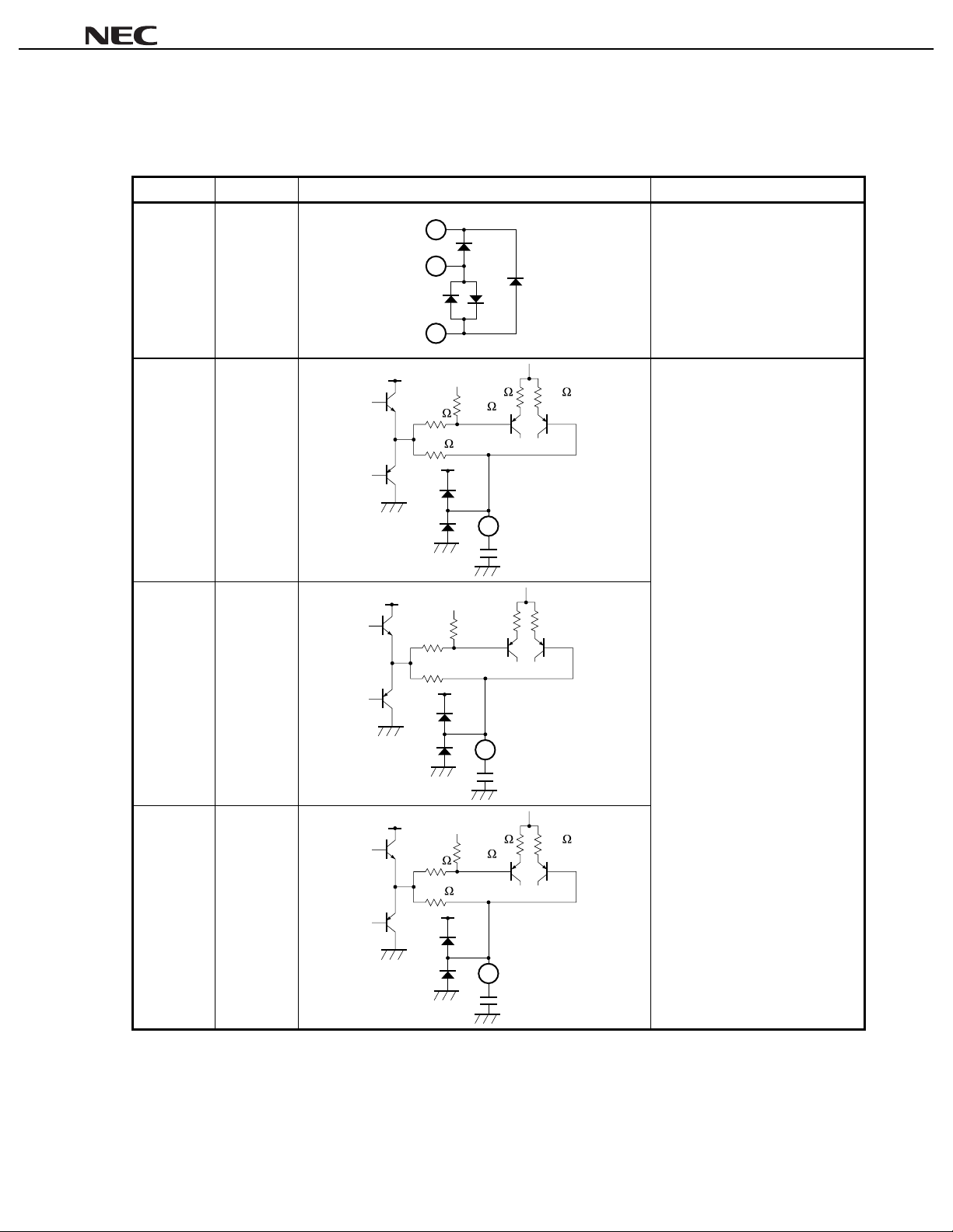
1. PIN FUNCTIONS
Table 1-1. Pin Function List (1/7)
Pin Number Pin Name Equiv al ent Circuit Description
1AGND
2FC1
15
1
23
V
CC
36 k
18 k
3 k 3 k
36 k
V
CC
Ground for analog signal.
Pin voltage: approx. 0. 0 V
Connection pin for capacitor whi ch
determines time constant of phase
shifter.
Pin voltage: approx. 6. 0 V
PC1857A
3FC2
4FC3
V
CC
36 kΩ
18 kΩ
V
CC
36 k
18 k
2
3 kΩ 3 kΩ
36 kΩ
V
CC
3
3 k 3 k
36 k
V
CC
4
0.1 F
µ
2200 pF
Remark
Pin voltage is the reference value when V
CC
= 12 V.
0.022 F
µ
7
Page 8
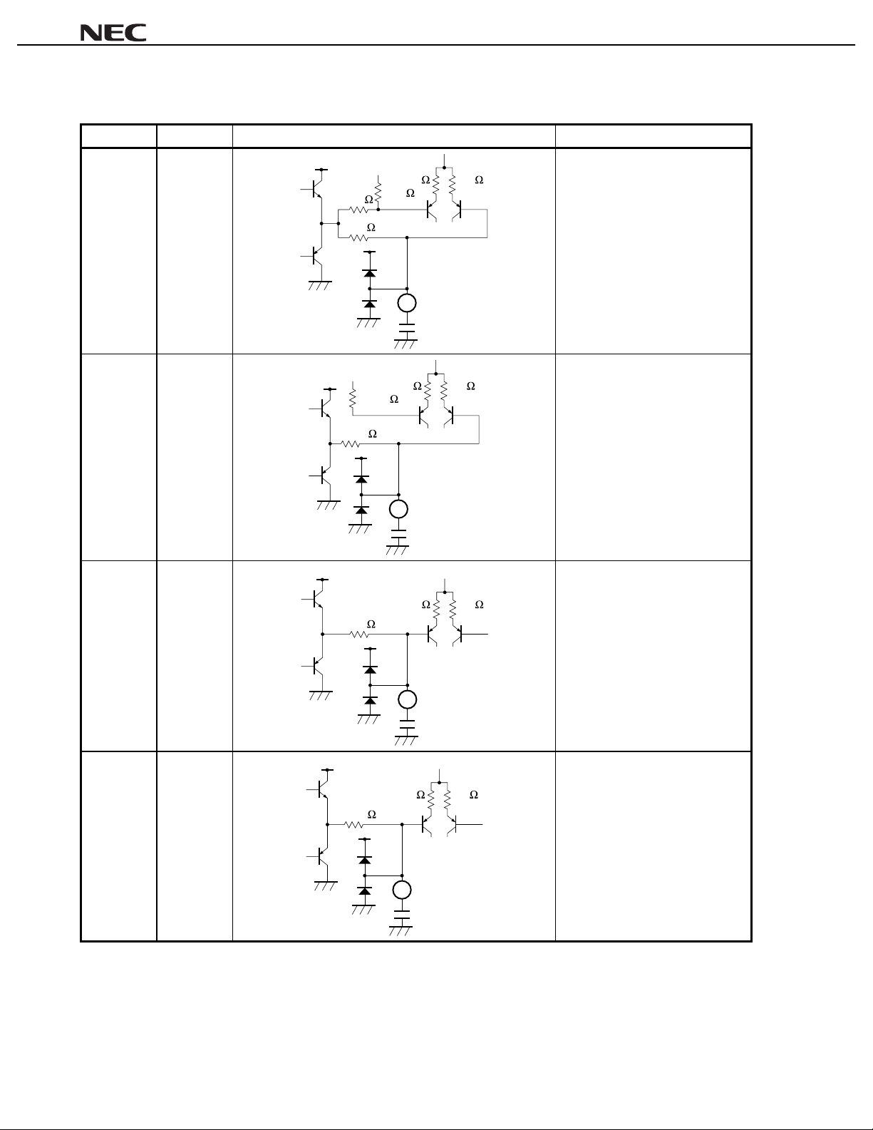
Table 1-1. Pin Function List (2/7)
Pin Number Pin Name Equiv al ent Circuit Description
V
5FC4
CC
3 k 3 k
36 k
36 k
18 k
V
CC
5
µ
0.022 F
Connection pin for capacitor whi ch
determines time constant of phase
shifter.
Pin voltage: approx. 6. 0 V
µµµµ
PC1857A
6LF2
7RTC
8RBC
V
CC
17.7 k
17.7 k
VCC
12 k
V
CC
13.8 k
5 k 5 k
V
CC
6
VCC
3 k 3 k
V
CC
1000 pF
3 k 3 k
7
3300 pF
Low-pass filter.
Pin voltage: approx. 6. 0 V
Connection pin for capacitor for
treble boost/cut frequenc y
characteristic of R-channel signal.
Pin voltage: approx. 6. 0 V
Connection pin for capacitor for
bass boost/cut f requenc y
characteristic of R-channel signal.
Pin voltage: approx. 6. 0 V
Remark
8
Pin voltage is the reference value when V
8
0.047 F
CC
= 12 V.
µ
Page 9
µµµµ
PC1857A
Table 1-1. Pin Function List (3/7)
Pin Number Pin Name Equiv al ent Circuit Description
V
9LTC
CC
Connection pin for capacitor for
treble boost/cut frequenc y
12 k
3 k 3 k
V
CC
9
3300 pF
characteristic of L-channel signal.
Pin voltage: approx. 6. 0 V
10 LBC
VCC
Connection pin for capacitor for
bass boost/cut f requenc y
13.8 k
3 k 3 k
VCC
10
0.047 F
µ
characteristic of L-channel signal.
Pin voltage: approx. 6. 0 V
11 OFR1 Pin that absorbs offset voltage of R
channel.
V
12 OFR2
+
11
µ
2.2 F
12
CC
V
V
5 k
CC
CC
5 k
6 k
1/2V
CC
60 k
5 k
6 k
3 k
3 k
Pin voltage: approx. 6. 0 V
Remark
Pin voltage is the reference value when V
CC
= 12 V.
9
Page 10
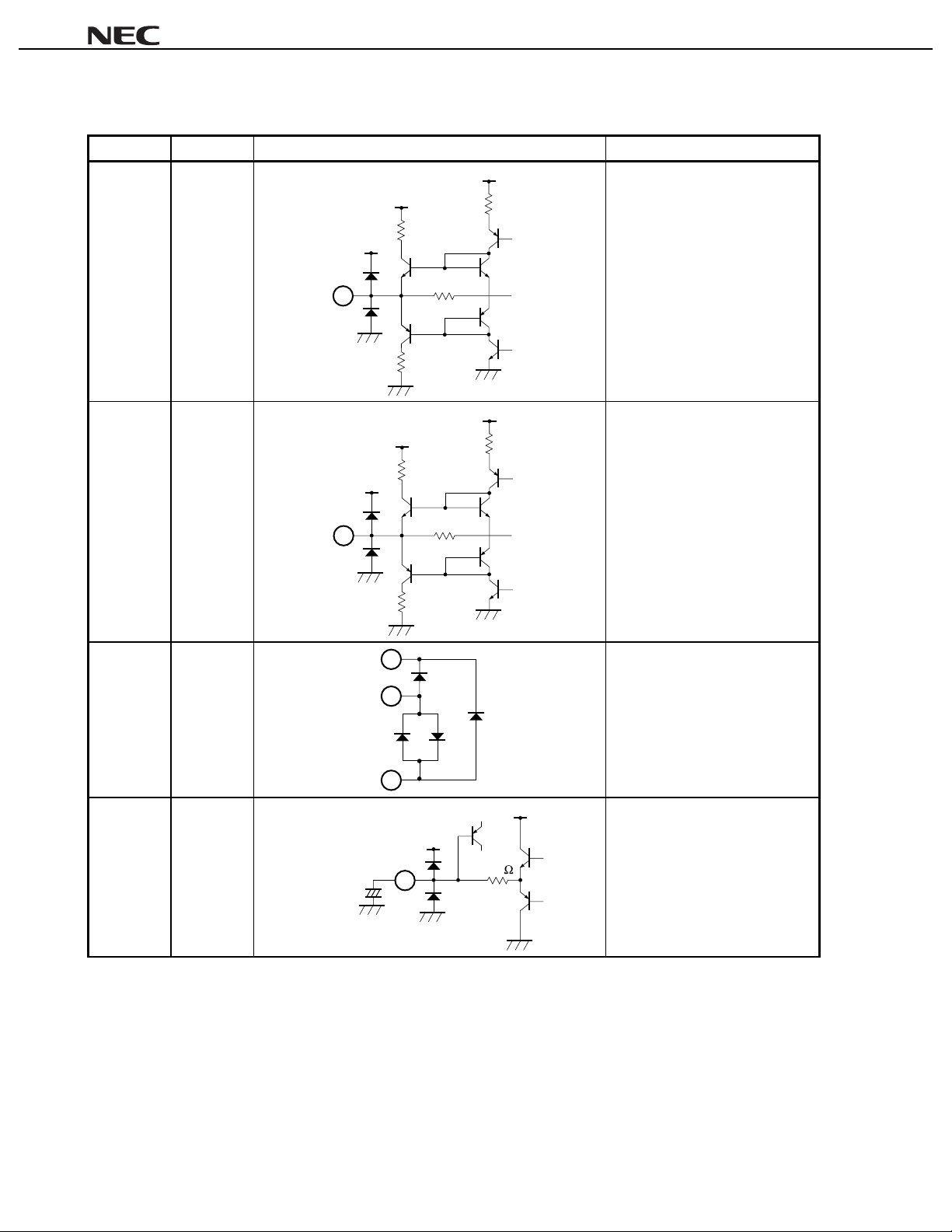
Table 1-1. Pin Function List (4/7)
Pin Number Pin Name Equiv al ent Circuit Description
V
13 Rout
V
CC
2 kΩ
V
CC
CC
3 kΩ
R-channel signal output pin.
Pin voltage: approx. 6. 0 V
µµµµ
PC1857A
14 Lout
15 V
CC
13
14
10 kΩ
2 kΩ
V
CC
V
CC
3 kΩ
L-channel signal output pin.
Pin voltage: approx. 6. 0 V
2 kΩ
V
CC
10 kΩ
2 kΩ
15
Supply voltage.
Pin voltage: approx. 12. 0 V
1
16 BAL-C
Remark
10
23
16
3.3 F
+
µ
Pin voltage is the reference value when V
V
CC
CC
= 12 V.
50 k
V
CC
Pin for D/A convert er capacitor for
balance control.
Pin voltage: approx. 4. 8 V
Page 11
µµµµ
PC1857A
Table 1-1. Pin Function List (5/7)
Pin Number Pin Name Equiv al ent Circuit Description
V
50 k
3 k
6 k
CC
Pin for D/A convert er capacitor for
volume control.
Pin voltage: approx. 6. 0 V
3 k
channel.
Pin voltage: approx. 6. 0 V
17 VOL-C
V
CC
17
+
µ
3.3 F
18 OFL2 Pin that absorbs offset voltage of L
1/2V
CC
60 k
6 k
19 OFL1
+
2.2 F
18
µ
V
CC
V
CC
V
5 k
CC
20 SCL
21 SDA
22 ADS
19
20
22
21
5 k
5 kΩ
5 kΩ
5 k
Serial clock line (I2C bus clock Input)
pin.
Pin voltage: approx. 0. 0 V
Serial data line (I2C bus data I/O)
pin
Pin voltage: approx. 0. 2 V
5 kΩ
Slave address select pi n.
Pin voltage: approx. 0. 0 V
23 DGND
Remark
Pin voltage is the reference value when V
15
23
GND for I2C bus signal.
Pin voltage: approx. 0. 0 V
1
CC
= 12 V.
11
Page 12
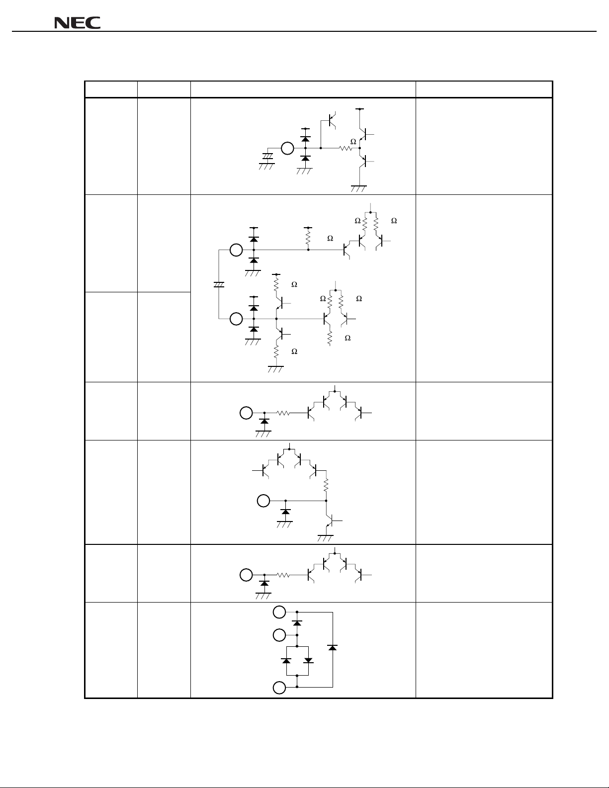
Table 1-1. Pin Function List (6/7)
Pin Number Pin Name Equiv al ent Circuit Description
24 V
1
2
CC
22+F
µ
24
V
CC
5 k
V
CC
Filter pin for middle point of s uppl y
voltage.
Pin voltage: approx. 6. 0 V
V
CC
20 k
90 k
20 k
µµµµ
PC1857A
25 MIX
26 Lin
27 Rin
2.2 F
µ
µ
2.2 F
25
MIX
26
Lin
1/2V
CC
V
CC
3 k 3 k
60 k
Mixing signal input pin.
Input impedance: 60 kΩ
Pin voltage: approx. 6. 0 V
5 k
+
1/2V
CC
V
CC
3 k 3 k
60 k
L-channel signal input pin.
Input impedance: 60 kΩ
Pin voltage: approx. 6. 0 V
5 k
+
1/2V
CC
V
CC
3 k 3 k
60 k
R-channel signal input pin.
Input impedance: 60 kΩ
Pin voltage: approx. 6. 0 V
Remark
12
27
2.2 F
+
µ
Rin
Pin voltage is the reference value when V
CC
= 12 V.
5 k
Page 13
µµµµ
PC1857A
Table 1-1. Pin Function List (7/7)
Pin Number Pin Name Equiv al ent Circuit Description
28
18 kΩ
V
29
CC
V
CC
5 kΩ 5 kΩ
1 k
18 k
Low-pass filter.
Pin voltage: approx. 6. 0 V
function (simulated m ode) (see 4.3
Surround Function).
Pin voltage: approx. 6. 0 V
28 LF1
680 pF
29 MFO Filter output pin for surround
30
µ
V
CC
CC
= 12 V.
15 k
47 k
(simulated mode) (see 4.3
Surround Function).
Pin voltage: approx. 6. 0 V
30 MFI Filter input pin for surround function
Remark
Pin voltage is the reference value when V
820 k 0.082 F
13
Page 14

2. ATTENTIONS
(1) Attention on Pop Noise Reduction
When changing the surround mode, use the mute function (approx. 200 ms) for pop noise reduction (see
).
Mute
When turning ON/OFF power to the
(2) Attention on Supply Voltage
Drive data on the I2C bus after supply voltage of total application system becomes stable.
PC1857A, use the external mute function for pop noise reduction.
µ
µµµµ
PC1857A
4.4.1
14
Page 15

µµµµ
PC1857A
3. I2C BUS INTERFACE
The µPC1857A has serial bus function.
This serial bus (I2C bus) is a double-wired bus developed by Philips. It is composed of 2 wires: serial clock line
(SCL) and serial data line (SDA).
The µPC1857A has built-in I2C bus interface circuit, and five rewritable registers (8 bits).
SCL (Serial Clock Line)
The host CPU outputs a serial clock to synchronize with the data. The µPC1857A takes in the serial data based
on this clock.
Input level is compatible with CMOS.
Clock frequency is 0 to 100 kHz.
SDA (Serial Data Line)
The host CPU outputs the data which is synchronized with the serial clock. The µPC1857A takes in this data
based on the clock.
Input level is compatible with CMOS.
Figure 3-1. Internal Equivalent Circuit of Interface Pin
R
SCL
SDA
PC1857A
µ
p
R
p
3.1 Data Transfer
3.1.1 Start condition
Start condition is made by SDA falling from “High” to “Low” while SCL is “High” as shown in Figure 3-2.
When this start condition is received, the
PC1857A takes in the data synchronized with the serial clock after that.
µ
15
Page 16

3.1.2 Stop condition
Stop condition is made by SDA rising from “Low” to “High” while SCL is “High” as shown in Figure 3-2.
When this stop condition is received, the
PC1857A stops taking in or outputting data.
µ
Figure 3-2. Start/Stop Condition of Data Transfer
3.5 V
SDA
1.5 V
µµµµ
PC1857A
4.7 s
µ
MIN.
Stop
SCL
Start
4.0 s
µ
MIN.
3.5 V
1.5 V
3.1.3 Data transfer
When transferring data, the data must be changed while SCL is “Low” as shown in Figure 3-3. Never change the
data while SCL is “High”.
Figure 3-3. Data Transfer
SDA
Note 1
Note 2
Notes 1.
Remark
16
SCL
Data hold time for I
Data setup time: 250 ns MIN.
2.
Clock frequency: 0 to 100 kHz
2
C device: 300 ns MIN., Data hold time for CPU: 5 µs MIN.
Page 17

3.2 Data Transfer Format
Figure 3-4 shows an example of data transfer in write mode.
Figure 3-4. Example of Data Transfer in Write Mode
SDA
SCL
Slave address
D6
D5 D4 D3 D2D1 D0
W
ACK ACK
Subaddress
D7 D6 D5D4 D3 D2 D1 D0
SA
µµµµ
PC1857A
0
D7 D6 D5D4 D3 D2 D1 D0
Data
ACK
Remark
W: Write mode, ACK: Acknowledge bit
Data is composed of 8 bits. One acknowledge bit always follows these 8 bits of data. Data must be transferred
starting from the MSB.
The 1 byte immediately following the start condition specifies a slave address (chip address). This slave address
is composed of 7 bits.
Table 3-1 shows the slave address of the
Table 3-1. Slave Address of
Bias Voltage of ADS (P i n 22)
5 V 10001 1 0
GND 10001 0 0
The user can set bit D1 freely.
Note
PC1857A. This slave address is registered by Philips.
µ
PC1857A
µ
Slave Address
Note
D6 D5 D4 D3 D2
D1
D0
0: Bias voltage of ADS (pin 22) is 0 V.
1: Bias voltage of ADS (pin 22) is 5 V.
The 1 bit following the slave address is a read/write bit which specifies the direction of the data to be subsequently
transferred. Write “0” to this read/write bit because the
PC1857A is write mode only.
µ
The byte following the slave address is the subaddress byte of the µPC1857A.
The µPC1857A has five subaddresses, from SA0 to SA4, and each of these addresses is composed of 8 bits. The
data to be set to a subaddress follows this subaddress byte.
17
Page 18

3.2.1 1-byte data transfer
The format in which 1-byte data is to be transferred is as follows:
µµµµ
PC1857A
Start Slave address Subaddress Data Stop
3.2.2 Successive data transfer
The
PC1857A has an automatic increment function which can be used to transfer successive data (refer to
µ
Automatic increment
By using this function, the internal subaddress is automatically incremented if a slave address and a subaddress
have been set, so that the data from subsequent subaddresses can be transferred in succession.
Incrementing the subaddress of the µPC1857A is stopped when the subaddress reaches “04H”.
The format in which 5 bytes of data are to be transferred in succession by using the automatic increment function
is as follows:
Start Slave address Subaddress Data 1
The host CPU transfers “00H” as subaddress SA0 after start and slave addresses, as shown above. Data SA0 is
transferred after this subaddress SA0, and without transferring the stop condition the data SA1, SA2, SA3, and SA4 are
transferred successively, and then the stop condition is transferred.
To successively change data at a fixed subaddress, for example to turn up/down the volume, turn off the
automatic increment function.
).
Write
mode
Write
ACK ACK ACK
mode
Data 2 Data 5 StopACK ACK ACK ACK ACK
4.4.6
3.2.3 Acknowledge
On the I2C bus, an acknowledge bit is appended to the 9th bit following the data. This acknowledge bit is used to
judge whether data transfer has been successful. The host CPU judges whether data transfer has been successful
or not, depending on whether the status of the acknowledge bit is “H” or “L”.
When the acknowledge bit is “L”, it indicates success. When the acknowledge bit is “H”, it indicates failure of
transfer or forced release of bus (NAK status). The NAK status occurs when a wrong slave address is transferred to
a slave IC or data transfer from slave side is finished in the read status.
18
Page 19

4. EXPLANATION OF EACH COMMAND
4.1 Subaddress List
µµµµ
PC1857A
Bit
Subaddress
00H Output mute
01H Mix
02H 0 Automatic
03H 0 Automatic
04H 0 Automatic
MSB
D7
0: OFF
1: ON
0: OFF
1: ON
D6 D5 D4 D3 D2 D1
0 Output select
D5 D4 Lout Rout
00 L R
01 L L
10 R R
1 1 L + R L + R
Automatic
increment
0: OFF
1: ON
increment
0: OFF
1: ON
0 Bass level
increment
0: OFF
1: ON
0 Treble level
increment
0: OFF
1: ON
Volume level
Volume : MAX to MIN
Data : 111111 to 000000
Balance
L volume : MIN to MAX to MAX
R volume: MAX to MAX to MIN
Data : 111111 to 100000 to 000000
Gain : Boost to 0 to Cut
Data : 11111 to 10000 to 00000
Gain : Boost to 0 to Cut
Data : 11111 to 10000 to 00000
Surround mode
D3 D2 Mode
00 Simulated
01 Music
10 Movie
11OFF
LSB
D0
Surround effect
D1 D0 Gain
0 0 0 dB
01
10
11
3 dB
−
6 dB
−
12 dB
−
Cautions 1. Be sure to write “0” to bit D7 of subaddresses 02H through 04H, bit D6 of subaddress 00H,
and bit D5 of subaddresses 03H and 04H.
2. The surround mode is OFF: 00H (D3, D2 = 11) in any mode other than stereo mode is
selected for output: 00H (D5, D4 = 00).
19
Page 20

4.2 Initialization
After power application, be sure to initialize the subaddresses as shown below.
µµµµ
PC1857A
Table 4-1. Initialization of
Bit
Subaddress
00H 00001100
01H 0
02H 0
03H 0
04H 0
MSB
D7
D6 D5 D4 D3 D2 D1
−−−−−−−
−
−
−
PC1857A (recommendation value)
µµµµ
100000
010000
010000
Caution Until initialization is completed, mute using an external unit.
Remark
: Don’t care.
−
4.3 Surround Function
For how to set the surround mode, refer to the table below.
Table 4-2. Setting Surround Mode
LSB
D0
Setting Subaddress: 00H Description
Surround Mode D3 D2 Units of P hase Shifter Effect
Simulated 0 0 4 units Monaural to pseudo-stereo
Music 0 1 1 unit Stereo sound to surround
Movie 1 0 4 units
OFF 1 1
−
Through
Caution When changing the surround mode, use the mute function (approx. 200 ms) for pop noise
reduction.
20
Page 21

µµµµ
PC1857A
4.4 Explanation of Each Command
4.4.1 Mute
The mute function can be turned ON/OFF by using data of bit D7 of subaddress 00H.
Figure 4-1. Mute
D7 D6 D5 D4 D3 D2 D1 D0
Subaddress
Caution When changing the surround mode, and when turning ON/OFF power, use the mute function
00H Mute Output selection0
Output mute
01Mute: OFF
Mute: ON
(approx. 200 ms) for pop noise reduction.
Surround mode Surround effect
4.4.2 Output selection
Output can be selected by using data of bits D5 and D4 of subaddress 00H.
Figure 4-2. Output Selection
D7 D6 D5 D4 D3 D2 D1 D0
Subaddress
00H Mute Output selection0
Surround mode Surround effect
Output selection
D5
D4
Lout
0
0
L
0
1
L
1
0
R
1
1
L + R
OutputData
Rout
R
L
R
L + R
Caution The surround mode is OFF (D3, D2 = 11) in modes other than the stereo mode (D5, D4 = 00).
21
Page 22

µµµµ
PC1857A
4.4.3 Surround mode
The following surround modes can be selected by using data of bits D3 and D2 of subaddress 00H.
Simulated : Simulated stereo sound for monaural source. The difference between the signal that has gone
through HPF and the signal that has gone through LPF is calculated, and the phase of the
difference is shifted and added to the original signal. The simulated stereo effect is created if the
output frequency characteristics of the L-channel and R-channel signals is comb-shaped.
Music : Surround sound for stereo source. The phase of the differential signal between L and R channels
(L-R signal) is rotated by a phase shifter (1-unit), and is added to the original signal.
Movie : Surround sound for stereo source. The phase of the differential signal between L and R channels
(L-R signal) is rotated by a phase shifter (4-unit), and is added to the original signal.
OFF : Original signal as is.
Figure 4-3. Surround Mode
D7 D6 D5 D4 D3 D2 D1 D0
Subaddress
00H Mute Output selection0
Surround mode Surround effect
Surround mode
Data
D3
0
0
1
1
D2
0
1
0
1
Mode
Simulated
Music
Movie
OFF
Caution The surround mode is OFF (D3, D2 = 11) if the stereo mode is not selected by the output
selection bits (D5, D4 = 00).
22
Page 23

µµµµ
PC1857A
4.4.4 Surround effect
The surround effect can be changed in four steps by using the data of bits D1 and D0 of subaddress 00H.
Figure 4-4. Surround Effect
D7 D6 D5 D4 D3 D2 D1 D0
Subaddress
00H Mute Output selection0
Surround mode Surround effect
Surround effect
Data
D1
0
0
1
1
D0
Gain
0
0 dB
-
3 dB
1
-
6 dB
0
-
12 dB
1
4.4.5 Mix
Mixing of the signal input to the MIX pin can be turned ON/OFF by using the data of bit D7 of subaddress 01H.
Subaddress
01H Mix
Figure 4-5. Mix
D7 D6 D5 D4 D3 D2 D1 D0
Automatic
increment
Mix
01Mix: OFF
Mix: ON
Volume level
23
Page 24

µµµµ
PC1857A
4.4.6 Automatic increment
The automatic increment function can be turned ON/OFF by using the data of bit D6 of subaddresses 01H through
04H.
This is effective when transmitting data successively (refer to
Figure 4-6. Automatic Increment
D7 D6 D5 D4 D3 D2 D1 D0
Subaddress
01H-04H Don't care
Caution Subaddress 00H does not have an automatic increment function. It is always set to ON.
The automatic increment function automatically increments the subaddress when data is transferred successively.
Automatic increment ON : The subaddress is automatically incremented immediately after byte data with D6 = 1
Automatic increment OFF : The subaddress is fixed immediately after byte data with D6 = 0 has been
Automatic
increment
Automatic increment
01Automatic increment: OFF
Automatic increment: ON
has been transferred.
This setting is useful if the data at every subaddress is to be set at once for
initialization. The subaddress is always incremented immediately after the data of
subaddress: 00H has been transferred.
transferred. This setting is useful when the data at the same subaddress is to be
successively changed, for example to turn up/down the volume.
3.2.2 Successive data transfer
Don't care
).
There is an automatic increment function ON/OFF bit in subaddresses 01H through 04H. Incrementing
subaddresses is individually controlled by the automatic increment function ON/OFF bit of each subaddress.
For example, if the automatic increment function of subaddress 01H is turned ON, and that of subaddress 02H is
turned OFF, the subaddress is automatically incremented from 01H to 02H, and is fixed to 02H.
Even if the automatic increment function ON/OFF bit of subaddress 04H is set to ON, the subaddress is not
incremented. If the next data is transferred after the data of 04H has been set (acknowledge bit: L), acknowledge
enters the NAK status (acknowledge bit: H), and data transfer from the host CPU is stopped.
24
Page 25

µµµµ
PC1857A
4.4.7 Volume level
The volume of output can be controlled in 64 steps by using the data of bits D5 through D0 of subaddress 01H.
Figure 4-7. Volume Level
D7 D6 D5 D4 D3 D2 D1 D0
Subaddress
01H Mix
Automatic
increment
Volume level
Volume level
Data
D5-D0
000000
to
111111
Volume
MIN.
to
MAX.
4.4.8 Balance
The balance of output of the Lout and Rout pins can be controlled in 64 steps by using the data of bits D5 through
D0 of subaddress 02H.
Subaddress
02H 0
Figure 4-8. Balance
D7 D6 D5 D4 D3 D2 D1 D0
Automatic
increment
Balance
Balance
Data Volume
D5-D0
000000
to
100000
to
111111
Lout
MAX.
to
MAX.
to
MIN.
Rout
MIN.
to
MAX.
to
MAX.
25
Page 26

µµµµ
4.4.9 Bass level
The bass level of output can be controlled in 32 steps by using the data of bits D4 through D0 of subaddress 03H.
Figure 4-9. Bass Level
D7 D6 D5 D4 D3 D2 D1 D0
Subaddress
03H 0 0
Automatic
increment
Bass level
Bass level
Data
D4-D0
00000
to
10000
to
11111
Gain
Cut
to
0
to
Boost
PC1857A
4.4.10 Treble level
The treble level of output can be controlled in 32 steps by using the data of bits D4 through D0 of subaddress
04H.
Figure 4-10. Treble Level
D7 D6 D5 D4 D3 D2 D1 D0
Subaddress
04H 0 0
Automatic
increment
Treble level
Treble level
Data
D4-D0
00000
to
10000
to
11111
Gain
Cut
to
0
to
Boost
26
Page 27

5. ELECTRICAL CHARACTERISTICS
µµµµ
PC1857A
Absolute Maximum Ratings (Unless otherwise specified, TA = 25
C)
°°°°
Parameter Symbol Condition Rating Unit
Supply voltage V
Input signal voltage V
I2C bus input signal voltage V
Permissible package di ssipation P
Operating temperature T
Storage temperature T
CC
CNT
stg
Without signal 14.0 V
IN
Pins Lin, Rin, MIX V
CC
Pins SDA, SCL VCC + 0.2 V
D
TA = 75 °C 500 mW
A
VCC = 12 V
20 to +75
−
40 to +125
−
V
C
°
C
°
Caution If any of the parameters exceeds the absolute maximum ratings, even momentarily, the quality of
the product may be impaired. The absolute maximum ratings are values that may physically
damage the product(s). Be sure to use the product(s) within the ratings.
Recommended Operating Conditions (Unless otherwise specified, TA = 25
Parameter Symbol Condition
Supply voltage V
Input signal voltage V
I2C bus input voltage (H) V
I2C bus input voltage (L) V
CC
cntH
cntL
Gain between input and output: 0 dB 8.1 12.0 13.2 V
IN
VCC = 12 V, gain between input and output: 0 dB 0.0 1.4 7.9 V
Pins SDA, SCL 3.5 5.0 6.0 V
C)
°°°°
Rating
MIN. TYP. MAX.
0.1 0 +1.5 V
−
Unit
p-p
27
Page 28

Electrical Characteristics (1/5)
(Unless otherwise specified, V
CC
= 12 V, TA = 25 °C, RH ≤ 70%, f = 1 kHz, VIN = 0.5 V
r.m.s.
, no load)
µµµµ
PC1857A
Parameter Sym bol Test Condition
Circuit current I
Maximum input voltage
Lin → Lout
Maximum input voltage
Rin → Rout
Distortion rate
Lin → Lout
Distortion rate
Rin → Rout
Voltage gain
Lin → Lout
Voltage gain
Rin → Rout
Voltage gain
MIX → Lout
Voltage gain
CC
No signal 0D 3F 20 10 10 12 18 25 mA
VOM-L Lin = variable (t ested)
Lout = THD 1%
VOM-R Rin = variable (tested)
Rout = THD 1%
THDL Lin = 2.0 V
Rin = GND
THDR Lin = GND
Rin = 2.0 V
GV-LL Lin = 0.5 V
Rin = GND
GV-RR Lin = GND
Rin = 0.5 V
GV-ML MIX = 0.5 V
Lin, Rin = GND
GV-MR 5.0 6.0 7.0 dB
MIX → Rout
Ripple rejection ratio
CC
→ Lout
V
Ripple rejection ratio
CC
→ Rout
V
Output noise voltage
(surround OFF)
SVRR-L 0D14201010
SVRR-R
Vn-L
(OFF)
VCC = 100 mV
f = 100 Hz
Lin, Rin = GND
Rg = 0 Ω, JIS-A 0D3F201010
Lout
Output noise voltage
(surround OFF)
Vn-R
(OFF)
Rout
Cross talk
Lin → Rout
Cross talk
Rin → Lout
CT-L Lin = 0.5 V
Rin = GND
CT-R Lin = GND
Rin = 0.5 V
r.m.s.
r.m.s.
r.m.s.
r.m.s.
r.m.s.
r.m.s.
r.m.s.
r.m.s.
Subaddress Data Rating
Unit
00 01 02 03 04 MIN. TY P. MAX.
0D 3F 20 10 10 2.8 3.1
2.8 3.1
0D 2B 20 10 10
0.1 0.5 %
−
0.1 0.5 %
−
r.m.s.
V
−
r.m.s.
V
−
0D 3F 20 10 10−1.0 0 +1.0 dB
1.0 0 +1.0 dB
−
0D BF 20 10 10 5.0 6.0 7.0 dB
50 dB
50 dB
V
50
µ
V
50
µ
70 dB
70 dB
0D 3F 20 10 10
−−−
−−−
−−
−−
−−80−
−−80−
r.m.s.
r.m.s.
28
Page 29

Electrical Characteristics (2/5)
(Unless otherwise specified, V
CC
= 12 V, TA = 25 °C, RH ≤ 70%, f = 1 kHz, VIN = 0.5 V
r.m.s.
µµµµ
, no load)
PC1857A
Parameter Sym bol Test Condition
Volume attenuation 1
Lin → Lout1
Volume attenuation 2
VOL-L1 Lin = 0.5 V
Rin = GND
VOL-L2 20
Lin → Lout2
Volume attenuation 3
VOL-L3 00
Lin → Lout3
Volume attenuation
deviation
Rin → R/Lout1
Volume attenuation
deviation
Rin → R/ Lout2
Volume attenuation
deviation
Rin → R/ Lout3
Mute attenuation
Lin → Lout
Mute attenuation
Rin → Rout
Balance attenuation L1
Lin → Lout1
Balance attenuation L2
VOL-RL1 Lin = GND
Rin = 0.5 V
Difference from VOL-L1
VOL-RL2 Lin = GND
Rin = 0.5 V
Difference from VOL-L2
VOL-RL3 Lin = GND
Rin = 0.5 V
Difference from VOL-L3
MUTE-L Lin = 2.0 V
Rin = GND
MUTE-R Lin = GND
Rin = 2.0 V
BAL-L1 Lin = 0.5 V
Rin = GND
BAL-L2 28
Lin → Lout2
Balance attenuation L3
BAL-L3 30
Lin → Lout3
Balance attenuation L4
BAL-L4 3F
Lin → Lout4
Balance attenuation R1
Rin → Rout1
Balance attenuation R2
BAL-R1 Lin = GND
Rin = 0.5 V
BAL-R2 18
Rin → Rout2
Balance attenuation R3
BAL-R3 10
Rin → Rout3
Balance attenuation R4
BAL-R4 01
Rin → Rout4
r.m.s.
r.m.s.
r.m.s.
r.m.s.
r.m.s.
r.m.s.
r.m.s.
r.m.s.
Subaddress Data Rating
Unit
00 01 02 03 04 MIN. TY P. MAX.
0D 3F 20 10 10−1.5 0 +1.5 dB
20.0−14.0−7.0 dB
−
−−−
80.0 dB
0D 3F 20 10 10−1.0 0 +1.0 dB
20
00
8D 3F 20 10 10
1.0 0 +1.0 dB
−
3.0 0 +3.0 dB
−
−−−
−−−
80.0 dB
80.0 dB
0D 3F 01 10 10−1.5 0 +1.5 dB
2.5−0.5 +1.0 dB
−
15.0−10.0−5.0 dB
−
−−−
80.0 dB
0D 3F 3F 10 10−1.5 0 +1.5 dB
2.5−0.5 +1.0 dB
−
15.0−10.0−5.0 dB
−
−−−
80.0 dB
29
Page 30

Electrical Characteristics (3/5)
(Unless otherwise specified, V
CC
= 12 V, TA = 25 °C, RH ≤ 70%, f = 1 kHz, VIN = 0.5 V
r.m.s.
, no load)
µµµµ
PC1857A
Parameter Sym bol Test Condition
Tone control,
bass characteristi c
Lin → Lout1
Tone control,
BASS-L1 f = 100 Hz
Lin = 0.5 V
Rin = GND
BASS-L2 10
bass characteristi c
Lin → Lout2
Tone control,
BASS-L3 01
bass characteristi c
Lin → Lout3
Tone control,
bass characterist i c
deviation
BASS-RL1 f = 100 Hz, Lin = GND
Rin = 0.5 V
Difference from BASS-L1
Rin → Rout1/Lout1
Tone control,
bass characterist i c
deviation
BASS-RL2 f = 100 Hz, Lin = GND
Rin = 0.5 V
Difference from BASS-L2
Rin → Rout2/Lout2
Tone control,
bass characterist i c
deviation
BASS-RL3 f = 100 Hz, Lin = GND
Rin = 0.5 V
Difference from BASS-L3
Rin → Rout3/Lout3
Tone control,
treble characteristic
Lin → Lout1
Tone control,
TREB-L1 f = 10 kHz
Lin = 0.5 V
Rin = GND
TREB-L2 10−2.0 0 +2.0 dB
treble characteristic
Lin → Lout2
Tone control,
TREB-L3 01−13.0−10.0−7.0 dB
treble characteristic
Lin → Lout3
Tone control,
treble characteristic
deviation
TREB-RL1 f = 10 kHz, Li n = GND
Rin = 0.5 V
Difference from TREB-L1
Rin → Rout1/Lout1
Tone control,
treble characteristic
deviation
TREB-RL2 f = 10 kHz, Li n = GND
Rin = 0.5 V
Difference from TREB-L2
Rin → Rout2/Lout2
Tone control,
treble characteristic
deviation
TREB-RL3 f = 10 kHz, Li n = GND
Rin = 0.5 V
Difference from TREB-L3
Rin → Rout3/Lout3
r.m.s.
r.m.s.
r.m.s.
r.m.s.
r.m.s.
r.m.s.
r.m.s.
r.m.s.
Subaddress Data Rating
Unit
00 01 02 03 04 MIN. TY P. MAX.
0D 3F 20 1F 10 7.0 10.0 13.0 dB
2.0 0 +2.0 dB
−
13.0−10.0−7.0 dB
−
0D 3F 20 1F 10−1.0 0 +1.0 dB
10
01
1.0 0 +1.0 dB
−
1.0 0 +1.0 dB
−
0D 3F 20 10 1F 7.0 10.0 13.0 dB
0D 3F 20 10 1F−1.0 0 +1.0 dB
10−1.0 0 +1.0 dB
01−1.0 0 +1.0 dB
30
Page 31

Electrical Characteristics (4/5)
(Unless otherwise specified, V
CC
= 12 V, TA = 25 °C, RH ≤ 70%, f = 1 kHz, VIN = 0.5 V
r.m.s.
µµµµ
, no load)
PC1857A
Parameter Sym bol Test Condition
Surround voltage gain,
music mode
Lin → Lout
Surround voltage gain,
MUS-L f = 1 kHz
Lin = 0.5 V
Rin = GND
MUS-R
music mode
Lin → Rout
Surround voltage gain,
movie mode
Lin → Lout
Surround voltage gain,
MOV-L f = 1 kHz
Lin = 0.5 V
Rin = GND
MOV-R 0 4.0 8. 0 dB
movie mode
Lin → Rout
Surround voltage gain,
simulated mode
LRin → Lout1
Surround voltage gain,
simulated mode
LRin → Lout2
Surround voltage gain,
simulated mode
LRin → Lout3
Surround voltage gain,
simulated mode
LRin → Rout1
Surround voltage gain,
simulated mode
LRin → Rout2
Surround voltage gain,
simulated mode
LRin → Rout3
SIM-L1 f = 250 Hz
Lin = 0.5 V
Rin = 0.5 V
SIM-L2 f = 1 kHz
Lin = 0.5 V
Rin = 0.5 V
SIM-L3 f = 4 kHz
Lin = 0.5 V
Rin = 0.5 V
SIM-R1 f = 250 Hz
Lin = 0.5 V
Rin = 0.5 V
SIM-R2 f = 1 kHz
Lin = 0.5 V
Rin = 0.5 V
SIM-R3 f = 4 kHz
Lin = 0.5 V
Rin = 0.5 V
r.m.s.
r.m.s.
r.m.s.
r.m.s.
r.m.s.
r.m.s.
r.m.s.
r.m.s.
r.m.s.
r.m.s.
r.m.s.
r.m.s.
r.m.s.
r.m.s.
Subaddress Data Rating
Unit
00 01 02 03 04 MIN. TY P. MAX.
05 3F 20 10 10 3.5 5.5 7.5 dB
2.5−0.5
−
+1.5
dB
09 3F 20 10 10 3.0 7.0 11.0 dB
01 3F 20 10 10−0.5
−−
+3.5 +6.5
3.0
+4.5
dB
dB
2.0 6.0 10.0 dB
01 3F 20 10 10
5.5−1.0 dB
−−
03.06.0dB
7.0
−−
+5.0
dB
Remark
For the surround mode, refer to
4.3 Surround Function
.
31
Page 32

Electrical Characteristics (5/5)
(Unless otherwise specified, V
CC
= 12 V, TA = 25 °C, RH ≤ 70%, f = 1 kHz, VIN = 0.5 V
r.m.s.
, no load)
µµµµ
PC1857A
Parameter Sym bol Test Condition
Output selector,
DC offset
Lin → Lout
Output selector,
DC offset
Lin → Lout
Output selector,
DC offset
Rin → Lout
Output selector,
DC offset
Rin → Rout
Output selector,
DC offset
Rin → Rout
Output selector,
DC offset
Lin → Rout
OFST
LRL
OFST
LL + RL
OFST
RL + RL
OFST
RLR
OFST
RL + RR
OFST
LL + RR
No signal
Voltage conversion of Lout
Lout: L output → R output
No signal
Voltage conversion of Lout
Lout: L output → L+R output
No signal
Voltage conversion of Lout
Lout: R output → L+R output
No signal
Voltage conversion of Rout
Rout: R output → L output
No signal
Voltage conversion of Rout
Rout: R output → L+R output
No signal
Voltage conversion of Rout
Rout: L output → L+R output
Subaddress Data Rating
00 01 02 03 04 MIN. TY P. MAX.
1D
3F 20 10 10−100 0 +100 mV
↓
2D
1D
↓
3D
2D
↓
3D
2D
3F 20 10 10−100 0 +100 mV
↓
1D
2D
↓
3D
1D
↓
3D
100 0 +100 mV
−
100 0 +100 mV
−
100 0 +100 mV
−
100 0 +100 mV
−
Unit
32
Page 33

6. CHARACTERISTIC CURVES
6.1 Frequency Characteristic in Each Mode
µµµµ
PC1857A
VCC = 12 V, VIN = 0.5 V
r.m.s.
Stereo mode: subaddress 00H (D5, D4) = (0,0)
Surround effect (0 dB attenuation): subaddress 00H (D1, D0) = (0,0)
(1) OFF mode Lch/Rch
Subaddress 00H (D3, D2) = (1, 1)
16
12
8
4
0
Gain G (dB)
–4
–8
–12
–16
10
100 1 k 10 k
Frequency f (Hz)
33
Page 34

(2) Movie mode Lch/Rch
16
12
8
4
0
Gain G (dB)
–4
–8
–12
–16
Subaddress 00H (D3, D2) = (1, 0)
µµµµ
PC1857A
10
(3) Music mode Lch/Rch
16
12
8
4
0
Gain G (dB)
–4
–8
–12
–16
100 1 k 10 k
Frequency f (Hz)
Subaddress 00H (D3, D2) = (0, 1)
34
10
100 1 k 10 k
Frequency f (Hz)
Page 35

(4) Simulated mode Lch
16
12
8
4
0
Gain G (dB)
–4
–8
–12
–16
10 100 1 k 10 k
Subaddress 00H (D3, D2) = (0, 0)
Frequency f (Hz)
µµµµ
PC1857A
(5) Simulated mode Rch
16
12
8
4
0
Gain G (dB)
–4
–8
–12
–16
10 100 1 k 10 k
Subaddress 00H (D3, D2) = (0, 0)
Frequency f (Hz)
35
Page 36

6.2 Control Characteristic
µµµµ
PC1857A
VCC = 12 V, VIN = 0.5 V
r.m.s
Surround mode (OFF): subaddress 00H (D3, D2) = (1, 1)
(1) Volume control characteristic
f = 1 kHz
0
-
20
-
40
-
60
Attenuation (dB)
-
80
000000 001000 010000 011000 100000 101000 110000 111000 111111
Subaddress data: 01H (D5-D0)
(2) Balance control characteristic
f = 1 kHz
0
L
-
20
-
40
-
60
Attenuation (dB)
R
-
80
000000 001000 010000 011000 100000 101000 110000 111000 111111
R
L
Subaddress data: 02H (D5-D0)
36
Page 37

(3) Tone control characteristic (bass/treble)
Bass: f = 100 Hz, treble: f = 10 kHz
10
5
0
–5
Attenuation (dB)
–10
00000 00100 01000 01100 10000 10100 11000 11100 11111
Subaddress data (bass): 03H (D4-D0)
(treble): 04H (D4-D0)
µµµµ
PC1857A
(4) Tone frequency characteristic
20
A
10
C, D
0
Gain G (dB)
-
10
B
-
20
10 100
Curve Subaddress Data (D4-D0)
A 11111
B
C 11111
D
03H
04H
C
A, B
D
1 k 10 k 100 k
Frequency f (Hz)
00001
00001
37
Page 38

6.3 I/O Characteristic
Vcc = 12 V
Volume (MAX.) : Subaddress 01H (D5-D0) = (111111)
Balance (center) : Subaddress 02H (D5-D0) = (100000)
Bass (FLAT) : Subaddress 03H (D4-D0) = (10000)
Treble (FLAT) : Subaddress 04H (D4-D0) = (10000)
Surround mode (OFF) : Subaddress 00 (D3, D2) = (1, 1)
5.0
)
1.0
r.m.s.
0.5
µµµµ
PC1857A
0.1
Output signal voltage (V
0.05
0.01
0.1 0.5 1.0 5.00.05
Input signal voltage (V
r.m.s.
)
38
Page 39

7. PACKAGE DRAWING
30 PIN PLASTIC SHRINK DIP (400 mil)
30 16
µµµµ
PC1857A
1
A
J
I
H
G
NOTES
1. Controlling dimension millimeter.
2. Each lead centerline is located within 0.17 mm (0.007 inch) of
its true position (T.P.) at maximum material condition.
3. Item "K" to center of leads when formed parallel.
F
DN
M
15
C
B
K
L
M
ITEM MILLIMETERS INCHES
A 27.3±0.2 1.075
B 1.78 MAX. 0.070 MAX.
C 1.778 (T.P.) 0.070 (T.P.)
D 0.50±0.10 0.020
F 1.0±0.15 0.039
G 3.2±0.3 0.126±0.012
H 0.51 MIN. 0.020 MIN.
I 3.45±0.2 0.136
J 5.08 MAX. 0.200 MAX.
K 10.16 (T.P.) 0.400 (T.P.)
L 8.6±0.2 0.339
M 0.25 0.010
N 0.17 0.007
R 0~15° 0~15°
+0.10
–0.05
R
+0.008
–0.009
+0.004
–0.005
+0.007
–0.006
+0.008
–0.009
+0.008
–0.009
+0.004
–0.003
S30C-70-400B-2
39
Page 40

µµµµ
PC1857A
8. RECOMMENDED SOLDERING CONDITIONS
It is recommended to solder this product under the conditions described below.
For details of the recommended soldering conditions, refer to the
Manual (C10535E).
For soldering methods and conditions other than those recommended, consult NEC.
Soldering condition of through-hole type
PC1857ACT: 30-pin plastic shrink DIP (400 mil)
µµµµ
Soldering Method Soldering Condition
Wave soldering (only pins) Soldering bath temperature: 260 °C MAX., Time: 10 seconds
Partial heating Pin t em perature: 300 °C MAX., Time: 3 seconds MAX. (per pin)
Caution Apply wave soldering only to the pins, and exercise care that solder does not directly contact the
package.
Semiconductor Device Mounting Technology
40
Page 41

[MEMO]
µµµµ
PC1857A
41
Page 42

[MEMO]
µµµµ
PC1857A
42
Page 43

[MEMO]
µµµµ
PC1857A
43
Page 44

µµµµ
PC1857A
Purchase of NEC I2C components conveys a license under the Philips I2C Patent Rights to use
these components in an I2C system, provided that the system conforms to the I2C Standard
Specification as defined by Philips.
EEPROM is a trademark of NEC Corp.
The application circuits and their parameters are for reference only and are not intended for use in actual design-ins.
No part of this document may be copied or reproduced in any form or by any means without the prior written
consent of NEC Corporation. NEC Corporation assumes no responsibility for any errors which may appear in this
document.
NEC Corporation does not assume any liability for infringement of patents, copyrights or other intellectual
property rights of third parties by or arising from use of a device described herein or any other liability arising
from use of such device. No license, either express, implied or otherwise, is granted under any patents,
copyrights or other intellectual property rights of NEC Corporation or others.
While NEC Corporation has been making continuous effort to enhance the reliability of its semiconductor devices,
the possibility of defects cannot be eliminated entirely. To minimize risks of damage or injury to persons or
property arising from a defect in an NEC semiconductor device, customers must incorporate sufficient safety
measures in its design, such as redundancy, fire-containment, and anti-failure features.
NEC devices are classified into the following three quality grades:
"Standard", "Special", and "Specific". The Specific quality grade applies only to devices developed based on
a customer designated "quality assurance program" for a specific application. The recommended applications
of a device depend on its quality grade, as indicated below. Customers must check the quality grade of each
device before using it in a particular application.
Standard: Computers, office equipment, communications equipment, test and measurement equipment,
audio and visual equipment, home electronic appliances, machine tools, personal electronic
equipment and industrial robots
Special: Transportation equipment (automobiles, trains, ships, etc.), traffic control systems, anti-disaster
systems, anti-crime systems, safety equipment and medical equipment (not specifically designed
for life support)
Specific: Aircrafts, aerospace equipment, submersible repeaters, nuclear reactor control systems, life
support systems or medical equipment for life support, etc.
The quality grade of NEC devices is "Standard" unless otherwise specified in NEC's Data Sheets or Data Books.
If customers intend to use NEC devices for applications other than those specified for Standard quality grade,
they should contact an NEC sales representative in advance.
Anti-radioactive design is not implemented in this product.
M4 96. 5
 Loading...